Note: Descriptions are shown in the official language in which they were submitted.
` 1318037
A DATA PROCESSING SYSTEM BUS ARCHIq~ECTURE
Technical Field
The invention relates generally to a bus
configuration for a data processing system and
particularly to an input/output bus having extended
addressing and drive capabilities. Bus protocol is
preserved throughout the system and the connected units
disconnect and free-up the bus during waiting periods.
The typical data processing system has an
assortment of connected devices, both inside the
mainframe assembly and separate units connected to the
mainframe over cables of various lengths. In such a
system it has been common to interconnect units by
various types of bus configurations dependent on the
nature of the connected devices and the length of the
connecting cable. In such systems, the transfer of
data between units becomes dependent of the particular
bus connecting the units involved in the transfer.
While the desirability for a uniform bus throughout the
system has been recognized, the need has gone
unsatisfied, due in part to the problems associated
with driving the extended length lines, the--delays
associated with longer length lines, and the problems
presented when the execution of a command requires a
waiting period which ties up the bus.
;'EN988014
2 ` 1318~37
Back~round Art
U.S Patent 3,737,861 shows a data processing
system having an I/O bus which is connected between a
traffic controller and a device control area unit
containing a unique device for the attachment of each
external device connected with its own unique
attachment bus.
U.S. Patent 4,023,142 shows a data processing
system having a reliability and serviceability bus
connected to the various units of a data processing
system. The bus is designed to accommodate only the
testing of the units and does not provide the interface
necessary for data processing purposes.
U.S Patent 4,085,448 shows a data communications
bus structure particularly adapted for communication
between modules in a data processing system. The
described bus structure contemplates the connection to
an Input/Output controller with the central processing
unit and does not lend itself to the direct connection
of Input/Output devices beyond the confines of the
central processing unit. --
U.S. Patent 4,246,637 shows an input/output
controller which incorporates a microprocessor to
specify various initial parameters concerning -a data
transfer, which then proceeds under the control of
dedicated hardware, freeing the microprocessor for
other tasks. The interface between the input/output
controller and the central processing unit is a
channel.
U.S. Patent 4,620,278 shows an arbitration unit
for a conventional data communications bus. There is
no suggestion that a connected unit allow an
arbitration to begin at a point in time prior to the
data signal as in this invention.
EN988014
3 1318~37 `
U.S. Patent 4,682,304 shows an I/O interface
controller which contains a microprocessor controlled
buffer. As is evident from the system diagram of this
patent, there is no attempt to provide a uniform bus
interface to the various units. The system does not
contain an arbitration system for allocation of bus
time, instead, the various lines are serviced on a
cyclical interrupt basis.
U.S. Patent 4,706,190 shows a data communications
bus system in which a remote unit conditionally
responds with a signal indicating delay will occur and
the controlling unit terminates the transaction. The
signal indicating delay does not occur in every
instance and does not occur prior to the transmission
o~ data as in the instant invention.
While the disconnection does eventually occur,
there is no overlap of the arbitration sequence with
the transmission of data on the bus.
U.S Patent 4,719,569 shows an arbitrator for
implementation of a specific arbitration algorithm. It
is clear from the description that the arbitration unit
does not begin the arbitration until afte~ the data
transfer is complete, in contrast to the instant
invention in which arbitration begins prior to the
completion of data transfer, thereby allowing both
arbitration and data transfer to proceed
simultaneously.
An article "Input/Output Control Unit Busy
Disconnect Mechanism", by M. J. Mitchell, Jr., IBM~ .
Technical Disclosure Bulletin, Vol. 19, No. 8, January
1977, pp. 2999-3002, shows a data processing system
input/output mechanism which eliminates the software
overhead associated with handling the "Control Unit
Busy~ signal from an I/O controller. There is no
showing of a system in which the remote unit provides a
* Registered trade ~ark
EN988014
A
4 1318037
signal to allow arbitration to begin prior to the data
transfer.
An article "Full Use of Transfer Cycles in
Computers", by A. Blum, IBM Technical Disclosure
Bulletin, Vol. 24, No. 10, March 1982, pp. 5188-5190,
shows an arbitration system in which the arbitration of
the next grant begins with the data transfer of the
preceding operation, requiring an additional signal
which indicates the length of the current transfer.
Further, this system requires the unit requesting
service to continuously present a signal on a dedicated
line to the controller.
An article "Bus Architecture for PassiVe Fault-
Tolerant Command/Response System~, IBM Technical
Disclosure Bulletin, Vol. 29, No. 3, August 1986, pp.
1313-1317 shows a dual ring bus arrangement which
incorporates a fault tolerant design which reconfigures
the system in the event of the failure of one unit.
The system of this article does not resemble that of
the subject invention.
An article "Interface Protocol for Attachment of
Bus Units Having Limited I/O Pins to Processors
Utilizing Several Buses", IBM Technical Disclosure
Bulletin, Vol. 29, No. 10, March 1987, pp. 4664-
4671, shows an arrangement for interconnecting busunits within a data processing system. Unlike the
system of this invention, the described system does not
carry the full bus interface to all connected units.
An article "SPD Bus Throughput Accelerator", IBM
Technical Disclosure Bulletin, Vol. 30, No. 4,
September 1987, pp.1828-1829, shows a microprocessOr
test tool that can be attached to the IBM SPD bus. The
system is not designed for the transfer of data, as
received data is not retained, but is intended only to
'stress" the bus for the purpose of testing.
., .
EN988014
5 1 31g~37
Disclosure of the Invention
It is therefore an object of this invention to
provide an improved bus for the interconnection of
units in a data processing system.
It is another object of the invention to provide a
data communication bus for use in interconnecting both
internal and Input/Output unit in a data processing
system.
Still another object of the invention is to
provide a uniform bus which extends to all units in a
data processing system and allows the units to
communicate with each other using a single bus
protocol.
A still further object of the invention is to
provide a data processing system communication bus
which accommodates the connection of units physically
packaged with the central processing unit as well as
units which are physically remote from the central
processing unit, such as an Input/Out device. '
These and other objects, features and advantages
are realized by a data processing system having a
central processing unit including a data communication
bus which incorporates a storage input/output unit, an
input/output queue, an address communication bus, an
extension of the address communication bus, a. plurality
of channel units and an input/output controller, in
which the address field of a processor bus operation
command issued by the''central processing unit include,s
a bus unit selection field which specifies one of the
storage input/output units or input/output controllers
and a channel identifier field which specifies one of
the channel units, such that the processor may
disconnect from the bus during wait periods and
additional units may be attached to the bus without
requiring a change in protocol.
i
!
EN988014
13~ ~37
Brief Description of the Drawin~s
Fig. l is a schematic system diagram of a portion
of a data processing system which incorporates the
invention.
Fig. 2 is a schematic showing of the
i~terconnecting bus cables of the system.
Fig. 3 is a schematic showing of the physical
routing of a bus shown in Fig. l.
Fig. 4 is a list of the bus commands and their bit
structure.
Fig. 5 is a list of the bus unit select format and
the channel Identification format.
Fig. 6 is a timing diagram of the Load PB0
operation.
Fig. 7 is the format of the PB0 Command fields.
Fig. 8 is a timing diagram of the Copy PB0
operation.
Fig. 9 is a timing diagram of an 8 byte Write to
Storage operation.
Fig. lO is the format of the Storage, Test and Set
Command fields
Fig. 11 is a timing diagram of an 8 byte Read From
Storage operation.
Fig. 12 is a timing diagram for a Test and Set 8
Byte Read Storage operation.
Fig. 13 is the format of the Message Acceptance
Command fields.
Fig. 14 is a timing diagram of a 16 Byte Messa~e
Acceptance operation.
Fig. 15 is a schematic logic diagram of the ERBI
unit.
Fig. 16 is a showing of the fashion in which the
bus handshake control signals are developed.
EN988014
7 131g~3
Description of the Invention
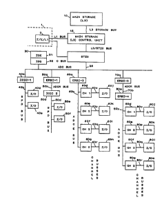
Fig. 1 shows a system diagram of a data processing
system incorporating the communication data bus of this
invention. A central processing unit 1 comprises an
instruction processing unit 2 which is connected to a
main storage unit 10 through main storage control unit
15 and to a storage input/output control unit (STIO)
20. Instruction processing unit 2 includes an
instruction unit, an execution unit, and an Ll cache
unit. In the preferred embodiment, the instruction
processor handles all IBM System 370 instructions. The
main storage (L3) control unit 15 provides a path to
main storage 10 for the storage operations of
instruction processor 2 and for input/output operations
involving main storage. The storage to input/output
unit 20 provides a path to main storage 10 for I/O
operations. The address/data/communications bus (ADC)
25 connects STIO 20 to input/output processor 30 which
includes an input/output engine (IOE) 31 and an
input/output gueue unit (IOQ) 32.
In the preferred embodiment the input/output
processor handles all IBM system 370 input/output
instructions.
The ADC bus 25 also serves to connect STIO unit 20
and IOQ 32 to the input/output interface controller
(IOIC-l) 40a, and extended remote bus interface unit
(ERBI-l) 50a, extended remote bus interface unit (ERBI-
2) 50b, and extended remote bus interface unit (ERBI-3)
50c. IOIC-1 40a provides control of the SPD bus (SPD)
40b. The ERBI-l unit 50a and ERBI-3 unit 70a provide
the bus extension function of the ADC bus 25 in the
form of ADCR busses 50b and 70b. ER8I-4 unit 80a
provides the bus extension function of ADCR bus 70b in
the form of ADCE bus 80b. ERBI-2 unit 60a provides the
EN9880}4
` ``8 1 ~ 3 7
bus extension function of the ADC bus 25 in the form of
ADCE bus 6Ob.
IOIC-2 50c provides control of the SPD bus 50d.
IOIC-l 4Oa is connected to the subunit processorS 4Od
and 40e over the SPD bus 40b. Similarly, IOIC-2 is
connected to the subunit processors 50e and 50f over
the SPD bus 50d. The channel processor units 60d, 60e,
60f and 60g are connected in common to ERBI-2 over the
ADCE bus 60b and individually to the I/O subunit
processors 60j, 60k, 601 and 60m, respectively, over
the channel busses 600, 60p, 60q and 60r, respectivelY
In like fashion, ADCE bus 80b leading from ERBI-4
80a connects to channel processing units 80d, 80e, 80f
and 80g. The I/o subunit processors 80j, 80k, 801 and
80m are individually connected to the channel
processing units 80d, 80e, 80f and 80g, respectively,
over the channel busses 800, 80p, 80q and 80r,
respectively.
The instruction processing unit 2 executes IBM
ZO System 370 instructions which are taken from an L1
cache unit. The results of the instruction execution
are stored in the L3 main storage unit 10. If it is
necessary to transfer the results to one of the various
I/O subunits 40d, 40e, 50e, 50f, 60j, 60k, 60i, 60m
80j, 80k, 801 or 80m, the I/o processor unit 30 sends
commands to the selected one of I/O subunits 40d, for
example, which then initiate a main storage 10
operation. When the selected one of the I/o subunits
40d is finished with the use of main storage 10, the
I/O processor unit 30 sends an ending status to the
instruction processor 2 indicating that the operation
is complete.
The ADC bus 25 provides a path for the I/o
processor unit 30 to communicate with the I/O subsystem
and storage 10. It also provides a path for the
EN988014
9 1318~37
various of the I/O devices to get to main storage 10.
Because of technology constraints, it is common to
limit the number of drops on a given bus. In a typical
bus the maximum number of drops which can be handled is
eight. The number of allowable drops is increased by
adding extended remote bus interface units 50a, 60a,
70a and 80a. The ERBI-2 unit 60a and ERBI-4 unit 80a
provide the capability to attach a standard IBM System
370 channel bus with the use of the channel processors
60d-60g and 80d-80g.
The ADCR buses have extended driving capability to
allow the physical extension of the bus to a remote
unit. The ADC bus 25, the ADCE bus 60b and 80b, and
the ADCR bus 50b and 70b each use the same remote
signals and bus handshake and pass the same information
for each operation. This extends the uniformity of the
bus interface throughout the I/O subsystem.
A command and the associated data sent from a bus
unit on the ADCR bus 50b is stored in ERBI-1 50a, which
then passes the command and data on ADC bus 25.
Similarly, a command and data from a unit on ADCE bus
60b is stored in ERBI-2 and then passed over ADC bus
25. The other ERBI units 60a, 70a and 80a function in
similar fashion.
Arbitration of the ADC bus 25 is handled by IOQ
unit 32. The logical arrangement of the arbitration is
conventional although the timing is different from
similar prior art systems.
Physical routing of the ADCE bus and ADCR bus is
shown in Fig. 2. The ADCR bus is a part of the cables
extending between the processor 1 and the remote units.
The ADCE bus is mounted on board wires. Fig. 3 shows
how the ADCE bus is daisy chained though channel
processor units cards or IOA's. In this arrangement,
the logic card wiring can be used for the ADCE bus
-
. ~ .
EN988014
13i8Q37
for an IOA bus. An IOA bus is used to connect I/O
subunits to an IOP which is then attached to an SPD
bus. In the daisy chain arrangement, each channel
processor unit card propagates the ADCE bus, and an IOP
breaks the chain. IOAs propagate the IOA bus. This
provides the ability to attach channel processor units,
IOP units or IOA units in the same logic card slot.
Each unit connected to either the ADC bus or the
ADCE bus must develop signals to be received or placed
on the bi-directional Address/Data/COmmand bus and the
control bus. The lines of the Address/Data/Command bus
and the control bus extend and connect to all bus
units. Each unit develops signals for and responds to
signals from the arbitration unit. The units`develop
signals for transmission to the arbitration unit
indicating message request and storage request and
respond to the grant signal from the arbitration unit.
Fig. 16 shows the fashion in which the various
handshake signals are developed. The DATA VALID signal
i8 developed when the count is equal to the length.
The BUSY signal is developed when the count is one less
than the length. -
The Address/Data/Command bus is a 36 bit, tri-
state, bi-directional bus consisting of 4 bytes with
parity. The bus is used to transfer storage data,
message information and commands between the various
I/O subsystem bus units. The control bus is a 4 bit,
tri-state, bi-directional bus consisting of 3 control
bits and one parity bit. It is driven by the bus unit
t~hich last received a Bus Grant signal. Bit 0 is the
COMMAND VALID bit. This signal indicates a valid
command is on the Address/Data/Command bus. All bus
units must sample the Address/Data/Command bus during
this cycle and determine if the command is for them.
Bit 1 is the DATA VALID bit. This signal indicates
that there is valid data on the Address/Data/command
bus. Bit 2 is the BUS BUSY bit. This signal indicates
the AddressjData/Command bus is busy and serves to
stop arbitration on the Address/Data/Command bus. The
bus unit driving this signal drives it inactive one
cycle before the last tra~sfer of data on the
Address/Data/Command bus. This signal can be developed
from the leading edge of the clock pulse immediately
preceding the clock pulse which gates data onto the
bus. B~ driving the BUS BUSY signal inactive one cycle
prior to the data signal, the arbitration unit has
sufficient time to determine which of the contending
busses is to be selected for the next transfer. Bit 3
Z0 is the parity bit or the bits 0-2.
The Processor Bus Operation (PBO) Status signals
are driven by the bus unit that receives the PBO
command to indicate status during the PBO operation.
The IOQ waits up to 32 cycles after a PBO command is
sent out on the ADC bus for either bit to be driven
active. A given implementation could utilize any
appropriate value but the preferred embodiment utilizes
32 cycles to represent the worst case delay required to
send a PBO command to a bus unit attached to the ADCR
bus. If neither bit is driven active during this time
the bus unit is assumed to be unavailable. An "01~ bit
combination indicates that the bus unit is busy. A
"10" bit combination indicates that the bus unit
received the PBO command and data with no errors. An
;EN98801~
` 12 131~37
~ bit combination indicates that an error has
occurred during the PBO operation.
MESSAGE REQUESTS are signals generated to obtain
access to the bus for Message Acceptance operations and
PBO Return Data commands. There is a unique message
request signal for each bus unit.
STORAGE REQUESTS are signals generated to obtain
access to the bus for L3 main storage operations. As
in the case for MESSAGE REQUESTS, there is one unique
storage request signal for each bus unit.
GRANTS are signals generated in response to
MESSAGE REQUESTS and STORAGE REQUESTS. These signals
are used to grant access to the bus. There is a unique
signal for each bus unit. The bus unit having the
highest priority at the time of request, as determined
by the arbitration units and the arbitration algorithm,
will receive the grant. The GRANT signal is developed
by the arbitration unit.
MESSAGE STATUS signals are driven at the end of a
MESSAGE ACCEPTANCE OPERATION to indicate the status of
the operation. If the operation is successful, this
signal is held active for one cycle. If the operation
failed, this signal is held active for two cycles.
The three primary uses for the ADC bus, the ADCE
bus and the ADCR buses include: (1) Tran5fer of
Processor Bus Operation (PBO) information. (2)
Transfer of data to or from L3 main storage 10. (3)
Transfer of message- information to the IOQ Message
Buffer.
Bus operations consist of arbitration cycles,
COMMAND VALID cycles, DATA VALID cycles and STATUS
cycles. A bus operation is initiated by activating a
request signal. Upon receipt of corresponding grant
signal, the requesting bus unit activates the COMMAND
VALID control signal and gates 4 bytes of command
~EN988014
13 1~18~37
information onto the Address/Data/Command bus 25.
During this cycle, Byte 0 always contains the command.
The specific commands are set forth in the showing of
Fig. 4. The particular bus unit for which the command
sent during COMMAND VALID is determined by the content
of the bus unit select destination field and, if
necessary, the channel identifier field.
The format and content of the bus unit select
field and the channel identifier field are shown in
Fig. 5. The bus unit select destination field
identifies either the IOQ, STIO, or IOIC connected to
ADC bus 25 or an IOIC connected to ADCR bus 50b or 70b,
or it identifies and ADCE bus. For channel processor
units connected to an ADCE bus 60b or 80b, the bus unit
select destination field will be shared by all the
units on that bus. In such cases, the channel
identifier field is used to identify the particular
channel processor unit and process ID for which the
command is intended.
Processor Bus Operations always oriqinate from IOQ
32 and consist of two types, COPY operations and LOAD
operations. A LOAD operation sends data from IOQ 32 to
another bus unit. A COPY operation takes data from a
bus unit and returns it to IOQ 32. For each PBO
operation, the bus unit which receives the command
responds with status information by driving the PBO
STATUS signals. The length of time between receiving
the PBO command and ~riving the PBO STATUS signal is
variable, allowing PBOs to be sent not only to IOICs
connected to ADC bus 25, but also to channel processor
units connected to ADCE busses 60b and 80b, as well as
IOICs connected to ADCR busses 50b and 70b. The
driving of this status signal is overlapped with the
next succeeding operation on ADC bus 25.
EN988014
14 1318~337
The COPY PBOs require two bus operations. Durin~
the first operation, the IOQ 32 sends the PBO command
and then disconnects from the bus, thereby freeing it
for other operations. In the timing diagram of Fig.
8, this is illustrated by the command on the
Address/Data/command bus and the subsequent PBO Status
"O" signal, which causes disconnection. During the
second operation, the bus unit which received the COPY
PBO command returns the requested data.
The system timing for the LOAD PBO operation is
shown in Fig. 6. At the time of COMMAND VALID the PBO
command is shown in Fig. 7 is on the bus. The PBO
command is specified by the content of bits 0-7, making
up the first byte. Bits 8-10 specify the message
priority value. The message priority value (MPV) sent
dur~ng the PBO operation indicates whether the command
is an asynchronous or synchronous command. If
NPV='OXX', the command is synchronous. If MPV='lXX',
the command is asynchronous. Bits 11-15 contain the
SPD bus command. Bits 16-19 contain the channeI ID
field. Bits 20-23 contain the bus unit select
destination field. Bits 24-25 specify the SPD bus
priority and are more fully described in the referenced
co-pending application corresponding to IBM Docket
Number EN987-063. Bits 27-31 contain the SPD bus
destination field which identifies the particular unit
to which the operation is directed.
At DATA VALID time the Address/Data/Command bus
contains the PBO data. At PBO status time, the PBO
status line contain the status of the PBO operation.
The system timing for the COPY PBO operation is
shown in Fig. 8. At the COMMAND VALID time the
Address/Data/Command bus contains the PBO command and
the fields passed are the same as those passed for the
LOAD PBO. The IOQ disconnects from the bus after the
IEN988014
131~37
CO~ND VALID cycle and waits for the return data. The
PBO STATUS time specifies the time when the bus line
contains the status of the PBO operation. At the time
of the COMMAND VALID signal the Address/Data/Command
bus contains the return PBO command. The DATA VALID
signal indicates that the Address/Data/Command bus
contains the requested PBO data.
Storage Operations originate from one of the IOICs
or one of the channel processor units or from the IOQ.
There are three types of storage operations: Read,
Write or Test and Set. Read takes data from the L3
main storage unit 10 and returns it to the unit that
requested it. Write takes data from the unit on the
bus and places it in L3 main storage 10. Test and Set
operations conditionally write one ~yte to L3 main
storage 10 and then return the L3 main storage data to
the requesting unit on the ADC bus 25. These
operations are initiated by sending a command to the
STIO 20. If the command is a Write, data follows
immediately after the command. For each operation the
requesting bus unit disconnects from the bus after the
transfer and waits for status information. This frees
the bus for other operations while the L3 main storage
10 operation takes place. When the storage operation
is complete the STIO 20 returns status for that
operation. If the operation is a read, the STIO 20
returns data immediately after the status.
The timing diag~am for the Write operation is set
forth in Fig. 9, and the structure of the command is
shown in Fig. 10. During the period defined by the
COMMAND V~LID signal, byte 0 contains the storage
command, and bits 8-11 contain the STORAGE KEY, which
performs the usual IBM System/370 functions, more fully
described in the IBM System 370 Principles of Operation
manual. Bits 12-15 contain the channel ID. Bits 16-
~EN988014
~ 16
~3~3~
l9 contain the bus unit select of the source bus unit.Bits 24-29 contain the length of the storage operation
to designate the number of ~ytes to be transferred,
less one. Bits 30-31 contain the address limit check
fièld. The address limit check field (ALC) is
specified by microcode. A oO' bit combination
indicates no Address Limit Checking.
A '01' bit combination indicates Data Address > =
Limit Check.- A '10' bit combination indicates Data
Address < Limit Check. A 'll' bit combination is
simply undefined and not used in this embodiment.
At the occurrence of the first DATA VALID cycle,
the Address/Data/Command bus contains the data to be
transferred to storage. After the termination of this
cycle, the bus unit discon~ects from the bus and waits
for a status signal.
As shown in the last line of the timing diagram of
Fig. 9, the Address/Data/Command bus contains the
status command in byte 0 and the status field in byte
1. The status field is defined as follows:
Bit 0 - ACB Check
Bit 1 - Key Check
Bit 2 - Address Limit Check
Bit 3 - Storage Hardware Error at NI0 Clock Rate
Bit 4 - Uncorrectable Error
Bit 5 - Storage Hardware Error at LEP Clock Rate
Bit 6 - Physical Memory Boundary Exceeded
Bit 7 - Key Arra~ Hardware Error
This field is used by the microcode to determine
the severity of the storage error.
With reference to Fig. 11 which shows the timing
diagram for the command structure for the read from
storage operation, the COMMAND VALID information is the
same as that for the previously described Write
operation. The first DATA VALID cycle presents the 31
IEN988014
1318~
bit storage address on the Address/Data/Command bus.
In a fashion similar to that previously described,
after the address information is presented, the bus
disconnects and waits for status and data. At the
occurrence of the second DATA VALID cycle the
Address/Data/command bus contains the returned storage
data.
The timing for Test and Set Storage is shown in
Fig.12 The Address/Data/Command bus contains the same
command information as the previously described Write
operation. During the first DATA VALID cycle, the
Address/Data/command bus contains the 31 bit storage
address. During the second DATA VALID cycle, the
Address/Data/Command bus contains the data for the
conditional write to storage unit 10. As previous}y
described, the unit disconnects from the bus at the end
of the first DATA VALID cycle and waits for status and
data.
The Address/Data/Command bus contains the status
command in byte 0 and the status field in byte 1 during
the STATUS COMMAND VALID cycle. During the second DATA
VALID cycle, the Address/Data/Command bus contains the
returned storage date.
Message operations are described with reference to
Fig. 13, which shows the command structure, and with
reference to Fig. 14, which shows the-timing diagram
for the operations. Message operations originate from
one of the IOICs or one of the channel processing
units. These operations take data from the bus unit
and put it in a message buffer in the IOQ 32. When the
message operation is complete, the IOQ 32 returns
status for that operation by driving the MESSAGE STATUS
signal. If the operation is successful, the IOQ 32
holds the signal active for one cycle. If the
EN988014
18 ~318~37
operation ~ailed, the IOQ 32 holds the signal active
for two cycles.
The Address/Data/Command bus contains the message
command information. ~ith reference to Fig. 13, byte O
contains the message command. Bits 8-10 contain the
message priority value. The message priority value
(MPV) sent during the message operation determines into
which message buffer in the IOQ a unit message goes.
If MPV = 'OXX' messages go into message buffer zero.
If MPV = 'lXX' messages go into message buffer one.
Bits 16-19 contain the bus unit select of the source
bus unit. Bits 20-23 contain the bus unit select of
the destination bus unit. Bits 24-29 define the length
of the message operation, designated one less than the
number of bytes that are to be transferred. As shown
by the DATA VALID signal, the Address/Data/Command bus
contains the message data for four cycles. The MESSAGE
STATUS signal indicates the status of the operation as
previously described.
Fig. 15 shows the logic arrangement for ~he ERBI
units 50a, 60a, 70a and 80a. The ERBI units provide
the I/O Bus extension for the processors I/O sùbsystem.
The units provide two logical paths. The first path
lies between the ADC bus 25 and the ADCE bus 60b. This
path has but one set of latches and controls in each
direction and therefore generates minimum delay. As
shown in Fig. 1 the ADCE bus 60b is used to drive
channels which are re~sident in the same logic card cage
as that in which the ERBI unit resides. In the
preferred embodiment, the functions of the ERBI unit
are packaged in a single semiconductor chip.
The other logical path lies between the ADC bus ~5
and the ADCR bus 5Ob or 7Ob, shown in Fig. 1. This
path includes an ADC bus to ADCR bus array (AR ARRAY),
a ADCR bus to ADC bus array (RA ARRAY) and the other
~N988014
lg ~ 318~37
controls required for the extension. The AR ARRAY is
used to store the information from the ADC bus if it
arrives when the ADCR bus is busy. If the ADCR bus is
not busy when the first word of ADC bus information
arrives, the AR ARRAY is simply bypassed, and the
signal flows directly between the latches as shown.
The ADCR bus to ADC bus array, RA ARRAY, is used to
store the information taken from the ADCR bus. The
information on the ADCR bus arrives and is latched with
clocks that are not synchronous with the ERBI unit
clocks. Therefore, when the first word of information
is written into the RA ARRAY, a start signal goes
through the metastability logic to request access to
the ADC bus. When the grant to send information on the
ADC bus is received, the information is read out of the
AR ARRAY. It will be appreciated that the RA ARRAY
sharply reduces the amount of time required for the
ERBI unit to be connected to the ADC bus in order to
pass information from the ACCR bus to the ADC bus. -
The ERBI unit permits use of the same bus protocol
at the ADC-ERBI interface which is a multidrop
connection, the ADCE-ERBI interface which is daisy
chained and the ADCR-ERBI interface which is normally
a high speed cable.
EN988014