Note: Descriptions are shown in the official language in which they were submitted.
~L31~3~9
45~qR 00481A
RAD~O CO~ICAT~:O~ D~e~
CO~TRO~ D FRBQ~ ~Y ~ A~ O~E~ T~
This application is a ~ivision of Canadian
Application Serial No. 548, 441 filed October 2, 1987 .
The present invention i5 r~lated to digitally
controlled radio con~unication devis~s and, more
particul~rly, to n~icroproc~s~or cc~ntrlalled,
~requency-~ynthesized radio frequency trarlsmitters and
receivers ( som~time hereinai~ter re~erred to ~s
"digital" radic~s).
BA~G~aollND aF ~g ~ O~
It is generally desirabl~ in mode~ radio-
telephone com~unic~tion to maintain a relativ~ly high
aver~ge carrier ~nodulation ~@vel while not exceeding a
predet~ined maxi~um modulatic~n l~el. ~hen a
modulated c~rrier ~ignal is detected in a radic~
receiver, the output of the receiver detector follows
the deviation o~ the received modulated carxier. It is
desir~ble to lhodulate the carrier at as high a level as
possible (consistenl: with bandwidth li~itations impos~d
by law and by trans~aitter and receiYer design~ to
-- 1
,;
,~
45MR 00481A
~31~3~
increase the u~eful receiver output level, and thus
increase communicationS range and decrease degradation
of received signal quality due to noise, fading and
other factors.
Transmitted carrier modulation level is determined
by the amplitude of the intelligence (e.g., voice)
signal applied to the modulating circuits (typically,
the oscillator or frequency synthesizer in frequency
modlllation transmitters). Signal processing such as
amplitude compression, amplitude limitinq and the like
can be used to increase the average carrier modulation
level. Ideally, average carrier modulation level
during useful signal transmission should remain
relatively constant at or near the maximum permitted
modulation level despite changes in parameters that may
affect transmitter modulation level (a.g., carrier
frequency, modulating signal characteristics, rf power
output, etc.).
Variation in modulation level wi~h change in
carrier frequency has not been a major problem in past
frequency modulation transceivers because transceivers
have generally been incapable of operating outside a
relatively narrow operating bandwidth. Hence, mos~
existing FM digital frequency-synthesized transmitters
do not provide compensation o~ carrier modulation level
for changes in transmitter operating freguency.
A typical prior-art synthesized transceiver is
capable of operating anywhere within a 20 MHz range,
and has a maximum carrier deviation level wnich varies
between about 3 and 5 kHz as carrier frequency
--2--
45MR 00481A
1 31 g359
is changed. In such prior-art transceivers,
modulation Level (i.eO, the effective gain of the
modulating circuits) is set to a fixecl level such
that a pr determined maximum modulation deviation
level (e.g., 5 kHz for narrow-band FM) is never
exceeded. United States laws governing radio
communications do not require a minimum deviation
level, but do set a maximum permissible modulation
level (and associated envelope bandwidth) -- so
that adjustment of maximum modulation level is
sufficient to guarantee tha~ the transceiver
always operates wi~hin the modulation level limits
set by law no matter what the carrier frequency is
set to.
This solution unfortunately has the
severe disadvantage that the transceiver carrier
modulation level is at or near th~ maximum
permissible level only for a few of the many
frequencies at which the transceiver is capable of
operating, and is far less than this maximum level
at many (if not most) transceiver operating
frequencies. Communications range and signal
quality and intelligibility are degraded on many
transmitter operating frequencies as a result.
~efore discussing the background of the
invention further, and other features of the
present invention, reference may be had by way of
example to the accompanying drawings in which:
FIGURE 1 is a graphical illustration of
exemplary variations in modula~ion deviation level
with change in operating frequency for a
45MR 00481A
~31~
transmitter with no compensation, a transmitter
with a non-linear compensation circuit, and a
transmitter with programmable compensation in
accordance with the present invention;
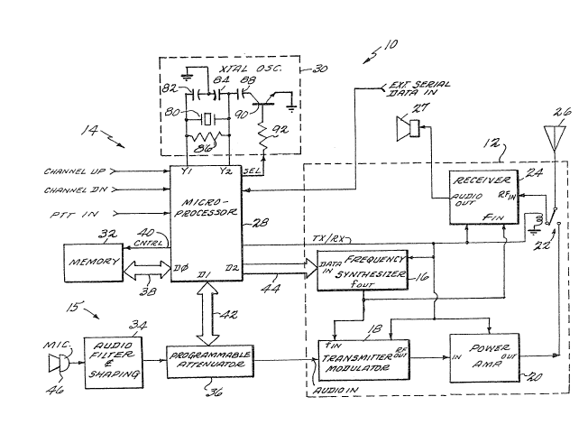
FIGURE 2 is a block diagram of a
presently preferred exemplary embodiment of a
microprocessor-controlled ra~io frequency
transceiver in accordance with the present
invention;
FIGURE 3 is a schematic diagram of an
exemplary circuit for use as the programmable
attenuator shown in Figure 2;
FIGURE 4 is a schematic diagram of the
data base stored in the memory shown in Figure 2;
FIGURE 5 is a schematic diagram of a
further circuit suitable for use as the crystal
oscillator shown in Figure 2; and
FIGURE 6 is a flowchart of somP of the
relevant control function steps performed by the
microprocessor shown in Figure 2.
Figure 1 i5 a graphical illustration of
carrier modulation deviation level of an exemplary
frequency-modulated radio transmitter plotted
against transmit frequency for various methods of
modulation deviation level compensa~ion. As the
curves marked "A" in Figure 1 show, variations in
modulation deviation level of an uncompensated
transmitter can be as much as 3 dB with a change
in operating frequency of 20 MHz. To add to this
problem, variations in modulation deviation level
between different production units may vary by as
45MR 00481A
much as 1 dB or more (as is depicted by three
different curves A-1, A-2 and A 3). Thus, the
modulation deviation of a completely uncompensated
transmitter might fall anywhera within the limits
between curves A-l and A-3. By a~justing the
deviation at center band (460 MHz in the example
shown) with a variable circuit component such as a
potentiometer, the total variation is limited to
that indicatad by curve A-2 (still 3 dB for a
change in operating frequency o~ + 10 MHz3.
Some countries of the world regulate
minimum as well as maximum FM deviation levels, so
that some correction of modulation level with
change in transmitter operating frequency is
lS necessary if legal requirements are to be complied
with. For example, some transceivers provide a
non-linear circuit within the transmittar
modulator which adjusts the audio modulation level
as a function of synthesizer tuning voltage. This
non-linear circuit provides some degree of
modulation level correction, ~ut the deviation
level is not programmable for individual operating
frequencies.
The curve of Figure 1 marked "B" shows
the variation in modulation deviation level for a
transmitter having additional non-linear circuit
components as described above. Such additional
compensation circuit components can reduce
variation in modulation level to less than plus or
30 minus O . 5 dB. Unfor~unately, unit-to-unit
variations in modulation deviation level requires
45MR 00481A
1318~9
overall modulator circui~ gain to he adjusted
(e.g., by adjusting a variable resistor
controlling the gain of one o~ the modulator
stages) so that the average modulation level is as
high as possible consistent with legal
requirements. Such adjustments are difficult and
time consuming to make, and must be individual
performed for each unit.
A technique which provides constant
transmitter modulation deviation level over a wide
range of transmit frequencies and which also
compensates for variations between transmitter
units would increase effective transmission range
and ensure complian~e with pertinent legal
requirements, and would therefore be highly
useful.
Another problem which often plagues
modern digital mobile radio transceivers is the
generation, by the internal circuitry of the
transceiver itself, of signals which interfere
with reception of desired signalsO Sophisticated
modern communications devices generally employ
high-spaed synchronous digital circuitry ~e.g.,
microprocessors) drivGn by clock synchronizing
25 signals. To obtain the speed per~ormance such
digital circuitry is capable of providing, it is
necessary to generate one or more clock
synchroniziny signals of relatively high frequency
(e.g., 4 MHz). Harmonics of the clock frequency
sometimes fall within the receiver operating
frequency band, causing spurious responses which
45MR 00481A
~183~
may interfere with the operation of the radio
transceiver.
For instance, suppose a radio
transceiver capable of operating in the 400 MHz
range with a receiver bandwidth of 12 kHz is
controlled by an internal microproce~sor driven by
a crystal o~cillator operating dt 4 MHz. If the
receiver of this transceiver is tuned to an
operating frequency of 464.000 MHz, a
clear-channel spectrum of 463.994 M~z to 464.006
MH~ much be maintained to avoid interference with
signals to be received. Unfortunately, an
on-channel spurious response may be caused by the
116th harmonic of the microprocessor oscillator
(4.o MHz x 116 = 46~.~00 MHz).
One solution to the problem described
above is to significantly improve the shielding
between the radio frequency circuitry and the
digital circuitry of the transceiver so that no
signals generated by the digital circuitry can
find their way in~o the RF circuitry. Because of
the high sensitivity and the compac~ness of modern
radio transceivers, it is extremely difficult to
provide sufficient shielding ~o guarantee complete
freedom from receiver interference.
Another method sometimes used to reduce
interference of received signals caused by
spurious signals generated by a microprocessor
clock oscillator is to select an oscillator
frequency which is not harmonically related to any
frequencies desired to be received. Although this
- 7
45MR 00481A
13~83~
solution works well for transceivers having only a
few fixed operating frequencies, modern
microprocessor-controlled radio transceivers are
capable of operating on a large number of channels
and can be programmed (or reprogrammed) in the
field to operate on new or different channels than
those selected at time of production~ It is
sometimes impossible to locate a clock oscillator
frequency which is not harmonically related to any
of a large number of possible operating
frequencies. Moreover, the clock oscillator
frequency may have to be changed every time the
transceiver is programmed to operate on new or
different operating frequencies, thereby
increasing field servicing time, cost and
complexity. An arrangement which guarantees
c o m p l e t e f r e e d o m f r o m i n t e r n a l
oscillator-generated receiver interference
regardless of receive frequency would be very
valuable and useful.
S~MM~RY OF ~ INVENTION
The present invention provides a method
and apparatus for controlling the frequency of
operation and at least one further variable
operating parameter of a radio transceiver.
A plurality of preset transmitter and/or
receiver operating frequencies are stored along
with corresponding information representing the
value of at least one further variable oparating
parameter of the radio transmitter and/or
receiver. One cf the stored plurality of
-- 8
45MR 00481A
~L 3 ~ 9
operating frequencies is selected, and the
operating frequencies o~ the transmitker and/or
receiver are set ~o ~he stored selected operating
frequency. The further variable operating
parameter of the ratio transceiver is controlled
in accordance with the stored further variable
operating parameter value corresponding to the
selected stored operating frequency.
For example, a plurality of preset
transmitter operating frequencies may be stored,
and, for each of the s~ored operating frequencies,
a corresponding preset modulation gain level may
also be stored. One of the stored plurality of
transmitter operating frequencies is selected and
a radio frequency signal at the selected
transmitter operating frequency is produced. An
input signal is amplified by an amplifier having a
gain set to the stored preset gain level
corresponding to the optimum gain valu~ for the
particular selected transmitter operating
frequency, and the radio frequency signal is
modulated with the resulting amplified input
signal.
A variable-gain amplifier may be used to
amplify the input signal. The gain of the
variable-gain amplifier may be set to the preset
modulator gain level correspondin~ to the selected
transmitter operating frequency. In one exemplary
arrangement, the gain-adjusted version of the
input signal is produced by an operational
amplifier output. The value of a resistance
45MR 00481A
~ 3 ~
connected hetween the operational amplifier input
and output terminals is adjusted to attain the
stored preset gain level associated in memory with
the selected transmit~er operating frequency.
The present inven~ion may thus
automatically compensate modulation deviation
level for changes in transmitte:r operating
frequency by permittiny a unique deviation level
to be programmed for each operating frequency (or
range of frequencies). That is, the output
amplitude produced by the transmitter modulator is
controlled by values stored in a memory associated
with data specifying transmitter operating
frequency also stored in memory. When a
transmitter operating frequency is selected, an
associated modulation level is thus also available
for automatic sPlection.
A different modulation level may thus be
programmed for each operating channel ~or subgroup
of channels), so that any operating
frequency-dependent non-linearities in the
transmitter modulator can be compensated for by
storing appropriate gain level information in the
memory circuit. Restated still differently, since
the modulation level o~ a ~requency-modulated
radio transmitter can be digitally programmed --
and since a desired specific modulation level is
specified for each radio frequency channel (or
subgroup), modulation amplitude can be programmed
to overcome modulator non-linearity and ensure a
substantially constant modulation level over a
-- 10 --
45MR 00481A
3 ~ ~
wide range of transmitter operating frequencies.
As another example radio receiver of the
type including a microprocessor may be controlled
to prevent spurious signals such as harmonics
generated along with a clock signal synchronizing
the operation of the microprocessor from
interfering with radio frequency signals desired
to be received.
Information representing a plurality of
preset receiver operating frequencies may be
stored, and, for each of the preset receiver
operating frequencies, corresponding control
information specifying one of at least a first and
a second state may also be stored. One of the
plurality of receiver operating frequencies is
selected, and a ratio frequency receiver is tuned
to receive the selected frequency in response to
the stored receive frequency information.
A microprocessor included in the
receiver device may be synchronized to operate at
a first frequency if the stored control
information corresponding to the selected receive
frequency specifies the first state, and may be
synchronized to operate at a second frequency
different from the first frequency if the stored
control information corresponding to the selected
receive frequency specifies the second state.
The synchronizing signal may be
continuously produced at a nominal frequency, and
may be shifted to a different frequency offset
from the nominal frequency whenever the stored
control information correspondiny to the selected
receive frequency specifies the second state. The
45MR 00481A
- ~3~
microprocessor clock frequency is thus either the
nominal frequency or the shifted frequency, a
selection be~ween the two being made as a function
receiver operating frequency.
A synchronizing signal of a nominal
frequency may be produced by a crystal oscillator
circuit as determined by the characteristics of a
crystal frequency- determining element. A
reactance may be switched into the crystal
oscillator circuit when the stored control
information corresponding to the selected receive
frequency specifies the second state.
Thus, the clock oscilla~or used to
synchronize the frequency of operation of the
microprocessor produces a frequency which is
selectively switched between two alternate
frequencies as needed to shift harmonics or other
spurious signals produced by ~he clock oscillator
out of the passband of the receiver. Such
frequency shifting is performed automatically as a
function of receiver operating frequency in
accordance with preprogramm~d information stored
in a memory along with the information which
determines receiver operating frequPncy.
DE~AI~ED D~SCRIP~ION OF PREF~RR~D ~M~ODIMENT
Figure 2 is a schematic block diagram of
a presently preferred exemplary em~odiment of a
frequency-modulated radio frequency transceiver 10
in accordance with the present invention.
Transceiver 10 includes a radio frequency (RF)
section 12, a digital control section 14, and an
audio input section 15.
- 12 -
45MR 00481A
~3~8~
RF section 12 includes a frequency synthesizer 16,
a transmitter modulator 18, a power amplifier 20, a
transmit/receive (T/R) switch 22 and a rec~iver 24. RF
section 12 ~perates in two alternate modes: a transmit
mode and a receive mode~ In the transmit mode, RF
section 1~ applies a modulated RF signal of a desired
frequency to an antenna 26. In the receive mode, RF
section 12 converts a modulated RF signal of a desired
frequency received by antenna 26 into a useful audio
signal. Details concerning the structure and operation
of RF section 12 will now be presented.
Frequency synthesizer 16 is a conventional
frequency synthesizer circuit which produces a
radio-frequency signal (at an output terminal fouT) the
frequency of which is controlled by digital data
applied to the DATA IN input of the circuit. Thus,
frequency synthesizer 16 may be considered a
digital-to-analog converter which converts digital
information inputted thereto into an analog radio
frequency signal (as understood by ~hose skilled in the
art, requency synthesizer 16 employs phase-locked loop
or similar arrangements to provide sufficient output
signal freguency stability at the frequencies at which
transceiver 10 operates).
The outpu~ fOUT of frequency synthesizer 16 is
applied to the input fIN of receiver 24. Receiver 24
in the preferred embodiment is a c~nventional
superheterodyne frequency-modulation receiver. The
input terminal RFin of receiver 24 is connected to
antenna 26 via T/R switch 22, and has an AUDIO OUT
- 45MR 00481A
~ 3 ~3~
output terminal which is connected to a loudspeaker 27
or other acoustic transducer.
P fOUT of frequency synthesizer 16
controls the operating frequency of the receiver 24
(e.g., the input terminal fIN of the receiver may be
connected to a conventional mixer circuit internal to
the receiver which produces a sum or difference
frequency resulting from heterodyning t:he fre~uency
synthesizer output signal and a signal of a desired
frequency received by antenna 26, the s~m or di~ference
frequency falling within the bandpass of a conventional
intermediate frequency (IE) circuit of the receiver, as
is well known). Receiver 24 may be entirely
conventional in design, and further details concerning
lS its function and operation may be found in a variety of
standard reference materials (e.g., The Radio Amateur's
Handbook published by the American Radio Relay League
(Newington, Connecticut> latest edition)).
The output fOUT of freguency synthesizer 16 is
also connected to an input fIN of a conventional
frequency-modulated transmitter modulator 18.
Transmitter modulator 18 may be a phase-shift FM
modulator of conventional design which
frequency-modulates (or phase-shift modulates) the RF
signal applied to its f~N input with an audio signal
applied to its AUDIO IN input, and produces a resulting
frequency-modulated RF signal at its RF OUT output
terminal (alter~atively, the voltage controlled
oscillator of freguency synthesizer 16 can be frequency
modulated by an audio signal). As will be understood,
-14-
45MR 00481A
~3~$3~9
the deviation (i.e., modulation index) of the modulated
RF signal produced by modulator 18 i5 determined by the
amplitude of the audio signal applied to the AUDI0 IN
terminal of the modulator.
The modulated RF signal produced by modulator 18
is applied to the lnput of a conventional power
amplifier 20. The output of power amplifier 20 is
connected to T/R switch 22 for application to antenna
26. Power amplifier 20 in the preferred embodiment may
be a conventional class C radio frequency amplifier
which amplifies the amplitude of the modulated RF
signal produced by modulator 18 to a desired level and
efficiently couples the amplified RF signal to antenna
26.
~ A transmit/receive (TX~RX) control signal applied
to RE section 12 controls whether transceiver 10 is
operating in the transmit or in the receive mode. This
TX/RX signal is applied to control inputs of modulator
18, power amplifier 20, receiver 24 and T/R switch 22.
Suppose, for example, that the TX/RX signal assumes a
logic level 1 signal level (high) when the transceiver
is in the transmit mode, and assumes a logic level 0
signal level (low) when the transceiver is in the
receive mode. When the TX/RX signal is at logic level
0, modulator 18 and power amplifier 20 are both
disabled, T/R switch 22 is controlled to connect
antenna ~6 to the input RFin of receiver 24, and
receiver 24 is enabled. In this receive mode, the
output of frequency synthesizer 16 controls the
frequency of signals received and demodulated by
receiver 24.
-15--
- 45MR 00481A
~3~8~
~ len the level of the TX/RX signal rises to logic
level 1, receiver 24 is disabled (and its AUDIO OUT
terminal is muted), transmitter modulator 18 and power
amplifier 20 are enabled, and T/R switch 22 is
controlled to connect antenna 26 to the output oX the
power amplifier. In the transmit mode of operation,
frequency synthesizer 16 produces an rf output signal
of a desired transmit frequency (or a subharmonic
thereof if power amplifier 20 includes conventional
frequency multiplying circuits) to be modulated by
modulator 18, amplified by power amplifier 20, and
applied via T/R switch 22 to antenna 26.
Digital control section 14 of transceiver 10
produces signals which control RF section 12 (e.g., the
TX/RX signal and the digital data which determines the
output freguency of the rf signal produced by frequency
synthesizer 16). In the preferred embodiment, control
section 14 includes a microprocessor 28 (or other
suitable digital signal processor), a clock oscillator
circuit 30, and a memory 32 (preferably a Random Access
Memory with a battery back-up to make it non-volatile
or an EPROM).
Microprocessor 28 in the preferred embodiment
includes three ~3) data input/output ports: DO, Dl and
D2 (although three separate I/O ports are shown, it
will be understood by those skilled in the art that
fewer I/O ports and I/O multiplexing could be used
instead). The DO I/O port of microprocessor 28 is
connected to the data input/output port of memory 32
via a plurality of bidirectional signal lines 38 (an
-16-
45MR 00481A
~31~ 3~
additional control signal 40 produced by microprocessor
28 controls the operating, e.g., read/write, mode of
memory 32). The D1 I/0 port of microprocessor 28 in
the preferred embodiment is connected to provide
digital information to programmable attenuator 36 via
data lines 42. The D2 I/0 port of microprocessor 28 is
connected, via data lines 44, to the DATA IN in~ut
terminal o fre~uency synthesizer 16.
Microprocessor 28 is connected to receive
additional control and/or data inputs from external
devices via additional signal lines (these additional
signal lines may be connected to spare inputs of I/0
ports D0-D2, or may be connected to an additional I/0
port (not shown) of microprocessor 28 if one is
available). A PTT IN signal input to microprocessor 28
is connected to an external transmit/receive controller
in the preferred embodiment (such as a push-to-talk
switch mounted on a microphone, the output of a
voice-operated relay (VOX), or the like). In the
preferred embodiment, transceiver lO operates in the
transmit mode when the level of the PTT IN signal is at
logic level 1, and otherwise operates in the receive
mode.
A signal CHANNEL UP and a further signal CH~NNEL
DN are applied to inputs of microprocessor 28 by ~n
external channel selector device (not shown) -- this
channel selector device could comprise, for example,
discrete channel up and channel down control switches,
a conventional channel selector switch and associated
encoder logic, or the like. Both the CHANNEL UP and
-17-
~ 45MR 00481A
~8~
CHANNEL DN signals are normally at logic level 0 in the
preferred ~mbodiment. When the CHAMNEL UP signal rises
to logic level 1, microprocessor 28 selects an
operating channel which is ~above~ (in frequency, in a
predetermined order, or both) the channel at which
transceiver 10 was operating previously. Similarly,
microprocessor 28 interprets a logic level 1 CHANNEL DN
signal as a re~uest to change the operating channel of
transceiver 10 to a channel which is "below" (in
frequency, in a predetermined order, or both) the
channel at which transceiver 10 was previously
operating on.
In the preferred embodiment, channels comprise a
transmit frequency and an associated receive frequency
pair, so that the signals CHANNEL UP and CHANNEL DN are
interpreted by transceiver 10 as requests to change
both the transmit and the receive frequency. For
example, a logic level 1 CHANNEL DN signal is
interpreted as a request to "decrement" the tra~sceiver
operating channel "number" to a different preset pair
of transmit and receive frequencies the user associates
with the decremented channel "number." It will be
understood that the transmit and receive frequencies
could be independently selected if desired.
The EXT SERIAL DATA IN line connected to an I/O
input of microprocessor 28 permits digital data
generated externally to transceiver 10 to be applied to
microprocessor 28. One use of the SERIAL DATA IN line
is to change the contents of memory 32. In this use, a
serial digital signal of a predetermined format
-18-
45MR 00481A
specifying new contents of memory 32 is pro~u~e~dr~9
externally to transceiver 10 (e.g., by a
mini-computer). This serial digital data is applied to
microprocessor 28 via the SERIAL DATA XN line,
Microprocessor 2~ in the preferred embodiment includes
an internal conventional UART (universal asynchronous
receiver/transmitter) which receives the data applied
to the SERIAL DATA IN line and converts this data to
parallel format. Microprocessor 28 then stores the
parallel-converted data in predetermined locations in
memory 32. In this way, the control functions of
microprocessor 28 can be programmed in the field.
A crystal oscillator 30 connected to
microprocessor 28 provides a clock synchronizing signal
for synchronizing microprocessor cycles, In the
preferred embodiment, crystal oscillator 30 produces a
clock signal at a frequency of apprsximately 4 MHz ~to
provide a microprocessor cycle time of 250
nanoseconds). A select output signal (SEL) genarated
by microprocessor 28 controls the frequency of crystal
oscillator 30 in a manner which will be explained in
further detail shortly.
The structure and operation of audio section 15
will now be descri~ed. Audio information to be
transmitted is produced in the preferred embodiment by
a conventional microphone 46 (although it will be
understood that any source of analog and/or digital
information may be used instead), The output of
microphone 46 is applied to the input of an audio
filtering and shaping circuit 34 (conventional in
-19-
45MR 00481A
1 3 ~
design) which processes the output of microphone 46 in
a conventional manner (e.g., by filtering it to remove
undesired frequency components, providing amplitude
limiting and/or compression to increase average
amplitude, reducing the amplitude of amplitude peaks,
and providing preamplification, all in a well-known
manner). The output of audio filtering and shaping
circuit 3~ is connected to the input of programmable
attenuator 36. The output of programmable attenuator
36 is connected to the AUDI0 IN terminal of transmitter
modulator 18.
Figure 3 is a schematic diagram of an exemplary
circuit or use as programmable attenuator 36 shown in
Figure 1. Programmable attenua~or 36 in the preferred
em~odiment includes an operational amplifier 50, a
four-to-one analog multiplexer 52~ a one-to-eight
analog multiplexer 54, a latch 55, a first plurality of
resistors 56a-56d, and a second plurality of resistors
58a-58h.
The analog audio output of audio filtering and
shaping circuit 34 (see Figure 2) is connected to the
inverting (-) input of operational amplifier 50
(through a series resistor 51 in the preferred
embodiment), and is also connected to a node 60
(through the series resistor). Resistors 56a-56d
(which together comprise a "ladder"-type resistor
network~ connect node 60 to different ones of anaiog
inputs of multiplexer 52. The analog common terminal
of multiplexer 52 is cor~ected to the analog common
terminal of multiplexer 54. The eight terminals of
-20-
45MR 00481A
~3183~9
multiplexer 54 ~the selected one of which depends upon
the digital value applied to the multiplexer select
inputs) are connected to a common node 62 through
different ones o~ resistors 58a-58h (which together
comprise a ladder-t~pe resistor ne~work). Node 62 is
connected to the output terminal of operational
amplifier 50.
The select inputs of multiplexer 52 and
multiplexer 54 are connected to signals produced by I/0
terminal D1 of microprocessor 28, and are applied to
the multiplexers via signal lines 42 (as will be
understood, these microprocessor-produced signals may
be latched and/or registered by latch 55 or a similar
device if desired).
In the preferred embodiment, a S-bit digital value
(word) controls the combination of resistors 56a-56d
and resistors 58a-58h selected by multiplexers 52 and
54. The two high-order bits of the 5-bit word control
which one of four terminals (00, 01, 10 or 11) is
selected by multiplexer 52, while the lower 3-bits of
the word control which of the eight terminals (000,
001, 010, 011, 100, 101~ 110 or 111) of multiplexer 54
is selected. For example, the five-bit digital word
10110 causes MUX 52 to select its "10" terminal and
controls MUX 54 to select its "110" terminalg thus
providing an analog signal path between the inverting
input and the output of operational amplifier S0
through series-connected resistors 56c and 58g.
The values of resistors 56a-56d and the values of
resistors 58a-5~h are chosen to provide desired signal
weighting over a desired range. As mentioned,
-21-
45MR 00481A
~31~3~
resistors 56a-56d and node 60 together comprise a
conventional resistor ladder network, as do r~sistors
58a-58h together with node 62. In one suitable
arrangement, the values of resistors 58a-58h may be set
as follows:
~58a = X, (la)
R b - X + ~X (lb)
R58c = X + 2oX, (lc)
R58h = X + 7~X ~ld)
(in the preferred embodiment, programmable attenuator
36 attenuates in linear steps, so that each step
increases by a constant resistance ~X3.
The values of resistors 56a-56d may be set in a similar
fashion, as follows:
~5~a = Y, (2a,
: R56b = Y ~ 8~X, (2b)
R56c = Y + 16~X, and (2c)
RS6d = Y + 24~X. ~2h)
The values X and Y are chosen in accordance wi~h the
open-loop gain of operational amplifier 50 and with the
values of other components associated with operational
-22-
45MR 00481A
~L31~3~
amplifier 50 (e.g., the value of resistor 51) to
produce desired range of gain of programmable
attenuator 36.
As shoul.d now be evident, programmable attenuator
36 functions as a closed-loop operational amplifier
with a fee~back resistance (i.e., the resistance
between output and input terminals) which is
programmable in response to a 5-bit digital word
applied to multiplexers 52 and 54 via signal lines 42.
The gain of programmable at~enuator 36 may be expressed
as follows:
GAIN = Rprog/R51
where Rprog is egual to the value of the one of
resistors 56a-56d selected by multiplexer 52 plus the
value of the one of resistors 58a-58h selected by
multiplexer 54 (ignoring effects of the BIAS signal
applied to the non-inverting input of operational
amplifier 50~. The gain of programmable attenuator 36
can be changed to any one of 32 different, discrete,
predetermined gain levels by applying the appropriate
5-bit digital value to the select inputs of
multiplexers 52, 54 via signal lines 42.
It will be understood that the circuit shown in
Figure 3 is only one of many different types of
digitally-programmed variable gain circuits which are
suitable for use in the preferred embodiment. Any
means or adjusting the gain of a linear amplifying
circuit in accordance with the value of a digital
-23-
45MR 00481A
13~8~
signal could be used instead of the programmable
attenuator arrangement shown in Figure 3 with good
results.
Figure 4 schematically shows an exemplary data
base 70 stored in memory 32 in the preferred embodiment
shown in Figure 2. Data base 70 includes a transmit
data base 72 and a receive data base 75 (receive data
base 75 will be described shortly). Transmit data base
72 includes a plurality of records 740~74n each
corresponding to a desired frequency channel on which
transceiver 10 is to transmit (for example, record 740
corresponds to a transmit channel TCM(0), record 741
corresponds to a transmit channel TCH(l), etc.).
Each of records 740 through 74 includes at least
two fields: a frequency field 76 and a deviation level
field 78. Frequency fields 76 contain digital words
which, when applied to the DATA IN input of fre~lency
synthesizer 16, cause the requency synthesizer to
produce a corresponding desired ret~uency at its output
fouT- Deviation level fields 78 in the preferred
embodiment contain a 5-bit digital word which, when
applied to programmable attenuator 36 via signal lines
42, cause the programmable attenuator to amplify the
audio signal applied thereto at a desired gain level.
2S The t~igital values stored in transmit data base 72
are obtained by first selecting the frequencies on
which transceiver 10 is to operate, and then
determining the digital values which must be applied to
fret~uency synthesizer 16 to obtain those operating
fretauencies (this conversion process is dependent upon
-2~-
45MR 00481A
~ 3~3~
the design of synthesizer 16, and is well-known to
those skilled in the art). Next, transceiver 10 is
controlled to transmit, in sequence, on each of those
desired frequencies, and the gain of programmable
attenuator 36 necessary to obtain (but not exceed) 100%
deviation o the FM RF signal applied to antenna 26 is
determined.
For example, suppose frequency fO (i.e., TCH(0))
is egual to 464.000 MHz. The digital word which, when
applied to the DATA IN input of frequency synthesizer
16, causes the frequency synthesizer to produce an
output signal of 464.000 MHz (or the appropriate
sub-harmonic of this frequency if freguency
multiplication is used) is stored in the field 76 of
record 740.
To obtain the value to be stored in field 78 o
record 740, the value of field 76 is applied to the
DATA IN input of frequency synthesizer 16, transceiver
10 is opérated in the transmit mode, a signal of the
maximum amplitude capable of being produced by
microphone 46 is applied to the input of audio
filtering and shaping circuit 34 (generally, microphone
46 should be disconnected for this operation and an
audio signal generator connected instead), and
different values are applied to signal lines 42 (to
thereby change the gain of programmable attenuator 36)
while the modulation level of the output of power
amplifier 20 is analyzed (using a modulation monitor, a
spectrum analyzer or in some other well-known manner).
45MR 00481A
The digital v~lue which, when ap~lied to
programmable attenuator 36, causes the output o power
amplifier 20 to have a modulation deviation level which
is the closest to (but not exceeding) 100% modulation
(i.e., which produces a deviation of 5 kHz for narrow
band FM) is stored in field 78 of record 740. This
process is repeated for each of the transmit
frequencies on which transceiver is to operate to
obtain n records 74, each including a frequency data
field 76 and an associated gain level field 78.
The above operation produces data which may be
inputted to a minicomputer via a user interface device
(e.g., a keyboard). The minicomputer is desirably
programmed to format the data into an appropriate
format, convert the data to a train of serial pulses,
and transmit the serial data to microprocessor 2~ via
the SERIAL DATA IN line (all in a well-known manner).
Microprocessor 28 con~erts the received data back to
parallel format and stores the data into memory 32 ln a
manner to be described shortly.
Once data base 70 is stored in memory 32,
microprocessor 28 selects one of records 740~74n in
accordance with signals applied to it via the CHANNEL
UP and CHANNEL DN signal lines. Microprocessor 28
preferably maintains an address pointer 77a ~e.g., an
internal register) which contains the address, in
memory 32, of the currently-~elected one of records
740~74n. The contents of this pointer 77a are
incremented whenever microprocessor receives a logic
level 1 CHANNEL UP signal, and are decremented whenever
-26-
45MR 00481A
1 3 ~
the microprocessor receives a logic level 1
CHANNEL DN signal (address "roll-over" may be provided
so that record 740 is regarded by microprocessor 28 as
having an address in memory 32 which is adjacent to the
address of record 74n~ as will be understood by those
skilled in the art).
Whenever transceiver 10 is operated in the
transmit mode, microprocessor 28 reads the contents of
frequency data field 76 of the addressed one of records
740~74n and applies the value read from this field to
the input of frequency synthesizer 16 to control the
transmit frequency of the transceiver -- at the same
time, the microprocess~r reads the contents of the gain
level field 78 of the addressed record 74 and applies
lS the 5-bit value it reads from thi.s field to the input
of programmable attenuator 36 to control the gain of
: the programmable attenuator. Thus, programmable
attenuator 36 is automatically programmed to amplify
the output of filtering and shaping circuit 34 at a
gain which is appropriate for the transmit frequency on
whi~h the transceiver is operating.
The cross-hatched band shown in Figure 1 labelled
"C" is a graphical representation of transmitter
modulation deviation level obtainable in accordance
with the programmable modulation compensation feature
of the present invention. Because the gain of
programmable attenuator 36 can be programmed for each
transmitter operating frequency, the variation in
deviatiQn may be maintained to within 0.15 dB of 100%
deviation using the 5-bit programmable attenuator 36 of
-27-
45MR 00481A
~3183~
the preferred embodiment (even less VariatiOIl is
possible if a programmable attenuator of higher
precision is used). Thus, modulation deviation level
is substantially constant over the sntire transmitter
operating range in accordance with the present
in~ention. No manual adjustment of any variable
circuit components within the radio transceiver is
required to obtain constant modulation deviation level
across the entire band.
Referring once again to Figure 2, the operation of
crystal oscillator 30 will now be described.
Microprocessor 28 operates with a cl~ck signal derived
from crystal oscillator 30, as mentioned previously.
Crystal oscillator 30 includes a crystal 80, capacitors
82 and 84, a resistor 86 and an amplifier circuit
contained within the microprocessor itself (many
conventional microprocessors contain such an internal
amplifier circuit).
Crystal 80 and resistor 86 are connected in
parallel across the Yl and Y2 terminals of
microprocessor 28, the Yl and Y2 terminals of the
microprocessor connecting to the microprocessor
internal oscillator amplifier. One terminal of
capacitor 82 is connected to terminal Yl, while the
other terminal of this capacitor is connected to ground
potential. Similarly, one terminal of capacitor 84 is
connected to terminai Y2, while the other terminal of
this capacitor is connected to ground.
-28-
45MR 00481A
13183~9
Crystal oscillator 30 in the preferred embodiment
also includes three additional components: a capacitor
88, an NPN transistor 90 and a resistor 92. One
terminal of capacitor 88 is connected to terminal Y2 of
microprocessor 28, and the other terminal of this
capacitor is connected to the collector of transistor
90. The emitter o transistor 90 is connected to
ground potential, while the base of the transistor is
connected to an SEL output of microprocessor 28 through
a series resistor 92.
m ose skilled in the art will recognize that
crystal 80, capacitors 82 and 84, and resistor 86
(together with the amplifier circuit internal to
microprocessor 28) generate an oscillator signal the
frequency of which is determined primarily by ~he
characteristics of crystal 80. However, when
transistor 90 is conducting, the oscillator frequency
is shifted slightly by the effect of the additional
capacitance added to the oscillator circuit by
capacitor 88.
When the SEL output of microprocessor 28 is at
logic level 0, no base current flows through the base
of transistor 90, and the transistor is in a
non-conducting state. Because transistor 90 has a
relatively high impedance when OFF, the transistor acts
as an open circuit in its OFF state and capacitor.88
has little or no effect upon the overall capacitance of
the circuit formed by capacitors 82 and 84, crystal 8Q
and resistor 86 -- in this state, oscillator 30 is
operating at its "normal" frequency (i.e., at or near
the resonant frequency of crystal 80).
-29-
45MR 00481A
~3~3~
When output SEL o microprocessor 28 rises to a
logic level l, base drive flows into transistor 90 to
turn the transistor ON (thereby completing the
connection between capacitor 88 and ground potential).
When transistor 90 is ON, capacitor 88 is connected to
the oscillator circuit to shift the resonant freguency
o crystal 80 slightly, and thus changes the frequency
of the clock signal generated by crystal oscillator 30.
Hence, when transistor 90 is conducting, crystal
oscillator 30 operates in a SHIFTED state ~i~e., the
signal frequency it produces is shifted somewhat from
the "normal" frequency of the oscillator).
Referring once again to Figure 4, it will be
recalled that data base 70 of the preferred embodiment
includes a receive data base 75. Receive data base 75
includes n records 940~94n' corresponding to receive
channels RCH (O) - RCH (n), respectively. Receive
records 940~94n each include a frequency data field 96
and a shift bit field 98. Frequency data fields 96
(which are analogous to frequency data fields 76 of
transmit record 940~94n) each contain a digital word
which, when applied to the DATA IN input of frequency
synthesizer 16, causes the frequency synthesizer to
produce a signal at its fOUT terminal having a
frequency which, when in turn applied to the fIN of
receiver 24, causes the receiver to receive on a
desired frequency.
The shift bit field 98 of each of records 940~94n
contains, in the preferred embodiment, a single bit
which has a nominal value of logic level 0, but which
-30-
45MR 00481A
~31~35~
may have a lo~ic level 1 value if necessary to prevent
a harmonic of the fundamental freguency clock signal
produced by crystal oscillator 30 from interfering with
signal reception, as will now be explained.
Suppose receiver 24 has a receive bandwidth of 12
k~7., crystal 80 has a frequency of 4.000 MHz, and it is
desired that receiver 24 be tuned to a receive
frequency of 464.000 MHz. Transceiver 10 can itself
produce no signal components within the range of
10 463.994 MHz and 464.006 MHz if interference with the
desired receive channel is to be avoided. However, an
on-channel spurious response might ~e caused by the
116th har~onic of the of crystal oscillator frequency
(4.00 MHz x 116 = 464.000 MHz).
To avoid interference, the frequency of
oscillation of crystal oscillator 30 can be shifted a
sufficient amount to move the 116th harmonic out of the
desired clear spectrum. The 116th harmonic should be
shifted in frequency at least 6 kHz, and, preferably 12
~ kHz (to provide a margin of error to allow for drifting
of the crystal frequency due to temperature or voltage
variations or due to aging).
If capacitor 88 shifts the frequency of crystal
oscillator 30 by 0.0025% (25 parts per million) when it
is connected in circuit (by the conductance of
transistor 90), the 116th harmonic of the crystal
oscillator is shifted an amount sufficient to eliminate
on-channel spurious response. The value of capacitor
88 should be relatively smal~ (i.e., approximately 20
picofarads) to cause this relatively slight shift in
-31-
45M~ 00481A
13~83~9
the fre~uency of oscillator 30 when transistor 90 is
turned ON without causiny runaway o crystal oscillator
30. It will be understood that the fre~uency of
oscillation of crystal oscillator 30 is lowered, not
raised, by the connection of capacitor 88 into the
circuit because of the electrical characteristics of
crystal 80.
Microprocessor 28 in the preferred embodiment
includes an additional address pointer 77b which is
used to address (i.e., point to) a selected one of
records 940~94n of receive data base 75. In a manner
analoyous to that described with respect to transmit
data base 72, logic level 1 C~ANNEL UP and CHANNEL DN
signals cause microprocessor 28 to select a different
one of records 940~94n than the one previously selected
by changing the value stored in register 77b.
When transceiver 10 is operated in the receive
mode, microprocessor 28 reads the contents of the
frequency data field 96 of the one of records 943-94~
addressed by its internal addressing register 77b, and
loads this information into freguency synthesizer 16.
The output of frequency synthesizer 16 in turn controls
the frequency at which receiver 24 operates. At the
same time, microprocessor 28 reads the contents of the
shift bit field 98 of the addressed one of records
9*0~94n' and applies this read one-bit value to its SEL
output for application to the base of transistor 90.
If the shift bit field associated with a stored receive
freguency contains a logic level 0, cry~tal oscillator
30 operates at its "normal" frequency. On the other
-3~
45MR 00481A
13~3~9
hand~ the frequency of operation of crystal oscillator
30 is shifted a predetermined amount if the contents of
the shift bit field 98 of the addressed one of records
940~94n is a logic level 1.
One suitable way of obtaining the values of shift
bit fields 98 is to first select the desired receive
freguencies of transceiver 10, and then operate the
transceiver at those desired frequencies, one at at
time. The shift bit field 98 is set for any o records
940~94n for which a spurious response attributable to a
harmonic generated by crystal oscillator 30 is
received. The values for shift ~it fields 98 of
different transceiver units can be made the same if the
transceivers are programmed to have the same receive
frequencies and also have crystals 80 with nearly the
same characteristics.
The amount by which the frequency of crystal
oscillator 30 must be shifted in order to eliminate
spurious on-channel interference is determined by the
RF channel bandwidth, the RF operating frequency, and
the tolerance of the crystal 80 (or other oscillator
frequency determining element). Sometimes, especially
in transceivers operating in the lower frequency bands,
it may be necessary to move the frequency of the
crystal oscillator 30 by several hundred parts per
million or more -- this frequency shift is greater than
can be accomplished by switching components other than
the crystal 80 itself.
Figure 5 is a schematic diagram of a further
exemplary circuit suitabla for use as crystal
oscillator 30 of the embodiment shown in Figure 2. The
-33-
45MR 00481A
~3~8~9
oscillator shown in Figure 5 includes two separatP
crystal oscillators llOa and llOb each of a
construction similar to that shown in crystal
oscillator 30 of Figure 1 (although, in the oscillators
shown in Figure 5, the amplifier internal to
microprocessor 28 is replaced by NAND gates 112a and
112b functioning as amplifiers in a well-known manner).
The SEL output of microprocessor 28 is connected
to an input of NAND gate 112a and is also connected to
the input of an inverter 114 (a NAND gate connected as
an inverter in the preferred embodiment) the output of
which is connected to an input of NAND gate 112b. The
outputs of oscillators llOa and llOb are connected to
respective inputs of a NAND gate 116. When the SEL
output of microprocessor 28 is at logic level 1, NAND
gate 112a becomes an inverting amplifier and oscillator
llOa is thus activated (at the same time, NAND gate
112b is disabled). If the SEL output of microprocessor
28 is at logic level 0, a logic level 1 is applied to
NAND gate 112b to cause it to act as an inverting
amplifier, thereby enabling oscillator llOb (and
disabling oscillator llOa). In this way, oscillators
llOa and llOb are alternately enabl~d depending upon
the level of the SEL output of microprocessor 28.
The resonant frequencies of crystals 80a and 80b
are offset by a desired amount ~e.g., 300 or 400 parts
per million) to provide a desired fre~uency shift in
response to a change in the level of the SEL output of
microprocessor 28. Thus, the arrangements described
can be used to cause a crystal oscillator harmonic to
-34-
` 45MR 00481A
13183~
be shifted off-channel even for transceivers operating
with relatively large bandwidth at low operating
frequencies.
There may be means known to those skilled in the
art for selecting and disabling oscillator circuits and
for controllably shifting the frequency of an
oscillator circuit. For example, in some applications,
the high stability provided by a crysta:L oscillator may
not be necessary or desirable, and the microprocessor
clock oscillator could in such cases take the form o a
voltage-controlled oscillator (VCO) the control voltage
of which is derived from a multi-bit shift field 98.
Other alternate, equivalent arrangements are possible
as is understood by those skilled in the art.
Figure 6 is an exemplary flow chart showing a
segment of the controlling programs including the novel
steps performed by microprocessor 28 of the preferred
embodiment under the control of software stored in
memory 32 (or in a read only program stored internally
to the microprocessor). In the flow chart shown in
Figure 6, control flow is rom top to bottom beginning
at the start block 150.
Upon startup, microprocessor 28 first determines
whether any externally-applied serial data is present
(block 152) by testing the contents of its internal
UART buffer (not shown) operatively coupled to the
SERIAL DATA IN line described previously. If serial
data is present, a byte of data is read from the SERIAL
DATA IN line (block 154) for s~orage into memory 32.
Memory 32 is enabled (block 156) (by applying an
-35-
45MR 00481A
~3~3~
appropriate control signal to it via signal line 40),
the data receiv~d from the SERIAL DATA IN line is
stored into the memory at a desired location (which may
be specified either by the serial daka itaelf or by tha
microprocessor progra~ming) (blocl~ 158)~ and the ~emory
is disabled (block 160). Control then returns once
again to decision block 152 to determine if additional
data is to ~e read from the SERIAL DATA IN line and
stored into memory 32. Blocks l5Z-160 are used to
program data base 70 a~ time of product:ion or in the
field, as described previously.
If no serial data is present on the SERIAL DATA IN
line (decision block lS2), microprocessor 28 determines
if a logic level 1 CHANNEL UP signal is present
(decision block 162). If the CHANNEL UP signal is
active, microprocessor 28 increments the contents of
the address registers (77a, 77b) pointing to records in
transmit data base 72 and/or receive data base 75
(block 164) (in some applications, where it is
desirable to select receive and transmit frequencies
independently, an additional control signal applied to
microprocessor 28 may be used ~o indicate whether the
channel to be incremented is the transmit channel or
the receive channel -- in other applications, such as
2S where repeaters having fixed pairs of input and output
frequencies are to be communicated with, pointers into
transmit data base 72 and receive data base 7S are
incremented and decremented simultaneously to preserve
desired pairing of receive and transmit frequencies).
-36-
45MR 00481A
i31~9
If microprocessor 28 determines that the C~ANNEL
UP signal ls not at logic level 1, but determines that
the CaANNEL DN ~ignal is active (i.e., is at logic
level 1) (decision block 165), microprocessor 28
decrements the contents of the address registers 77a,
77b pointing into transmit data base 72 and/or receive
data base 75 (block 166). In either case,
microprocessor 28 enables RAM 32 (by applying an
appropriate control signals to it via control lines 40
(block 168), reads data from the one of records 740~74n
and the one of records 940~94n pointed to by the
receive and transmit address registers (block 170), and
subseguently disables memory 32 (bl~ck 172). After
memory 32 is disabled, control is returned to decision
block 162 to determine whether additional channel
changes are desired.
If both the CHANNEL UP and the C~ANNEL DN signals
are inactive (decision blocks 162, 165), microprocessor
28 determines whether the PTT IN signal is active
(decision block 174) -- if it is, transceiver 10 is to
operate in the transmit mode. To transmit,
microprocessor 28 loads the contents of frequency data
field 76 read from the one of transmit records 740~74n
pointed to by the transmit address register 77a (and
read by block 170), and loads this frequency data into
frequency synthesizer 16 (block 176). Microprocessor
28 then loads the value read by block 170 from the
deviation gain le~el field 78 corresponding to the
selected freguency data field 76, and applies this gain
level data to programmable attenuator 36 via signal
-37-
45MR 00481A
~3~3~
lines 42 (block 178). Finally, microprocessor 28
enables modulator 18 and power amplifier 20 (and
disables receiver 24) by causing the TX/RX signal line
to rise to log}c level 1 (block 180).
Control then returns to decision b:Lock 174 to
determine if the PTT IN signal is still at logic level
1 -- if it is, blocks 176--180 are performed again and
transceiver 10 continues to transmit. If, on the other
hand, the signal PTT IN has fallen to logic level 0,
microprocessor 28 disables transmission by causing the
TX/RX signal to fall to logic level O (thereby
disabling modulator 18 and power amplifier 20 and
enabling receiver 24) ~block 182). The contents of the
frequency data field 96 of the one of records 940~94n
1~ read by block 170 are then loaded into frequency
synthesizer 16 to cause ~he receiver 24 to operate on
the desired receive frequency (block 184). As will be
understood, blocks 176-180 (and blocks 182-188) need
only be performed once (when the PTT IN signal first
changes state).
If the shit bit field 98 of the selected one of
records 940~94n read by block 170 is set (decision
block 186), the microprocessor 28 applies a logic level
1 to its SEL output to shift the frequency of crystal
oscillator 30 (block 188). Otherwise, microprocessor
28 applies a logic level O to the SEL output to cause
the crystal oscillator 30 to operate at its "normal"
frequency. Control then returns to decision block 152
to test once again for the various inputs as described.
While the present invention has been described
with what is presently considered to be the most
practical and preferred embodiments, it is to be
-38-
45MR 00481A
~ 3183~
understood that the appended claims are not to be
limited tc> the disclosed embodiments but on the
contrary, are intended to cover all modifications,
variations and/or ec~ivalent arrangements which retain
S any of the novel features and advantages of this
invention. By way of non--limiting example, although
the preferrecl embodiment of the present: invention is a
radio transceiver, the invention could be used with a
transmitter, a receiver, or other radio communications
device.
-39-