Note: Descriptions are shown in the official language in which they were submitted.
13183~
NE-198
TL~i OF THE INVENTION
2 "Dual-Mode Teleconferencing System"
3 BACKGROUND O~ THE INVEMTION
4 The present invention relates 8;enerally to teleconferencing systems,
S and more particularly to a dual-mode telecon:~erencing system.
6 With conventional teleconferencing systems"~notion-picture signals7 can only be transmitted from a motion-picture vide:o encoder and received
8 only by a motion-picture video decoder. Likewise, still-picture signals can
9 only be t~ansmffled from a still-picture video encoder and received only by
a still-picture video decoder. The incompatibility betwen motion-picture
11 and still-picture transmissions arises from the differences in coding
12 techniques employed in the motion-picture and still-picture video
1 3 encoders.
14 SUMMARY OF THE INVEiNllON
It is there~ore an object of the present inverltion to provide a
16 teleconferencing sys~em which eliminates the incompatibility pr~blem by
17 allowing still-pic~re signals and motion-pichlre signals to be transmitted
18 either from still-picture and dual-mode video encoders and received by
19 dual-mode video decoders.
2 0 According to a first aspect of the present inYention, ~here is provided
21 a still-picture video encoder for a teleconferencing system. This encoder
2 2 comprises a frame memory and a control circuit that con~rols writ~in and
23 readout of the frame memory by writing video samples of a frame of a
2 4 motion-picture signal into the memory and reading stored video samples
2 s from the memory at frame in~ervals. An encoder circuit is providecl for
2 6 encoding video samples read out of a location of the frame memory which
131~3~1
NE-1 98
corresponds to at least one scanning line period of the frame into a signal
2 representative of an intraframe correlation between adjacent ones of the
3 video samples and generating a signal of a constant value during
4 remaining line periods of the frame. The location oÇ the frame memory
s from which video samples are read out is sucsessively shifted by at least
6 one scanning line at ~rame intervals until all the video samples are encoded
7 using the correlation between successive ~ides~ samples.
8 According to a second aspect of the present invention, a dual-mode
9 video eneoder is provided which comprises a frame memory, an encvder
10 circuit, and a control circuit. The control circuit vvrites video samples of a
11 frame of a motion-picture signal into the frame memory and reads the
12 stored video samples at frame intervals from the fraTne memory during a
1~ still-picture mode. During a motion-picture mode, the control circu*
14 supplies the motion-picture signal to the encoder circuit. During the still-
15 picture mode, video samples are read out of a location of the memory
16 corresponding to at least one scanning line period of the frame and
17 translated into a signal representative of an intraframe correlation
18 between adjacent video samples and a signal of a constant value is
19 generated for remaining line pe~iods of the frame. During the motion-
2 0 picture mode, the encoder circuit translates video samples of the motion-
21 picture signal for at least one scanning line period into a signal
2 2 representative of the intraframe correlation and translates video samples
2 3 of the motion-picture signal for remaining line per~ods of each successive
24 frame into a signal representative of an interframe correlation between
2 5 successive frames. The }ocation of the frame memory from which video
2 6 samples are read is successively shifted by at least one scanning line at
131~
NE-198
~rame intervals during the still-pictlLre mode, and the scarming line whose
2 video samples are encoded is successively shifted at fraIne intervals during
3 the motion-picture mode.
4 According to a third aspect of the invention, a dual-mode video
S decoder is provided for r~ceiving a data bit stream either from the still-
6 picture or dual mode video encoder. The data bit stream contains a first
7 code identifying a signal representative of an intraframe correlation
8 between successive video samples during either of motion-picture and
9 still-pic~ure modes and a second code identifying a signal represen~ative of
10 an interframe correlation bet~een successive frames during the motion-
11 picture mode or identifying a signal having a constant value during the
12 still-picture mode. A first delay loop is r~sponsive to a detection of the first
13 code for successively causing an adder to provide summatioII of sucæssive
14 ones of the intra~rame correlation representative signal. A second delay
15 loop is operable during the motion-picture mode for delaying an output
16 signal from the first delay loop and the interframe correlation
17 representative signal for a period of the frame and is responsive to a
1 8 detection of the second code for causing the adder to provide su~unation of
19 the delayed signals with the interframe correlation representative signal
2 0 of a subsequent arrival, and further delaying the last-mentioned summed
21 signals for a period of the frame to repeatedly cause the adder to provide
2 2 summation of the further delayed signals with the inter~rame correlation
2 3 representative signal of a later arrival. During the still-picture mode, the
2 4 second delay loop delays an outpu~ signal from the first delay loop and the
2 s constant value signal of first arrival received from the video encoder for a
2 6 period of the frame and is responsive to a detection of the second code for
l 7~1 83~1
NE-198
causing the adder to provide summation of the delayed signals w;th the
2 constant value signal of a subsequent arrival. The second delay loop
3 further delays the last-mentioned summed signalls for a period of the
4 frame to repeatedly cause the adder to provide su:mmation of the further
S delayed signals with the constant value signal of a ]later arrival.
6 BRI~iF DESCRIPI'IOl~ OF THE Dl~WINGS
7 The present invention will be described in further detail with ~ef-
8 erence to the accompanying drawings, in which:
9 Fig. 1 is a block diagram of a telecc>n~erencing system according to the
10 presen~ invention;
11 Fig. 2 is a block diagram of a first form of the dual-mode -video
12 encoder of the p~esent invention;
13 Figs. 3A and 3B are schematic illustrations useful for describing the
14 operations of the dual-mode video encoder of Fig. 2 during motion-picture
mode and still-picture mode, respectively;
16 Fi~. 4 ~s a drcuit diagram of the c~ntrol circuit of Fig. 2;
17 Fig. 5 is a timing diagram associated with t~e circuit of Fig. 4;
18 Fig. 6 is a block diagram of a first form of the dual-mode video
19 decoder of the preænt invention;
2 0 Fig. 7 is a schemtic illustration useful for de~cribing the operation of21 the dual-mode video decoder of Fig. 6;
2 2 Fig. 8 is a block diagram of a second form of the dual-mode video
2 3 encoder of the present invention;
24 Fig. 9 is a block diagram of a second fornn of the dual-mode video
2 5 decoder of the present invention;
26 Fig. 10 is a block diagram of a first form of the still-picture video
13~381
NE-198
encoder of the p~sent invention;
2 Fi~. 11 is a block diagram o~ a second fonn of the still-picture video
3 encoder of the present invention;
4 Fig. 12 is a block diagram of a third form of the still-p~ctur~ video
S encs:)der of the present invention, and
6 Fig. 13 is a block diagram of a third fs:~rm of the dual-mode video
7 encoder of the inYention.
8 DETAILED DESCRIPTION
9 Referring now to Fig. 1, there is shown a teleconferencing system
10 according to the present invention. The system comprises a plurality of
11 dual-mode (motion-picture and still-pichlre modes~ video encoders 200-1
12 to 200-m and a plurality of still-picture video encoders 30~1 to 30~n at the
13 transmit end of the system and a plurality of dual-mode video decoders
14 400-1 to 400-k at the receive endO The e:ncoders 200 and 300 are com~ected
15 to line ~erminals of a public or private telephone sw~tching system 500 and
16 the decoders 400 are connected to line terminals of a telephone switching
17 system 600. The outgoing t~unk terminals of the switching systen 500 are
18 connected by a plurality of high-speed communication channels and low-
19 speed communication channels to corr~sponding incoming t~ terminals
20 of the switching sys~em ~00. Dual-mode encoders ~00-1 to 200-m are
21 accessable through the high-speed communication channels to any of the
2 2 dual-mode video decoders 40~1 to 40~k du~ing a motion-picture mode or
2 3 by way of the low-speed communication channels to any of the dual-mode
24 video decoders during a still-picture mode. Still-picture video encoders
2 s 300-1 ~o 300-n are, on the other hand, accessable only thr~ugh the low-
2 6 speed communication channels to any of the dual-mode video decoders
1318381
NE-198
1 ~00.
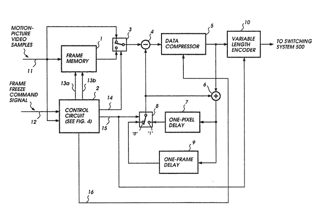
2 Referring to Fig. 2, each of the dual mode video encoclers 200 is
3 provided with a frame memory 1 to store a single frame of motion-picture
4 digital video samples supplied through an input line 11 in response to a
S write enable pulse supplied through line 13a from a control circuit 2 and
6 repeatedly read out the stored frame from the mernory 1 ~or transmission
7 of still-picture signals. During a still-picture mode, control circuit 2
8 receives a *eeze frame command signal, or logic-1 pulse throu~h an input
9 line 12 to operate a switch 3 through control line 14 so that it couples ~e
output of frame memory 1 to a subtractor 4. During motion-picture
11 modes, the control line 14 is at logic 0 and control circuit 2 operates the
12 switch 3 to connect the input line 11 to the subtractor 4. In either mode of
13 operation, the output of subtractor 4 is a differential signal rep~esentative
14 of a difference in digital value between an input video sample and a video
sample from a switch ~.
16 Switch 8 has a "1" pOSitiQn tersninal which is connected to the output
l 7 of a on~pixel delay circuit 7 and a "0" position te~inal which ;s connected
18 to the output of on~frame delay 9. In response to a logic-1 input on
19 contrs)l line 15 from control circuit 2, the output of switch 8 is connected to
2 0 the "1" position terminal and in response to a logic-0 input on line 15 it is
2 l switched to the "0" position terminal.
2 2 A data compressor 5 is connected to the output of subtractor 4 to
2 3 compress the quantization range of each differential video sample to the
2 4 range of values it assumes. If the original video sample is an 8-bit word,
2 5 the 256 quantum steps of the output of subtractor 4 are converted to 64
2 6 steps, for example, which can be represented lby a 6-bit word. With this
1318381
NE-l 98
data compression process, the amount of info~mation to be transmitted
2 can be reduced without affecting the quality of transmission. Data
3 compressor 5 is constructed of a read~nly men ory whieh stores ~bit data
4 words in locaffons addressable as a f~nction of 8-bit higher significant
address inputs supplied from the subtractor 4 in addition to a binary "0"
6 lower significant address input which is supplied throllgh control line 16
7 from the control circuit 2 when a scanning line is being "refreshed" in a
s manner as will be described d-mng either mode of operation. The ROM 5
9 also stores a binary "0" which is recalled as '~invalid" data instead of s~ored
data, regardless of the contents of the differentlal output signal from
11 subtractor 4, when the control line 16 is at logie 1. Control circuit 2
12 generates this logic 1 pulse when signals in the area of still-picture frame
13 other than the "refreshed" line is being read out of frame memoly 1.
14 The output of ~ata compressor 5 is supplied to one input of an adder
6, the output of which is coupled to the on~pixel delay 7 and on~frame
16 delay memory 9. On~-pixel delay circuit 7 delays its input by one pixel
17 period to detect differences between successive video samples at the output
18 of subtractor 4 utilizing the correlation between successive pixels
19 ~interpixel coding), and on~ame clelay memory 9 delays its input by one
2 O frame period to detect differences between pL~cels spaced one-frame period
21 apart utilizing the correlation between successive frames (interiFrame
2 2 coding).
2 3 Adder 6 takes its another input from the outputs of delays 7 and 9
24 when switch 8 is in the "1" position terminal so that the sum of a
differential sample from da~a compressor 5 and a on~pixel delayed
2 6 sample from delay 7 recovers an original video sample at the output of
1 31 8381
NE-198 8
adder 6 and is stored into the one-frame delay memory 9 when a scanning
2 line is being "refreshed" during either mode of operation. In addition, the
3 sum of a differential sample from compressor 5 and a one-fran e delayed
4 sample from delay memoIy 9 also results in the recovery of an original
S video sample at the output of adder 6 and is sto~ed again into the delay
6 memory 9 during non-refreshed periods of motion-picture mode.
7 However, during non-refreshed periods of still-piehlre mode, inval;d ("O")
8 bits are stored into the delay memory 9.
9 The output uf data cornpressor S is further applied to a variable
10 length encoder 10 which is responsive to a signal on control line 15 from
1 1 control circuit 2 to insert a code indicating whether the differential signal is
12 an interpixel coded signal or an interframe coded signal. Encoder 10
13 translates the differentially coded signals accor~ing to a high-efficiency
14 coding principle such as Huf~nan coding. The output signal f~m encoder
15 10 is applied to a co~responding line terminal of the switching system 500.
16 More specifically, during a motion-picture m{)de, control line 15 is
17 periodically switched to logic-1 level at frame intervals to connec~ the
18 switch 8 to the "1" position te~ninal so that, when video samples on the N-
19 th line of the N-th motion-picture frame (which is counted from a given
2 0 instant of time) are supplied through switch 3 to subtractor 4, the output of
2 l delay circuit 7 is applied to subtractor 4 as an interpixel (intraframe)
22 prediction signal as well as to adder 6. As a result, a series of ~bit
2 3 differentially coded video samples are derived by data compressor 5 from
24 successive video samples of the first line of the first of a series of M
2 5 motion-picture frames (where M represents the number of scanning lines)
2 6 and subsequently from successive video samples of the second line of the
1 3 1 838 1
NE-198
second frame, and so on. With the switch 8 being connected to the "1"
2 positîon ~erminal, video samples on the N th line of the N-th motion-
3 pichlre frame are dif~rentially coded and compress~d in data bit quantity.
4 This process is termed "refreshed" mode and a scaIming line being created
5 in this mode is called "refreshed". After being encoded vvlth Huffman
6 coding, the "re*eshed" line is transmitted to the motion-pictu~e decoder 20
7 and at the same time, original video samples recovered at the output of
adder 6 ~rom the "refreshed" line are stored into delay memory 9. Video
9 samples stored in the delay memo~ 9 in this manner are supplied during
10 the next frame period as an inte~frame prediction signal to subtra~or 4
1 1 when switch 8 is connected to the "û" position te~ninal in order to derive
12 differentially coded video samples from successive frames. With the switch
13 8 being switched -to the "0" position terminal during motion-pict~re mode,
14 the encoder performs interframe coding and original video samples
15 derived at the output of adder 6 during this mode are stored in~o the delay
l 6 memory 9. In this way, the scanning line which is refreshed is successively
17 scrolled to the next as video signals change from one frame to the next as
18 illustrated in Fig. 3a. During this motion-picture mode, control line 16 is
l g held at logic 0 level to allow data compressor 5 to perform data bit
2 o compression.
21 During a still-picture mode, the control circuit 2 applies a write
2 z er~ble pulse ~rough line 13a ~o frame memory 1 to store a single frame of
23 motion-picture signal and thereafter applies a read enable pulse at
2 4 periodic intervals to repeatedly read the stored frame as often as there are2 5 scan lines in the frame. Control line 15 is periodically switched to logic-12 6 level in response to the read timing of frame memory 1 so that, when video
1 31 8381
NE-198
- 10-
samples on the N-th line of the N-th readout are recalled from the frame
2 memory 1, the output of delay circuit 7 is suppli~ed to subtractor 4 as an
3 interpixel prediction signal as well il5 to adder 6. In this way, a series of
4 bit differerltially coded video samples can be deriv~ed by data compressor 5
from successive video samples of the Arst line of the stored frame during
6 the first reading of memory 1 and subsequently from video samples of the
7 second line of the stored frame during the second reading of memory 1,
8 and so on.
g During the still-picture mode, control line 16 switches to logic-û level
synchronously with the logic-1 timing of control line 15 in order to allow
1 1 data compressor 5 to perform data bit compression on differentially coded
12 samples of a scanning line to be refreshed, and switches to logic 1 during
l 3 the remainining line periods to cau~ the compressor 5 to generate a series
14 of "0" bits, or invalid data bits for non-~efreshed areas of the ~reeze frame
picture, which is indicated by dot~ed lines in Fig. 3b. In this way, the
16 re~reshed line scrolls line by line as in the case of motion-pic~re mode.
17 Variable length encoder 10 converts the output of compressor 5 into
18 Huffman codes in a manner similar to that of the motion-pichlre n~ode.
1 g 5ince the non-refreshed area of a fre~ze frame picture is converted into
~on bits, the total volume of still-picture information can be significantly
2 1 reduced.
2 2 Fig. 3 shows details of the eontrol circuit of Fig. ~. As shown, the23 control circuit 2 includes a type D flip-flop 200 having a D input port2 4 connected to the frame freeze comrnand input line 12. A sync separator 20
25 receives the motion-picture video samples through input line 11 to
26 separate vertical and horizontal sync pulses from the video components
1318381
NE-198 -11 -
and generates frame pulses (see Fig. 5~ as well as line pulses. The frame
2 pulse is applied to the clock input of flip-flop 20û so that the freeze
3 command signal is shaped into a pulse ha~ing exactly the duration of a4 frame period and appli~ as a write enable pulse through line 13a to the
S frame memory 1. The frame pulse is further applied to a frame counter 204
6 which is initialized by a reset circuit 2û5 which essentially comprises a
7 di~ferentiator and an inverter.
8 The reset pulse is further applied to $he set input oiF an RS fli~flop
9 207, the output of which is coupled to an AND gate 210 to cause it to pass
frame pulses through line 13b to frame men~ory 1 to sequentially read out
11 the contents of memory 1 at frame intervals. The output of fli~flop 207 is
12 further applied to control line 14 as a mode select signal indicating either
13 motion-picture or still-picture mode.
14 The output of frame counter 2û4 indicates the count of readouts of
frame memory 1 since the time of application of the frame freeze
16 command pulse to line 12. I~e output of ~rame counter 204 is applied to a
17 threshold de~ctor 206, which in tum supplies a reset puls to fli~flop 207
18 when the frame count reaches M~l. The line pulse from sync separator
19 201 is applied to a line counter 202 which is reset in response to each frame
2 o pulse to count seanning lines. The line count value and frame count value
21 aI~e supplied to a digital comparator 203. When th~ two count valuess are
Z 2 equal, comparator 203 supplies a logic-l output to an AND gate 20B as
2 3 well as to control line 15. There~ore, the output of AND gate 208 goes high2 4 at the N-th line of the N-th reading of memory 1.
2 5 The output of AND gate 208 is applied to an exclusive OR gate 209
26 to which the output of flip-flop 2û7 is also applied. Since the logic-l
.. 13l~38l
NE-198
- 12-
output of fli~flop 207 is of a duration equal to (M+1) times the frame
2 interval as seen from Fig. 5, the application of a logic-1 f~om ANr3 gate
3 208 to exclusive OR gate 209 causes its output to go low at times
4 synchronized with the read timing of each sucoessive line from memoIy 1.
S As shown in Fig. 6, dual-mode video decoder 400 comprises a
6 variable length decoder 30 which is connected to a corresponding line
7 terminal of the switching system 600. Signals received th~ough a low-
8 speed communication chamlel are decoded by a prncess inverse to that of
9 encoder 200 or 300 at the transmitter and the contents of the signals are
10 examined and a switching s;gnal is generated, indicating whether the
11 received signal is an interpixel differential signal or an invalid "0" bit
12 data. Decocler 400 applies decoded differential signals to a data expander
13 31 on the one lhand and the switching control signal to a sw*ch 32. Data
14 expander 31 performs expansion of the quantization range of the
15 differential signal to the original range by cs:mverting the ~bi~ word to an
16 ~bit word and supplies the converted word to one input of an adder 33
17 whose output is coupled to a one-pixel delay circuit 34 and a one-~rame
18 delay memory 35, and further through an output line 36 to a display
19 device, not shown, which includes a frame memory to reconstruct the
20 original ima~e. The output of delay circuit 34 is connected to the "1"
~1 position terminal of switch 32, the output of delay memory 35 being
2 2 connected to the "0" position terminal of switch 32. In response to a logic-
2 3 1 switching signal from decoder 30, the output of delay circuit 34 is applied
2 4 through switch 32 to the adder 33 and in response to a logic-0 output from
2 5 decoder 30, the output of delay memo~y 35 is coupled to the adder 33.
26 With a logic-1 switching signal being supplied from decoder 30,
1 31 83~1
NE-198
- 13-
differences between successive pL~els on each "re~reshed" line are supplied
2 to a~der 33 fr~m expander 31 and successively delayed and accumulated in
3 a feeclback loop formed by delay circuit 34, switch r32 ancl adder 33, so that
4 a replica of original video samples is recovered at the output of ~dder 33
5 and applied to the display device as well as to the dLelay memory 35. With
6 a logic-O input from decoder 30, invalid, "O" bit clata are supplied from
7 expander 31 to adder 33 and combined with data ~ad out of memory 35.
8 Therefore, at the end of reception of signals resulting from the fi~t
9 reading of frame memory 1 at the transmitter, signals recovered from the
10 first line of the freeze frame picture are stored into a first l;ne area of the
1 l delay memory 35 as indicated by a blank rectangle 40 in Fig. 7 and the
12 invalid data resulting from the second to the M-th line of the first reading
13 are stord in the rest of the emory ~5 as indicatd by dotted lines. In
14 response to the second reading of frame memory 1 at the transmi~er, the
15 first line of the recei~ed picture contains invalid "O" bit data and the
16 second line contains "refreshed" valid data, while the third to the M-th
17 line contain "O" bit invalid data. Therefore, the signals in the first line
1 8 area 40 of the memory 35 are summed with the invalid data of the first line
19 of the second read cycle and fed to the display as well as to the delay
20 memory 35. Valid signals on the second (refreshed) line of the second
21 readout are then sucoessively accumulated in the feedback loop of delay
22 circuit 34 and a replica of the original signals of that second line is
2 3 recovered and fed to the display as well as to the delay memory 35. The
24 invalid data on the third to the M-th line of the second readout are
2 s successively combined with invalid data read out of delay memory 35 and
2 6 applied to the display as well as memoly 35.
1 31 ~381
NE-1 98
- 14-
Therefore, at the end of reception of signals resulting from the
2 second readout, ori~inal signals of the first and second lines are
3 successively stvred in an area 41 of delay memo~y 35 as shown in Fig. 7.
4 When signals resulting fron the third readout are received, the
S signals stored in the area 41 are read out of delay mlemo:ry 35 and original
6 signals of the ffrst, second and third lines are recovered for delivery to the
7 display and for storage again into an area 42. As readout operations
8 proceed at the transmitter, recovered original signals of successive lines
9 are stored in an increasing area of delay memory 35 and applied
10 simultaneously to the display until the last line is reached, whereupon the
11 full storage area of delay memory 35 is filled with original signals as
12 shown at 43 in ~ig. 7. In this way, a still-picture image can be
13 reconstructed in the display as the re~reshed line scrolls down to the
14 bottom of a screen.
Referring to Pig. 8, a modlfied embodiment of the dual mode encoder
l 6 of Fig. 2 is illustrated. This encoder differs from the encoder of Fig. 2 in
17 that it includes an orthogonal encoder 50 and an orthogonal decoder 51
18 instead of the on~pixel delay circuit 7 of Fig. 2 and the "1" position
19 terminal of switch 8 is connected to ground. Orthogonal encoder 50 is
2 o connected to the output of subtractor 4 to perform orthogonal corlversion
21 on differential signals in spatial domain from subtractor 4 so that it is
2 2 represented by a corresponding value in frequency domain. The output of
2 3 orthogonal encoder 50 is applied to the data compressor 5 where the digit
2 4 is compressed and applied to the orthogonal decoder 51 as well as to the
2s variable length encoder 10. Orthogonal decoder 41 translates the
2 6 fr~quency domain signal to the original spatial domain signal and applies
1 31 8381
NE-198
- 15-
it to the adder 6 which, in turn, recovers original video samples by
2 summing the vutput of decoder 41 with a signal fr~m the switch 8.
3 During a refresh mode of either motion-picture or still-picture
4 transrnission, the "1" position te~ninal of switch 8 is connected to ground
s in response to a logic-l input on control line 15 to supply the ground
6 potential as invalid "0" bit data to the subtractor 4 The output of
7 subtractor 4 is a replica of its input signal f~om switch 3. The frequency
8 domain signal of this replica represents the differences between successive
9 pixels and is stored into the delay memory 9. When the control line 15 is at
10 logic 0, the output of one~frame delay memoxy 9 is connected to the
11 subtractor 4 to detect differences between successive frames. This
12 interframe difference signal is converted to a frequency domain signal by
1 3 encoder 50, compressed in clata bit by compressor 5 and converted back to a
14 spatial domain signal of iI~erframe difference by decoder 51 and summed
1 5 with the output of switch 8 by adder 6 to recover the original video sample
16 ~or storage in on~frame delay memo~ 9.
17 As shown in Fig. 9, anc~ther ~orm of the dual-mode video decoder 400
18 is shown which comprises a variable length decoder 60 and a data
1 9 expander 61 both being identical to t~ose shown at 30 and 31 in Fig. 6. The
2 o output of data expander 61 is coupled to one input of an adder 62 and an
21 orthogonal decoder 63. The output of adder 62 is coupled to the "0"
2 2 position terminal of a switch 64 and the output of orthogonal decoder 54 is
2 3 applied to the "1" position terminal of switch 64. Switch 64 is responsive to
2 4 the switching control signal f~om variable length decoder 60 to selectively
2 5 couple the signals applied to its terminals to a one-frame delay memoIy 65
2 6 as well as to an output line 6~. The output of delay memory 65 is connected
13183~1
NE-198
~,
to the other input of adder 62. Orthogonal decoder 63 performs
2 translation of a received fre~quency-domain signal to the original spatial-
3 domain signal of differential value to reproduce a replica of original video
4 samples, which is applied through switch 64 $o the output line 66 as well as
5 to the delay memory 65 when the interpixel differential signal is being
6 received. On receipt of invalid data bits, the switch 55 is connected to the
7 "0" position terrn;nal to apply the output of adder 62 to the delay memory
8 65, so that a sum of da$a read out of memory 65 and the received invalid
9 data bits are applied to the output line 66 and, at the same time, stored into10 memo~ 65.
11 Fig. 10 is an illustration of one for~n of the still-picture video
12 encoders 300. This video decoder is constructed from the video encoder of
13 Fig. 2 by removing from it the one-frame delay memory 9 and switches 3
14 a~ld 8 and directly conneeting the outputs of frame memory 1 and one-pixel
15 delay 7 to subtractor 4. With this configu~atlon, one-pixel delay 7 produces
16 differentially coded interpixel signals during the time the data compressor
17 5 is enabled in response to logic-0 input from line 16 and generates invalid
18 data during the time the data compressor 5 is disabled in response to logic-
19 1 inlput on line 16. The invalid data is combined with the input ~rom frame
2 0 memo~y 1 by the subtractor 4. I~e combined signal from the subtractor 4 is
2 1 disregarded by data compressor 5 as the latter supplies invalid, "0" bit data
2 2 to variable length encoder 10.
2 3 Another form of the still-picture video encoder is shown in Fig. 11 in
24 which the encoder is cons~cted from the video encoder of Fig. 8 by
25 removing from it the one-frame delay memory 9, switches 3 and 8,
2 6 subtractor 4, adder 6 and orthogonal decoder 51 and directly connecting
1318381
NE-l9~ - 17-
the output of frame memory 1 to orthogonal encoder 50. Orthogonal
2 encoder 50 constantly produces an interpixel correlated signal of ~bit
3 word, which is converted to a ~bit word signal when the data compressor4 5 is enabled in response to lo~ic-0 input from line 16 and is disregarded
S when data compressor 5 is disabled in response to logic-1 input from line
6 16 to produce invalid "0" bit data.
7 In Fig. 12, there is shown a fur~her embodiment of the still-picturevideo encoder. In this embodiment, iFrame memory 70 has a write emable
9 terminal (WE) connected to r~ceive a write enable pulse from control
1~ circuit 72 to freeze a frame of mohon-pieture video samples supplied on1 1 input line 71, and an address terminal (ADl~ through which it receives an
12 adc1ress signal to read out samples from each successive line specified by an
13 address signal from the control circuit 72 in the presence of a read enable
14 pulse supplied through its read enable terminal (RE) from the control
circuit 72. Control circuit n includes a line counter 721 which counts clock
l 6 pulses from a clock source 720 to generate a binary address signal at line
17 intervals as well as a carry pulse. Th~s address signal is applied to a lower-
18 significant input terminal of a read-only memory 723 and the carry pulse is
19 applied to a fFame coun~er 722. Frame counter 722 generates a bina~y
2 o address signal and a carry pulse at frame intervals. The binary address21 signal of the frame counter 722 is applied to a higher-significant address
2 2 input of the ROM 723 and the caITy pulæ of frame counter 722 is applied to
2 3 the clock input of a type D fli~flop 725 whose D input terminal receives
24 frame freeze command signal. A pulse having exactly the duration of a
2 S frame is generated by the fli~flop 725 and applied to the write enable
2 6 terminal of frame memory 70.
1 31 83~ 1
NE-198
- 18-
Read-only memory 723 has a plurality of memory planes. Each
2 memory plane is accessed by the frame address signal supplied to its
3 higher-significant address input from frame counter 722 and stores a series
4 of binary "1"s in locations which are successively accessed by the line
S acldress signal supplied to its lower-significant address input from line
6 counter 721. For example, the first memory plarle stores binary "1"s in
7 locatior~ which can be accessed when the line address input indicates the
8 first to the tenth line of the frame stored in memory 70, and the second
9 memory plane stores binary "1"s in locations which can be accessed when
10 the l;ne address input represents the eleventh to the twentieth line of the
1 l stored frame, and so on.
12 It can ~ seen that, by applying a series of binary "1"s from the ROM
1 3 723 as a read enable pulse and the line address input from line cour ter 721,
14 video samples can be read s:~ut o locations corresponding to the first to the
15 tenth line when frame address input of first occurrence is generated by
16 frame counter 722 following the writ~in operation of memory 70 and
l 7 subsequently video samples can be read out of locations corre~ponding to
1 B the eleventh to the twentieth line when frame address input of second
19 occurrenoe is generated by frame counter 722. Therefore, in a ~irst frame
20 interval, the initial ten lines (#1 to #10~ are sequentially read out of
2 l memory 70 and supplied to a subtractor 73 and in a second frame interval
2 2 the next ten lines (#11 to #2û) are sequentially supplied to the subtractor
2 3 73. The control signal for data compressor 74 and variable length encoder
24 76 is a logic-1 pulse which is derived from the output of ROM 723 by
2 5 appropriately delaying it by a delay circuit 726 so that the delayed binary
2 6 "1"s coincide with the timing of video samples. In response to a logic-1
1 31 8381
NE 198
pulse from control circuit 72, data compressor 7~ i~ enabled to perform
2 digit compression in a manner identical to that described in connection
3 with Fig. 2 and, in response to a logic^O input, it ceases digit compression
4 and generates invalid, "O" bit data. Variable length encoder 7~ perforrns
S high-efflciency coding in a manner idexltical to ~hat described in connection
6 with Fig. 2 and responds to the logic-1 input fr~m the control ci~cuit 72 by
7 inserting a code to the output data bit stream indicating that the signal
8 be2ng ænt is deri~7ed from inteIpDcel coding (refr~sh mode) and responds to
9 the logic-O inpu~ from the control circuit by inserting to it a code indicating
10 that the signal being sent is invalid data bits (non-refresh mode). In this
1 1 way, a plurality of successi~e scanning lines can be refreshed during each
12 frame interval.
l 3 A further embodiment of the present invention is shown ;n Fig. 13.
14 This embodiment differs from the Fig. 2 embodiment by the inclusion of
1~ two variable length encoders 10A and 10B which are coupled to the olltpUt
l 6 of data compressor 5. Each of these encoders is responsive to the signal
17 froIn control line 16 to insert signal idenffficaffon codes as in the preYious
18 embodiment, but operates in mutually exclusively times in response to the
19 mode select signal on control line 14. During motion-picture modes,
2 o control line 14 is at logic-O and encoder 10A is enabled in responæ thereto,21 and in still-picture modes control line 14 is at logic-1 and encoder lOB is
2 2 enabled. The outputs of encoders 10A and 10B are respectively cs:)nnected
23 through high- and low-speed communication channels 80 and 81 of a
24 switched network to dual-mode video decoders at separaté locations A
2s and B. This configuration permits a transmitter station to establ;sh
26 simultaneous video communication paths with two destinations. For
1 31 ~381
NE-198
- 20-
example~ if rnotion-picture signal is initially transmitted to the video
2 decoder at location A, and su~sequently swil:ehed to still-picture
3 transmission, the motion-picture frame of the last transmission can be
4 stored in the frame rnemory of the locatlon A for continued viewing and
5 the decoder at location B receives the still-pietu:re version of the last
6 transmission of the motion picture signals. In this way, the decoders at
7 both destinations can receive the same image simultaneously. Fu~ther
8 switching to motion-picture mode allows the location B to hold the still-
9 pic~re frame in its frame memory for continued viewing and the decoder
10 at location A to receive new motion-picture signals to update its ~rame
t 1 memory.
12 The foregoing description shows only preferred embodiments of the
13 present invention. Various modifications are apparent to tho~e skilled in
14 the art without departing from the scope of the present inveniion which is
1~ only limited by the appended claims. Therefore, the embodiments shown
16 and described are only illustrative, not restrictive.