Note: Descriptions are shown in the official language in which they were submitted.
` 1 31 8386
E~ECTROC~ROMIC, OXYGEN D2FICIENT
~E ~ LXTIC DEPOSITION
The present invention relatles to
electrochromic devlces which exhibit coloration and
bleaching thereof at ambient temperature by control
of the polarity of an indu¢ed electric field. More
particularly, this invention relatQR to
electrochromic devices wherein a layer of cathodic
electrochromic material comprising non-
stoichiometric, oxygen deficient metal oxide is
provided by pyrolytic deposition techniques~
Electrochromic devices are devices in which
a physical/che~ical change produced in response to
the induced electric field re~ults in a change in the
reflective (or transmissive properties) of the device
with respect to electromagnetic radiations, eOg., W,
IR, and visible radiation. Such devices, one
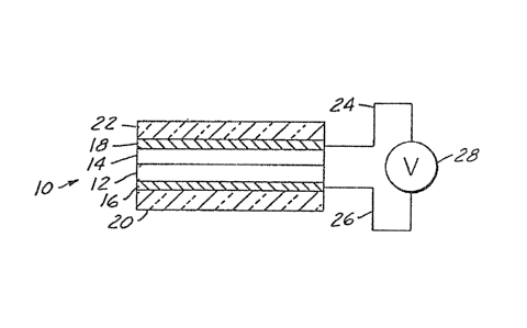
embodiment being shown as item 10 in Figure 1,
generally compri~e a film of electrochromic material
12 and an ion conductive insulating layer 14 which
functions as an electrolyte layer. rhe film and the
electrolyte layer are in surface contaot with each
2~ other ~or exchanqe vf ion~ between the el~ctrochromic
film and the electrolyte layer. Two conductive
electrode layers, 16 and 18 in Figure l, at least one
of them b~ing transparent, are disposed on the
opposite outer surfaces of the film and the
electrolyte layer to provide means for applying a
voltage across the combined thickness of the
electrochromic film and the electrolyte layer. The
electrode layer~, 16 and 18 in
. /
1 31 83~6
Figure 1, are provided on substrates, 20 and 22 of Figure
1, which substrates may be of a material such as glass.
The combination described is provided with external
electrical means for applying a voltage to the electrodes
to cause coloration of the electrochromic layer. By
reversing the polarity of the applied voltage, the
colored electrochromic layer will be uncolored
(bleached). Changing from the bleached state to the
colored state or f rom the colored state to the bleached
is termed ~'switching~. The electrochromic material may
be persistent in either its colored state or its
no~-colored state. By "persistent~ is meant the ability
; of the material to re~ain, after removal of the electric
field, in the absorptive state to which it is chanyed, as
distinguished from a substantially instantaneous
reversion to the initial state. The length of time a
material is persisten~ is called its ~memory".
Electrochromic devices o this type have been described
for several uses, such as image display, or light
20 filtering, etc.
In such devices~ the ~lectrochromic film usually
comprises an inorganic metal oxide material, m~st
commonly a transition metal oxide, in particular:
tungsten oxide. The el~ctrochromic metal 02ide layer has
been applied by a number of techniques: vacuum
deposition, chemical vapor deposition, thermal
evaporation, sputtering, and electron beam evaporation.
See, e.g., U.S. Patents ~os. 4,194,812; 4,278,329;
4,64~,308; 4,436,769; 4,500,878; 4,150,879; 4,652,090;
4,505,021; and 4,664,934. When tungsten 02ide is the
electrochromic material, the electrolyte layer is adapted
to provide a positively charged ion, preferably, a proton
or a lithium ion. The electrolyte layer is generally a
liquid electrolyte solution which comprises polymers or
131~338~
-- 3 --
copolymers containing acidic groups such as polystyrene
sulfonic acid or a compound like lithium chloride. The
electrolyte layer also may be a gel or a solid material.
One of the problems with the prior art devices
of this type is that the electrochromic layers of such
devices are not provided by methods which are suitable
for coating large areas such as would be necessary if,
e.g., su~roofs or windshields o automobiles were to be
made as electrochromic devices. As would be apparent~ it
would be advantageous to make such items electrochromic
devices which could be colored to a desired intensi.ty to
keep out radiation like W, IR and visible transmissions
; at will. For e~ample, it might be desirable to ~color~
the sunroof and the windows to allow minimum
transmittance when the automobile is parked to prevent
the interior of the automobile ~rom heating up on a sunny
day. In another embodiment, the windshield might be
colored to an intensity which allows operation of the
automobile yet reduces the amount of visible transmission
through the windshield.
Present methods for providing the electrochromic
layer also are generally incapable of providing an
electrochromic layer having sufficiently low transmission
o electromagnetic radiation. It is important to provide
a device capable of low transmission, particularly of IR
radiation, if the device is to be used as the sunroof or
windshield of an automobile. Another problem encountered
with prior art electrochromic devices is that they lose
their ability to switch with time, i.e., after numerous
switches the percent of electromagnetic radiation that is
transmitted by the electrochromic material in its colored
state increases. This is particularly problsmatic if the
device is to be used through many cycles to keep out
3 8 ~
undesirable radiation, as would be intended by a sunroof
or windshield of an automotive vehicle or windows o~ a
building. 5till another problem of such devices is that
the electrochromic material, i it is coupled with a
liquid electrolyte layer, has a tendency to be solvated
by the liguid electrolyte layer. This reduces the
durability of the device as well as the number of
switches through which it can suitably function.
An attempt to improve the resistance of
electrochromic materi.al to the degrading effects of the
electrolyte is taught is U.S. Patent 4,233,339 to
Leibowitz et al. It is disclosed therein that by
subjecting thin, electrochromic layers deposited on
substrate electrodes to a special heat treatment at a
selected high temperature for a selected short time, at
least a free portion o each layer is converted from the
amorphous to the crystalline form. It is further taught
that this outer layer of the electrochromic material
significantly increases the resistance of the
electrochromic layer to deyradation by the liquid
electrolyte. In U.S. Patent 4,175,837, to Yano et al, it
is disclosed that solvation of a tu~gsten oxide film can
be decreased by forming a WO3 film on a glass substrate
under conditions where the substrate is held at a high
temperature, that is, between 250C-450C. According to
that patent, the WO3 film is deposited by thermal
Pvaporation and vacuum deposition. It taught that tha
transparency of the WO3 film is undesirably lessened,
however, when the substrate is held above 450C during
the formation of the WO3 film.
It would be desirable if a method could be found
to form a durable electrochromic device capable of
substantially reducing transmission of electromagnetic
1 3 1 ~3~6
radiation, wherein the device is capable of switching Eor
prolonged periods of time without substantially any loss
of such electrochromic activity, and wherein the
electrochromic layer provided on a surface (i.e., on an
S electrode) would ~e resistant to dissolution by the
electrolyte. It would be most advantageous if a method
for providing such an electrochromic layer would be
simple and commercially suitable for coating large areas
- ea~ily.
The invention disclosed herein is capable of
overcoming the aforementioned problems o~ prior art
devices. The invention comprises providing the
electrochromic layer by pyrolytic deposition techniques.
Pyrolytic deposition techniques comprises
heating a surface and applying a composition at room
temperature onto the heated surface. For the sake of
convenience, the composition is generally sprayed onto
the heated surface. The heat from the hot sur~ace causes
chemical degradation of the sprayed composition and
subsequent recombination of components of the degraded
material with the ambient gas to form a material on the
surface. Various U.S. Patents describe the pyrolytic
deposition of metal oxides onto glass to change its
apparent color or reduce it transmission to
electromagnetic raaiation. See, e.g., U.S. Patents
4,217,392; 4,349,369; and 3,374,156. ~one of these
patents teaches or discloses an electrochromic device
wherein the electrochromic layer comprises oxygen
deficient metal oxide which has been deposited by
pyrolytic deposition as in the present invention.
`- 1 31 8386
In one a~pect, the pres~nt invention i8
directed to an electrochromic device comprising two
substrata~ and ther~between: one elec:trode layer, a
cathodic electrochromic layer, an ion conductive
layer and another electrode layer in that order,
wherein the cathodic electrochromic layer comprises a
non-~toichio~etric/ oxygen de~icient, variable
oxidation state metal oxide. The iorl conductive
layer comprises an ion source ms~n~ i~or providing ion
into the electrochromic layer upon application of a
voltage acros~ the electrode layers. The
electrochromic layer is deposited by pyrolytic
deposition onto a surface selected from a sur~ace of
the ion conductive ~aterial and a surface o~ the
electrode layer which surface i~ at a te~perature
between 500F and 1200F. Preferably, the
electrochromic layer is formed under the condition
where the surface is at a temperature between about
700F and 1100F, most preferably betwaen ~50F and
1100F. In this device, at lea~t one of the one
electrode layer and the other electroda layer is
transparent and each electrode layer is in contact
with one of the ~ubstrates.
Advant~geously, it has been ~ound that
preferred e~bodiments of the presPnt invention device
are capable of substantially preventing transmission
of all electromagnetic radiation. Additionally, in
another a~pect, a method of the present invention
appears to provide films of electrochromic material
which are more durable than those applied by
conventional depo~ition techniques. It ha~ been
found that embodiments of the present invention
device switched for a substantially long period o~
time and during this switching maintained their
a~ility to colour to the same intensity level while
switching. Additionally, embodiments of the
electrochromic layer of the present invention devicQ
~,~
1 3 1 83~6
have been ~hown to be re~istant to erosion
~dissolution) in the presence of the ion conductive
layar (electrolyte).
In the dascription which follows, rePerence
i~ made to the accompanying drawings, wherein:
Figure 1 disclose~ a schematic
repre~nkation of one embodiment of an elsctrochromic
device.
As discu~sed above, the electrochromic
device of the pr~s~nt invention comprises two
sub~trates and there~etween one electrode layer, a
cathodic electrochr~ic layer, an ion conductive
layer, and another electrode layer in that order. As
is known to those ~kill~d in th~ art, cathodic
electrochromic materials switch to the coloured state
when a voltage of negative polarity is applied to the
electrode adjacent the electrochromic layer. Devices
of thi~ general type are well known in the art and
disclosed for example in the U.S. Patents listed
above.
As disclosed above, we have found that by
providing a non-~toichiomstric, oxygen deficient
metal oxide (as a cathodi¢ electrochromic material)
by pyrolytic decomposition technique~, superior
electrochro~ic devices are obtain~d. Formation of
the cathodic electrochromic layer by this technique
as w@ll as each of the components o~ the
electrochromic device will be discus~ed in detail
hereinbelow.
Exemplary of non-stoichiometric, oxygen
deficient metal oxida~ u~eful as the cathodic
electrochromic material in this invention are those
selected from the group comprising tungsten oxide,
molybdenum oxide, vanadium oxide, titanium oxide and
copper oxide, wherein each of these oxides the oxygen
is less than stoichiometric.
~'
``-" 1 31 8386
Good cathod~c electrochro~ic materials
should be of the general for~la: MO~, where M is a
variable valence metal and x i~ a numbsr leBs than
that which will provid~ a ~toichiometric compound.
That is, for good cathodic electrochromic materials
the compound should be oxygen deficient, i.e., in a
reduced state. T~u~, as de~cribed in copending
Canadian patent application Serial No. 2,000,830-6
filQd Nove~bar 17, 1989, WO~, with x le~3 than 3 is a
good cathodic electrochromic mat~r$al wh~le W03 i8
not. (Presently ~03 iS understood to be electrochromic
but of less than de~irable electrochro~ic ~uality.)
Si~ilarly, VO~ with x less than 2.5 is a good cathodic
electrochromic material, while stoichiometric V205 is
not an electrochromic materia}. N~ither application
discloses forming the electrochromic layer by
pyrolytic decomposition techniques.
The metaI oxide, in order to possess the
de~ired electrochromic propertie-~, is required
according to this invention to be a
non-stoichiometric ~etal oxide which is oxygen
deficient. The degree to which the metal oxide is
non-stotchiometric is dependent on the particular
metal oxide e~ployed a~ the electrochromic material.
~5 Optimal non-~toichiometry for each metal o~ide useful
as the electrochromic material will be apparent to
one skilled in the art in view of the present
disclosure. Still other metal oxides, or compatible
mixtures of any of them, may be employed in the
invention. Selection of such other metal oxide will
be apparent to tho6Q skilled in the art in view of
the pre~ent discloeure.
1 31 ~3~6
g
According to this invention, the electrochromic
layer comprising a non~stoichiometric, o~ygen deficient
metal o~ide is deposited on a surface by pyrolytic
deposition under the condition where this surface is at a
temperature between about 500~F and about 1200F,
preferably between about 700F and about 1100F, most
preferably between about 850F and llCl0F. The surface
is selected from a surface of ~he elec:trode Iayer and a
surface of the ion conductive layer of the device. The
non-stoichiometric, osygen deficient metal o~ide can be
formed by pyrolytic deposition of a powder composition or
a liquid composition which comprises compounds containing
a metal having a variable o~idation state, which
compounds are capable of decomposing when subjected to
elevated temperatures and reacting with o~ygen to form a
non-stoichiometric metal oxide.
As di~closed above, the compositions employed in
the deposition of the electrochromic layer can be in
liquid or powder form. These compositions comprise
inorganic substances which contain at least one metal
element of a variable oxidation state, that is, at least
one element of the Periodic Table of Elements which can
e~ist in more than one o~idation state in addition to
zero. These include materials containing a transition
metal element (including Lanthanide and Actinide series
elements) and materials containing non-alkali metal
elements such as copper. Preferred materials of this
class are transition metal compounds in which the
transition metal may e~ist in any o~idation state from +~
to +80 Particularly useful metal compounds are those
which contain as the metal: tungsten, molybdenum,
vanadium, titanium, lead, bismuth, and copper. In the
case of a liquid, the liquid composition comprises a
dispersibl~ or dissolvable metal compound. Exemplary of
~ 31 8386
a liquid composition which can be em~loyed ~o
deposit, for example, a tungsten oxide ~ilm is one
comprising tungsten hexachloride dissolved in
~olvent~ ~uch a~ N,N-dimethylformamidle, hydrofluoric
acid and polar ~olvente includlng watler. A copper
oxide film can be depo~ited using a ~olution
compri~ing, e.g., aqueous copper nitr,ate. A nick~l
oxide film can be deposited, e.g., fro~ a solution
comprising nickel a¢etate in ethyl alcohol/liquid
am~onia. A molybdenum oxide film can be deposited,
e.g., a solution comprising cyclopentadienyl
~olybdenu~ tricarbonyl dimer in methylene chloride.
Exemplary of powder compo6ition~ which may
be employed according to th~ pre~ent invention to
pyrolytically deposit the electrochromic layer
include, for example, metal carbonyl~, metal
acetylaccetonates and titani~m isopropylate, with the
carbonyls being preferred. The co~position applied
by pyrolytic decomposition techniques according to
this invention can ~lso contain a mixture of
different metal compound~ wherei~ the metal or other
portion o~ the compound i8 different~ as would be
apparent to one skill~d in the art in view of the
pre~ent di~closure.
As ha6 been disclosed above, it is
critically important in this invention that the
cathodic electrochromic layer provided comprise a
transition metal oxide which is non-~toichiometric
and oxygen deficient. Deposition of a
non-stoichiometric metal oxide may be encouraged by
conditionc ~uch as: (1) including a reducing agent in
the powd~r~d co~position or liquid composition, (2)
providing a gas comprising inert gas or reducing gas
as a carrier gas for the powdered composition or
liquid composition, (3) providing, during the
pyrolytic deposition of the electrochromic layer, a
1 31 8386
11 --
gas comprising an inert gas or reducing gas near the
surface on which said eleGtrochromic layer is bein~
deposited, ~4j controlling the temperature of the surface
on which the electrochromic layer is being deposited and
~5) controlling the rate of deposition of the
composition, i,e., the amount of material/time being
atomized by the deposition equipment. These conditions
may be used, if desired, separately or in combination.
Still other ways in which deposition of a
non-stoichiometric metal oxide film may be provided will
be apparent to those skilled in the art in view of this
disclosure.
E~emplary oE reducing agents that could be
employed according to this invention include, for
example, phenyl hydrazine, formaldehyde, alcohols and
non-carbonaceous reducing agents such as hydroxylamine,
and hydrogen. Reducing elements such ~s Au, F, Pb, etc.
: may also be included in $he composition~ Such reducing
elements would codeposit with the electrochromic material
and be incorporated with the cathodic electrochromic
film. As disclosed above, another way to encourage
formation of a non-stoichiometric metal oxide film is to
provide a reducing environment by means of the carrier
gas or the gas near the surface on which the
electrochromic layer is being deposited. The carrier gas
employed according to this invention may, if it be
desired to provide a reducing environment in this way,
comprise a gas selected from any inert gas or reducing
gas, including, but not limited to gases such as
nitrogen, argon, carbon monoxide, carbon dioxide, and
hydrogen and gas mixtures including air ~ nitrogen, air +
nitrogen ~ argon, and the like. It is intended that,
while a carrier gas, e.g., comprising an inert gas such a
nitrogen, may be employed to provide a reducing
1 31 838h
12
environment, oxygen i5 still presQnt near the surface
on which the ~ilm is being depo~ited. ~h~ amount of
o~ygen near this ~ur~ace may be de¢recl~ed ~rom that
normally pre~ent, however, by ~mploying a carrier ga~
(comprising an inert or reducing ga~) or by providing
a gas near the sur~ace which will tend to di~place
BOme of thQ oxygen normally pr~nt near thi~
~ur~ace. Th~ optim~l amount o~ inert or reducing ga~
or reducing agent which could b~ employed according
to thi~ invention i~ that which would provide the
de ired non-~tolchiometric, oxygen de~icient
transition metal oxide according to thi~ invention.
Selection of optimal amount-R of such materials (e.g.,
inert gas and/or reducing agents) will be apparent to
those skilled in the art in view of the present
disclosure. It i~ also intended according to the
invention disclosed herei~, that the carrier g~s ~ay
comprise or con~ist essentially of oxygen if a
reducing en~ironment is provided, e.g., by inclusion
of a reducing agent in the deposition compositions by
modifying the temperature of the support as described
herein.
Depo~ition of a non-~toichiometric metal
oxide film can be aided by controlling other
parameters of depoaition, such as temperature of the
support as describQd above. For exa~ple, if the
sur~ace is maintained during depo~ition of the metal
oxide layer thereon at very high temperatures such a~
1150F, ~ormation of stoichiometric metal oxides are
encouraged. ~here~ore, by depo~iting the metal oxide
on a sur~ace which is at a lower tamperature, e.y.,
to about 900F, formation of sub-6toichiometric metal
oxides is encouraged.
While the electrochromic film may b~
pyrolytically deposited ~rom liquid compositions and
1 31 8386
powder compositions comprising metal compounds, it is
preferred according to certain embodiments that the
electrochromic layer be deposited by pyrolytic cleposition
of a powder composition in order to o~tain optimal
reduction in solar transmission. Still further, it is
preferred in such emhodiments that the! layer be deposited
by employing a carrier gas, particularly, an inert gas
like nitrogen for the powder composition.
The electrochromic layer is primarily if not
substantially amorphous in nature, i.e., as compared to
crystalline. This more porous, less compact amorphous
form advantageously allows for the movement of ions
throughout the electrochromic layer during switching. It
has been found, that according to certain embodiments,
the composition of the applied layer is dependent on the
temperature of the surface. For e~ample, it was found
that at higher temperatures of 108~F, when tungsten
o~ide is the applied electrochromic layer, it comprises a
relatively thin layer of a stoichiometric tungsten o~ide
adjacent the surface and, thereon, a relatively thick
layer of non-ctoichiometric layer of the metal o~ide. At
a lower surface temperature during pyrolytic deposition,
e.g., 900~F, the tungsten o~ide film is found to be more
uniformly non-stoichiometric. It is believed that the
relatively thin layer of a stoichiometric tungsten oxide
adjacent the surface in this fashion provides better
adhesion of the layer to the surface. It has also been
found according to certain embodiments, that a more
o~ygen-deficient film can be deposited when the
deposition rate (i.e., the amount of material/time
deposited) is increased.
Usually the thickness of the electrochromic film
is between about 0.1 and 100 microns. However, since a
13183~
- 14 -
small potential will provide an enormous field strength
across very thin films, films o 0.1-]L0 microns thickness
are preferred ovsr thicker ones. Optimal thickness also
will be determined by th~ material of the film.
Generally, it would be provided onto one electrode of the
electrochromic device. The electrochromic film may also
be provided, however, on the ion conductive material as
long as the ion conductive material is stable at the
deposition temperatures and capable o~ accepting a
pyrolytically deposited layer of the rsduced metal
o~ide. As will be apparent to those skilled in the art,
solid ion conductivP materials, rather than liquid or gel
materials, would be more suitably employed as a surface
on which could be deposited the electrochromic layer
according to this invention.
Electrochromic material applied according to the
method of this invention exhibit fast switching time,
long lifetime memory, high contrast between the colored
and bleached states and e~cellent reduction of solar
transmission, particularly when compared to
electrochromic materials made by conventional deposition
techniques. It has been found that embodiments of
electrochromic films deposited according to this
invention have good mechanical durability and durability
in the presence of an acidic environment. It also been
found that embodiments of films, e.g., WO~ films,
deposited according to the method of this invention
maintain their colorsd state typically for at least 4-6
weeks without an applied voltage. Embodiments of test
devices smploying Wx films deposited according to this
invention which were cycled for a total of 81,000 cycles
at room temperature showed no obser~able deterioration in
electrochromic properties. A typical test device was
fabricated comprising fluorine doped tin o~ide
3 ~ 6
transparent electrode~, a WO~ electrochromic film
about 400nm thick, and an el~ctrolyte comprising a 1
molar mixture of lithium perchlorate in propylene
carbonate. The device measured approximately 2" x
1.5". A cyclic volta~mogram was used to mea~ure
electrochromic reactions. The device waR cycled at
room temperature between -2..5 V and +1.5 V at a scan
rate of 50mv/sec. This corre ponds tlD a 180
sec/cycle. The device coloured deep blue (about 3%
visible transmission~ during the colouring cycle and
bleached to a very light blue colour during the
bleaching cycle. From this and similar testing, it
is believed that such a device could be cycled more
than a million tim~ and still maintain it~
electrochromic activity.
The electrodes used in the electrochromic
device of thi~ invention may be any material which,
relative to the electrochromic film, i~ electrically
conductive. At 10ast one of the electrode-substrate
combinations is transparent, although both may be.
If it is intended that the electrode be a light
transmitting electrode, there may be used a light
tran mitking film o~ an electrically conductive metal
oxide such as doped or undoped tin oxide~ indium
oxide, zinc oxide and the like. The thickness of the
transparent electrode layer generally falls within
the range of Q.01 to several microns, correspondingly
varying in transparency and resistance. The
transparent electrode layer may be formed on the
substrate by any known technique, including vacuum
deposition, reactive deposition, ion plating,
reactive ion plating or puttering. The substrate
employed in the device may comprise any material
which is stable at the temperatures and under the
condltions of the fabrication and use of the device.
Commonly used materials for tha substrates of such
devices include,
1 31 838h
- 16 -
e.g., glass, quartz, etc. Selectional of the optimal
material to be used or one or hoth substrates of the
device will be apparent to one skillecl in the art in view
of this disclosure. The transpar~nt electrode layer may
be formed by the so-called thick film processes such as
screen printing or coating. When the thick batch film
process are used, (1~ a paste containi.ng metal compound
micro particles or ~2) a solution of an organic metal
compound such as metal alcoholate or its oligomer is
- 10 coated and sintered to form the transparent electrode
la~er. Preferably, the transparent electrode material is
tin o~ide doped with fluorina. The non-transparent
electrode material selected ro~ light-reflecting
electrode materials (e.g., Al, Ag, Pt or Ni) or other
electrode materialæ ~e.g., Au, Pd, Cr, Ir, Ru, Rh or C).
The electrodes may be in a continuous or grid pattern.
The ion conductive layer (often referred to as
the electrolyte) can be selected from a number of
materials. E~emplary of dielectric materials useful as
the ion conductive layer are tantalum o~ide (Ta2O5),
niobium o~ide (~b2O5~, zirconium o~ide ~ZrO2),
titanium o~ide ~TiO2~, hafnium o~ide (HfO2), alumina
5A12O3), yttrium o~ide (Y2O3), lanthanum o~ide
(La2O3), silicon oxide (SiO2), magnesium fluoride,
zirconium phosphat,e, or a mixture thereof (a thin film of
such a dielectric material serves as an insulator for
electrons but as a conductor for protons (H+) and hydroxy
ions (OH-3). Exemplary of solid electrolytes useful as
the ion conductive layer are sodium chloride, potassium
chloride, sodium bromide, potassium bromide,
Na3zr2si2pol2~ Na~ ZrSixP3_~cOl2'
Na5YSi4O12, or RbAg4I5. The ion conductive
layer may also be a water or proton source-containing
synthetic resin copolymer of ~-hydroxyethyl
1 31 838~
- 17 -
methacrylate with 2-acrylamide-2-methylpropane sulfonic
acid, ~ hydrate vinyl copolymer (e.g., a hydrate methyl
methacrylate copolymer), or a hydrate polyester. The ion
conductive layer also can be an electrolytic solution of
an acid (e.g., sulphuric acid, hydrochloric acid,
phosphoric acid, acPtic acid, butyric acid, or oxalic
acid) or an aqueous solution thereof, an aqueous solution
of an alkali (e.g., sodium hydroxide or lithium
hydroxide), or an aqueous solution of a solid strong
electrolyte te.g., sodium hydro~ide, lithium chloride,
potassium chloride, or lithium sulfide. E~emplary o~
semi-solid gel electrolytes useful as the ion conductiYe
layer are those, for esample, obtained by gelling an
electrolytic aqueous solution with a gelling agent (e.g.,
polyvinyl alcohol, CMC, agar-agar or gelatin).
Preferably, the ion conductive layer is selected from a
material which comprised alkali metal compounds. Most
preferably, such compounds are selected from nitrate
salts and chloride salts of alkali metal compounds. The
alkali metal in such compounds are preferably selected
from lithium, potassium and sodium.
` As would be apparent to those skilled in`the art
in view of the present disclosure, the method of this
invention is applicable to any electrochromic device.
Such devices may comprise other components, e.g., counter
electrodes, a second electrochromic layer, etc.. Counter
electrodes are generally employed between the ion
conductive layer and an electrode of the device ~i.e.,
between layers 14 and 18 in the dsvice of Fiyure 1) to
improve operation of the device. A counter electrode may
be formed of, e.g., WO3 doped with and alkali metal
ion, and may be deposited by any technique, including
pyrolytic deposition. In this case, however, in contrast
to th~ method disclosed herein, the counter electrode
13183~
- 18 -
material would not be deposited in a reducing environment
since this material is generally not meant to be
electrochromic.
The following examples are pr.esented by way of
description of ~he invention disclosecl herein and set
forth ~-he best mode contemplated by the inventor but are
not to be construed as limiting.
E~ample 1
In this example, an electrochromic device was
made which included a reduced tungsten oxide film, WOx,
made according to the method of this invention. One
30.5 cm square side of a glass substrate 0.318 cm thick
~ was provided with a 200 nm thick layer of electrode
material comprising SnO2 doped with fluoride, which
layer had a resistance of 30 ohms/square. This
conductive layer was deposited according to the
deposition technique~ taught in U. S. Patent #4,721,632.
The glass/electrode system allows for transmittance of
about 80% of vlsible light.
The glass/electrode system was heated to a
temperature of 1080F in a vertical furnace. Upon
exiting the furnace to room temperature, a room
temperature solution of WC16 dissolved in N, N-dimethyl
formamide was applied to the electrode surface with a
Devilbiss model JGV-560 hand held spray gun using air as
the carrier (atomization) gas. The solution atomization
pressure was 3.52 Kgf/cm2 and the distance from the
electrode surface to the gun nozzle was approximately
15 cm. The applied electrochromic WO~ film had a
thickness of about 110 nm.
` 13183~6
1~
A second glasstelectrode like that above
was made. In order to form an electrochromic device,
the glass/electrode systs~ and the glass/electrode/WO~
sy~tem of this example were spaced parallel to each
other a in Figure 1. ~hree corresponding edges of
the systems were sealed with a silicon resin to form
a cavity between the electrode and the NO~ ~i}m. An
electrolykic solution comprising 1 molar lithium
perchlorate in propylene carbonate was psured in the
cavity to form an electrochromic device.
The solar transmission (IR, W, and visible
light transmission) of the device in the l'bleached"
(uncoloured) state was measured by a
spectrophotometer. The results are shown in Table I,
Item (a). A copper wire was connected to each
electrode. A direct biasing voltage of S V was
applied for 1.5 minutes across the electrodes, with
the electrode nearest the WO~ film being of negatively
polarity~ (The sa~e voltage also was applied for the
sa~e length of time, 5 V/1.5 ~inukes, in the
following exa~ple~ pplication of this voltage
caused the electrochromic material in the device to
change from colourless ta a blue colour (herein
called its coloured state). The solar transmission
of the device in the "coloured'l state was measured by
the spectrophotometer. The results are shown in
Table I, Item (a). It can be seen from these results
that there wa~ a substantial change in the solar
transmission as well as in the colour when the
tun~sten oxide of the electrochromic device was
changad from its bleached to its coloured state.
Exam ~e_2
In this example, an electrochromic device
was made which included a reduced tun~sten oxide
~i
1 3 1 ~3~
fllm, W0~, m~de according to the method of this
invention. The device of this example was similar to
that of Example 1 except that the Wo~ was made as
follow~. When the heated gla6~/electrode exited the
furnace, 5 gram~ of W(Co)6 powder was sprayed on the
electrode with a ~inks ~odel 171, hand held floccing
gun. The electrode-to-gun di~tance was approximately
12.7 cm, and powder particle ato~izat.ion pre~ure was
3.52 Kgf/am2. The atomization agent was nitragen
lo gas. A continuous film of about 108 nm wa6 deposited
on the electrode.
The ~olar transmi~sion of the device in the
bleached and coloured state was mea~ured as in
Example 1. The results are shown in Table I (b). It
can be seen from these results that a Wo~ film
deposited from a powdered composition, as compared to
that deposited fro~ the solution of Example 1,
provided a device capable of desirably exhibiting a
greater decrease in ~olar transmission (i.e., from
58.1 to 25.0 as compared to 58.7 to 38.9, totalj and
a greater change in contrast (i.e., a gxeater change
in the difference between the visible transmission in
the bleached and coloured states) when the
electrochromic layer was switched from the bleached
to the coloured state.
Examnle 3
In this example, an electrochro~ic device
was made which included a reduced tungsten oxide
film, W0~, made according to the method of this
invention. The device was made according to the
techniques described in Example 1 except that the
deposited W0~ film in this exa~ple was thicker, having
a thickness o~ 400 nm, as compared to the 108 nm
thickness of the Wo~ film of Example 1. In both o~
1~
~" 131838;~
these examples, the ~0% film therein was fo~med by
deposition fro~ a ~olution of WC16 di~olved in N,
N-dimethyl formamide.
The samQ procedure as in Exa~ple 1 was
followed to colour the electrochromiG ~ilm and, a~ in
Example 1, solar trans~ission mea~ure]~ent in the
bleached and coloured states. Table I (c) list the
re~ult~. A~ can be seen from these r~esults, when
compared to those of Example6 l and 2, the deposit:ion
of a thicker film from either a olution or a powder
provides a device capable of a desirably greater
decrease in solar tran~ission.
Exa~ 4
In this example, an electrochromic device
waæ made which included a reduoed tungsten oxide
film~ WOI~ made accordiny to the method of this
invention. The devire wa~ made according to the
technigues described in Example 2 except that the
deposited W0~ film in this example was thicker, having
a thicknes~ of 400 n~, a~ co~pared to the 108 nm
thicknes~ of the W0~ film of Example 1. In this
example as well as in Example 2, the W0~ film was
dsposited from W(C03 6 powder.
The same procedure as in Example 2 was
followed to colour the electrochromic film and, as in
Example 2, solar transmission measurements were made
in the bleached and coloured states. Table I (d~
li~t the result~. As can be seen from these result~,
when compared to tho~a o~ Example 2, the d~po3ition
of a
1 31 8386
thicker film from the same powder composition provides a
device capable of desirably greater decrease in solar
transmission and a greater color contrast. When the
results of this e~ample are compared to those of
Example 3, it can be seen that a fil~ deposited from a
powder composition as compared to that deposited from a
~olution again (as was the case with Examples 1 and 23
provides a device capable of a desirably greater
reduction in solar tra~smission and greater change in the
color contrast between the bleached and colored states.
Table I
Solar Transmission (%~ of Electrochromic Cells
Utilizing Pyrolytic Tungsten O~ide ~ilms
(Applied Voltage: 5.W ; Time: 90 secs, Td-1080F~
Thick- Vis-
nes~ ~ource UV ible IR . Total
2~
rWO~-bleached 110 WCl6 42.768.252.5 58.7
a
Lwo -colored llO WC16 42.955.626.5 38.9
rWOx-bleached 108 W(CO)6 45.~71.748.5 58.1
b
Lwo~ colored 108 W(C0) 6 42.741.612.0 25.0
rWOx-bleached 400 WC16 31.372.952.3 60.3
c
Lwo~ colored 400 WCl6 21.9 25.8 10.2 16.9
rwox-bleached 400 W(CO)6 15.2 50.8 21.9 33.7
d
LWOx-colored 400 W~CO)6 14.4 6.5 0.0 3.0
1 31 8386
- 23 -
In view of the disclosure, many modifications of
t,his invention will be apparent to ~hose skilled in the
art. It is intended that all such mocli~ications which
fall within the true scope of this invention be included
within the terms of the appended claims.
.