Note: Descriptions are shown in the official language in which they were submitted.
~ he present invention relates to an
implantable cardioverter or def}brillatt)r system
wherein a high-energy pulse is delivered to ~he
heart of a patient.
In recent years, substantial progress has
been made in the development of cardioverting
techniques for effectively cardioverting, including
defibrillating, various heart disorders and
arrhythmias. Past efforts have resulted in the
development of implantable electronic defibrillators
which, in response to the detection of an abnormal
cardiac rhythm, discharge sufficient energy via
electrodes connected to the heart to depolariæe and
restore it to normal cardiac rhythm.
"Cardioverting" or "cardioversion" as used
herein is intended to encompass the corxection of a
number of arrhythmic heart conditions, both lethal and
non-lethal. These arrhythmic heart conditions include
atrial tachycardia, atrial flutter, atrial fibrilla-
tion, junctional rhythms, ventricular tachycardia,
ventricular flutter, ventricular fibrillation, and any
9 '~` ~
--2~
other non-pacemaking related arrhythmic conditions
which may be corrected by applying electrical
shocks to the heart. The term "defibrillation" is
included in the term cardioversion as a method of
applying electrical shocks to the heart to defibrillate
fibrillating atria or fibrillating ventricles.
Prior art implantable cardioverting systems
typically include the detection of an arrhythmia
condition which in turn initiates the charging of a
storage capacitor by a high-voltage inverter circuit
(or DC-to-DC converter circuit). See, for example,
~nited States Patent No. 4,164,946, assigned to the
present assignee. Following the charging of the
storage capacitor, and upon determination that a
cardioverting or defibrillating shock is to be issued
to the heart of the patient via implantable electrodes,
the capacitor is coupled across the implantable
electrodes and the capacitor voltage is applied thereto.
The capacitor discharge provides a single high-voltage
pulse, in the form of an exponentially-decaying
waveform, across the electrodes, and through the heart
tissue, to depolarize the heart.
The delivered high-energy pulse in such
cardioversion systems is a single DC pulse and thus the
impedance of the heart is substantially a function of
the DC impedance component, or resistance, of the heart.
The impedance of the heart in response to a single DC
voltage pulse applied thereto is relatively low and
uniform and thus the pulse is not optimally dispersed
throughout the heart, but rather to a relatively
_3_ ~3~
localized area of the heart. As a resul~, in order to
depolarize a greater area of the heart, without
altering the electrode geometry, higher energies must
be employed, which have inherent limits :in implantable
devices.
Thus, it is an object of the pressent invention to
obviate or mitigate the above disadvantages by providing a novel
implantable cardioverter or aefibrillator system.
According to the present invention there is provided a
cardioversion syste~, for automatically cardioverting the heart
of a patient including a storage capacitor; a means for charging
the storage ca~acitor to a predetermined voltage level; a means
for dischargins the storage capacitor; a pair of implantable
electro~es connectable with said storage capacitor whereby the
discharse of the storage capacitor provides an exponen~ially
neca~ing voltage across said electrodes; and
chopping means for electrically connecting said
storage capacitor with said implantable electrodes at a pre-
determined .requency for chopping the exponentially decayingvoltage across said implantable electrodes.
In a preferred embodiment a cardioversion system is
pr~vided that chops, or breaks, the
exponentially-decaying waveform provided across the
implantable electrodes at a high fre~uency, preferably
greater than 1 KHz. An electronic switch is provided
in series between the storage capacitor and the
implantable electrodes and a clocking signal is
provided to the switch to open and close the switch at
a high frequency. As a result, the pulse provided to
the heart comprises a single wave packet formed of a
plurality of high-frequency cardioverting pulses.
In another aspect of the present invention, there
is provided a method and ca~dioverter automatically cardio-
verting the heart of a patient, comprising:
detecting means fox detecting arrhythmias of .the
heart; and
cardioverting means re~ponsive to ~aid detecting
means for delivering 40 the hear~ at least one wave packet
of high-freguency cardioverting puls~s.
~ he present invention recogn1zes that th
impedance of the heart tissue t~reated by the
myocardium, ~at, and blo~d~ changes at di~ferent
frequen~ies. At h;gh ~requencies, the i~pedances of
diffe~ent ~omp~nents o$ the heart tissue ~re differ~nt,
with ~reas of high impedance and areas o low impedanlce
being dispersed hrough~ut the heart. ~s a result, by
pulsing the ~eart with high-frequen~y pulses, the
energy is distributed thr~ugh~ut the ~eart thus
resulting in lower ~nergy requirements for effective
cardioversi~n.
. An e~ ài~,ent of the present inven~ion will now be
aescribed by way of example only wi~h referen~e t~ the
a~compan~fing diagram in whieh:
Fig. 1 is ~ ~hemati~ diagram o~ the pr2sent
cardioverting sy~tem; and
Fig. 2 depicts the exp~nentially de~ayi~g
waveforms o~ ~he prior ~rt and ~f the present cardiovexting
system.
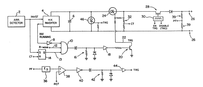
The ;?resent cardic~verting Ey t@m
is depicted ~hematically ~ Fi~ The
~ystem includes ~ nu~ber o~ cir~uit el~ment~ ~o~mon to
Vnited State~ P~tent N~. 4,614,192 and ~lgned to the
~ame ass~gnee ~6 the in~tant ~ppll~t~Gn.
An ~rrhythmia detector ~ircu~t ~ uple~
with i~plAnt~le ele~troaes ~not shown) that ~r~ n
/, ~
~'?~ 3
-5-
turn, connected with the heart of a patient. The
arrhythmia detector circuit 2 is capable of detecting
an arrhythmic condition and providing an INVST output
signal thereupon. The arrhythmia detecting circuit 2
may include a heart rate detector circuit and a
probability density function ~PDF) circuit such that
when the heart rate exceeds a predetermined threshold,
and the probability density function conditions are
satisfied, the INVST signal is issued to a high-voltage
inverter and control circuit 4. The rate analysis and
PDF circuits are described in the copending Imran et al
application. It should be apparent that other schemes
for detecting an arrhythmia may be employed to provide
a start signal (or INVST signal) to a high-voltage
inverter circuit 4.
The high-voltage inverter 4, also known as a
DC-to-DC converter, is a conventional element well
known in the implantable defibrillator art. Reference
should be made, for example, to U.S. Patent No.
4,164,946, which describes the DC to-DC converter
telement 30 in the '946 patent). Upon receipt of the
INVST signal, the high-voltage inverter 4 charges an
internal energy storage capacitor 6 which is charged to
a predetermined level. When the high-voltage inverter
4 begins operation upon receipt of the INVST signal,
the high-voltage inverter begins running, or charging,
the capacitor 6, and provides an INV RUNNING signal
through inverter logic element 8, which is connected to
an input of AND gate 10.
The AND gate 10 has two additional inputs.
6 ''. ~
Input 12 is from an R-wave detector as dlsclosed in the
copending Imran et al application. Upon detection of
each R-wave, a signal is provided to input 12 of the
AND gate 10. Input 13 of the AND gate 10 is from
flip-flop 14, which is set upon receipt of the INVST
signal from the arrhythmia detector 2. The flip~flop
14 is reset upon receipt of a CT signal r to be
described below.
Upon the detection of an arrhythmic condition
and the issuance of an INVST signal, the high-voltage
inverter starts running and issues an INV RUNNING
signal which is inverted by inverter logic element 8 to
provide a low input to the AND gate 10. When the
inverter stops running, l.e., at the completion oE the
charging of the storage capacitor 6, the output of
inverter logic element 8 goes high. A subsequent
R-wave input to the AND gate 10 causes a pulse to be
emitted, througn a suitable RC pulse-shaping network 16
and buffer 18 to a transistor 20. The transistor 20 is
then actuated and a patient trigger pulse (TRIG) is
applied over lead 22 to fire a patient SCR 24. Upon
the firing of patient SCR 24, the fully charged
capacitor 6 is then capable of discharging across leads
26 which are connected to the electrodes tnot shown)
associated with the heart of a patient.
Connected in series between the capacitor 6
and the electrode lead terminal~ 26 is a power field
effect transistor (FET) 28. The power FET 28 is
coupled with a clock pulse generator 30 which provides
high-frequency clocking pulses to the gate of the FET
-7- ~ 2
28. The clocking pulses are provided to the FET 28
upon receipt o a T~IG siynal when the transistor 20 is
turned on.
The clocking pulses from the clock pulse
generator 30 serve to turn the power FET on and off at
a high frequency, in accordance with the frequency of
the clocking pulse generator 30. Preferably, the clock
pulse generator 30 provides actuating pulses to the FET
28 at a frequency at least equal to 1 K~z and
preferably between 10 KHz and 1 MMz.
Thus, the TRIG pulse from transistor 20 turns
on SCR 24 and enables the clock pulse generator 30.
The capacitor 6 then discharges across the electrode
leads 26, at a fre~uency proportional to the clock
pulse frequency from the clock pulse generator 30. A
pair of resistors 32 connected in parallel with the
terminals 26 detects the discharge via the CT lead.
This CT lead is connected to the reset terminal
of flip-flop 14 and, upon detection of the discharge, a
CT pulse resets the flip-flop.
Also connected in parallel across the
electrode leads 26 are a pair of resistors 34 which
detect the pulse discharge applied across the electrode
leads 26. This puIse feedback signal (PF signal) is
provided to an envelope detector 36. The envelope
detector 36 detects the envelope of the high-frequency
~xponentially decaying pulses and provides the detected
envelope signal to a positve input terminal of a
comparator 38. The comparator 38 has a negative
terminal coupled to a reference voltage. When the
~ 3 ~
voltage of the detected envelope drops below the
reference, the comparator 38 provides an output which
is inverted by inverter 40, shaped by pulse-shaping
network 42, through a buffer 44, to provide a TRG
signal. The TR5 signal is provided to a disable
terminal of the clock pulse generator 30 to stop the
clock pulse generator from delivering further clock
pulses to the FET 28. The TRG signal is also provided
to a truncate SCR 46 to fire the truncate SCR 46. When
the truncate SCR 46 is fired, the exponentially
decaying pulse across the electrode terminals 26 is
truncated or shorted so that no further energy is
delivered to the electrodes. This is done since it is
undesirable to require the pulse to exponentially decay
to a zero level, as was stated in the copending Imran
et al application.
In operation, detection of an arrhythmic
condition by the arrhythmia detector 2 initiates the
running of the high-voltage inverter circuit 4. When
the inverter circuit completes its charging of the
capacitor 6, and, upon receipt of an R-wave via lead
12, the AND gate lO is asserted and a trigger pulse
(TRIG pulse) is issued by transistor 20 to fire the
patient SCR 24 and to enable the clock pulse generator
30. Tne capacitor 6 then discharges across the
electrode lead terminals 26 and the exponentially
decaying wave form is chopped by the high-frequency
actuation of the power FET 28.
Fig 2(a~ depicts the chopped exponentially
decaying wave form in exaggerated form. In essence,
g
the wave form of Fig. 2(a) is a wave packet comprising
a plurality of high-frequency cardioverting or
defibrillating pulses that are applied across the
electrode leads 25. Fig. 2(b) depicts an exponentially ~,
decaying wave form that is not chopped in accordance
with the present invention and thus is s:imilar to the
type of pulse delivered in prior defibrillating
systems.
Above, a preferred embodiment of the present
invention is disclosed. It should be appreciated,
however, that the present invention is not limited to
the specific embodiment disclosed herein, but solely
with reference to the following claims.