Note: Descriptions are shown in the official language in which they were submitted.
1 3 1 9 1 78
Controllable AC Voltage Amplifier
The present ;nvention relates to an AC voltage
amplifier, particularly a wideband amplif;er for optical
communication, comprising a single-gate field-effect
transistor to which the input voltage to be amplified is
applied at the gate end.
There are prior-art AC voltage amplifiers containing a
dual-gate field-effect transistor which operates in a
frequency range of a few hertz to several gigahertz.
A dual-gate f;eld-effect trans;stor can be thought of as
a cascode circuit represented by two single-gate
trans;stors, with the input transistor used in a
common-source configuration and the output transistor
operating as a gate stage in the turn-on region. ~ecause
of its complicated geometrical structure, a dual-gate
field-effect transistor has a lower cutoff frequency
than a singLe-gate field-effect transistor used as part
of a dual-gate field-effect transistor, and it has a
higher input capacitance than such a single-gate
field-effect transistor. In a dual-gate field-effect
transistor, small currents may occur in the control
process which also flow in the gate stage. As a result,
the cutoff frequency is reduced.
-1.
1 3 1 9 1 ~ 8 7243~-89
This AC voltage amplifier does not permit a very large bandwidth
and a wide dynamic range.
It is an object of the invention to provide an AC
voltage amplifier which is controllable and does not have the
disadvantages of an AC voltage amplifier with a d~tal-gate field-
effect transistor.
It is another object of the invention to provide a
controllable multiple-stage amplifier.
The first-mentioned object is attained by arranging that
a first voltage derived by a resis~-ance-capacitance combination is
~- - applied to the single-gate field-effect transistor at the gate end
and a second voltage at the drain end, that the second voltage is
opposite in sign to the first voltage, and that the gain of the
single-gate field-effect transistor is controllable through the
second voltage.
It is advantageous that for the single-gate field-effect
transistor, any field-effect transistor with a high transition
frequency can be used, e.g. a high-electron-mobility transistor
(H~MT).
The invention has the advantage that the load resistance
connected to this AC voltage amplifier is nearly independent of
frequency. While in a cascode circuit as is represented by the
dual-gate field-effect transistor, the cutoff frequency changes
twice as a function of the voltage, according to the invention
only a single transistor of higher cutoff frequency is controlled.
The second-mentioned object is attained by constructing
the multiple-stage amplifier from two or more AC voltage
L .
1 3 1 9 1 78 72~30-89
amplifiers according to the invention, each amplifier comprisiny a
single-gate field-effect transistor and forming one stage.
In a further embodiment, the single-gate field-effect
transistors of the individual stages operate at a nearly constant
drain-source voltage. They are driven by transistors acting as
current sources with a variable drain current in the pinch-off
region of the drain-source voltage; the drain current depends only
on the voltage with which the transistors are driven.
The invention may be summarized, according to one aspect
as a broadband amplifier for amplifying AC voltage, comprising: a
single-gate field-effect transistor, connected in a common source
configuration, having a gate terminal, a source terminal and a
dr~in terminal, the input voltage to be amplified being applied to
the gate terminal and the source terminal of the single-gate
field-effect transistor being directly connected to ground; first
means including a resistance-capacitance combination for
connecting a first voltage source to the gate terminal of the
single-gate field-effect transistor; and second means for
connecting a variable second voltage source, opposite in sign to
the first voltage, to the drain terminal of the single-gate field-
effect transistor; wherein the gain of the single-gate field-
effect transistor is controllable through the variable second
voltage.
According to another aspect, the present invention
provides a multiple-stage broadband amplifier comprising5 at least
two AC voltage amplifiers connected in series, each AC voltage
amplifier forming one stage of the broadband amplifier and
1 3 1 9 1 7~ 72430-89
comprising a single-ga~e field-effect trans:istor having gate,
drain and source terminals and being connected in a common source
configuration, the gate terminal of the single-gate field-effect
transistor of the first AC voltage amplifier in the series being
connected to an input voltage to be amplified; and a controllable
power field-effect transistor, wherein a first voltage is derived
by a resistance-capacitance combination and is applied to the gate
terminal of the single-gate field-effect transistor of each stage,
the single-gate field-effect transistor of each stage having its
drain terminal grounded through a resistor, and the single-gate
field-effect transistor of each stage being controllable at its
respective source terminal through the drain current of the
controllable power field-effect transistor.
According to yet another aspect, the present invention
provides a multiple-stage broadband amplifier comprising: at least
two AC voltage amplifiers, each amplifier forming a stage of the
broadband amplifier and comprising a single-gate field-effect
transistor having gate, source and drain terminals; and at least
two bipolar transistors, each connected to a respective single-
gate field-effect transistor; wherein a first voltage is applied
to the drain terminal of the single-gate field-effect transistor
of each stage, a second voltage is applied to the drain terminal
of each of the single-gate field-effect transistors in a variable
manner via a resistor and one of the at least two bipolar
transistors which is connected to the respective stage, and the
drain-source voltage of each of the single-gate field-effect
transistors is adjustable by means of the first voltage via a
3a
.~
1 3 1 9 1 78 72430-89
plurality of resistors.
The invention will now be explained by way of example
with reference to the accompanying drawings, in which:
Figure 1 shows the principle of the amplifier circuit
3b
1 3 1 9 1 7 8 72430-89
wlth a single-gate field-effect transistor in
a common-source confiyuration;
Fig. 2 shows an embodiment of the amplifier in a
single staye containing the single-gate field-
effect transistor of Fig. 1 and an additional
field-effe~t transistor for providing voltage
drive;
Fig. 3 shows a multiple-staye amplifier consisting of
four stages each containing a single-gate
field-effect transistor as shown in Fig. 2 and
C
3~
" ~319178
of the f;eld~effect trans;stor for driv;ng the
drain of the s;ngle-gate fie~d-effect transistor;
Fig. ~ shows a mu~t;ple-stage amplifier consisting of
four stages each containing a sing~e-gate
field-effect transistor as shown in Fig. 2 and
of the fie~d-effect transistor for driving the
source of the single-gate field-effect
transistor, and
Fig. 5 shows a multiple-stage amplifier consisting of
four stages each containing a single-gate
fieLd-effect trans;stor as shown in FigO 2 and a
bipolar transistor as a current source for
driving the drain of the s;ngle-gate
f;eld-effect transistor.
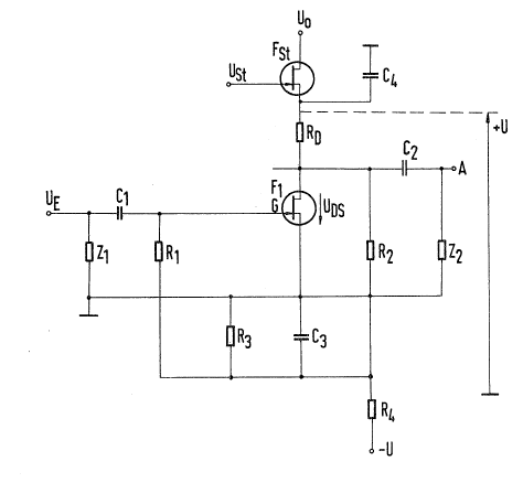
The basic circuit diagram shown in Fig. 1 contains a
single-gate field-effect transistor F1 used in a
common-source configuration. A high-frequency AC voltage
UE is applied to its gate through a capacitor C1,
and a negative, constant voltage -U through a resistor
R1. A resistor Z1 represents the input res;stor of
the circuit. It is coupled to the gate of the transistor
F1 through the capacitor C1. A resistor Z2 forms
an output load resistor and is connected to the drain
terminal of the transistor F1 through a capacitor
C2. A positive, variable voltage +U is applied to the
drain of the transistor F1 through a decoup~ing
resistor RD. At higher frequencies~ the resistor RD
may be replaced by a wideband coil; it also serves to
set the gain.
1319178
The fact that the voltages +U and -U are positive and
negative, respectively, applies only in the case of an
n-channel singLe-gate field-effect transistor F1; in
the case of a p-channel transistor, they must have
opposite polarities.
~ecause of the capacitor C2, the output voltage UA
contains no DC component, either.
Fig. 2 shows an amplifier stage which, in addition to
the resistors R1, RD~ Z1' Z2 and the capacitors
C1, C2, contains a capacitor C3 and resistors
R2, R3, R4, w;th which the stage is
voltage-stabilized. In this manner, part of the
drain-source voltage UDs, together with the voltage
-U, here a supply voltage, ;s fed into the gate of the
singLe-gate f;eld-effect transistor and an optimum gate
voltage is set at the transistor. A capacitor C4
between the resistor RD and the source terminal of an
add;tional field-effect transistor FSt is grounded, so
that only a DC voltage is appl;ed at the source
terminal.
In this case, the positive voltage +U is controlled
"wattlessly" by the field-effect transistor FSt, whose
drain terminal is connected to a constant voltage UO,
while ;ts gate is driven by a drive voltage Ust.
The field-effect trans;stor FSt acts as a voltage
source in this case. If the voltage UO ;s applied at
the source end rather than the drain end, the
field-effect transistor FSt acts as a current source.
Instead of a transistor FSt, any other voltage or
current source permitting control of the voltage +U can
be used. The voltage Ust may be generated in a
1 3 1 9 1 78
feedback control loop in which a comparison between the
reference value and the actual value of the output
voltage UA is performed.
A change ;n the voltage +U by means of the field-effect
transistor FSt has the effect that the drain current
ID of the single-gate field-effect transistor F1 is
also varied. The latter then operates in a region of
variable transconductance
D
and variable gain.
Instead of the voltage drive provided by the
field-effect transistor FSt, current dr;ve can be
provided by a current source.
.
A resistor R5 suppresses high-frequency oscillations.
A multiple-stage amplifier (Fig. 3) cons;sts of four
stages each containing a single-gate field-effect
transistor F1, Fz, F3~ F4 having its drain
terminal connected through a resistor RD to the source
terminal of the field-effect transistor FSt, so that a
variable positive voltage +U is applied to all
single-gate field-effect transistors F1 through F4.
In this manner, the dynamic range of each of the
single-gate field-effect transistors F1 through F4
is fully utilized.
All resistors R3, Z1~ Z2 have been eliminated
except the resistor Z1 in the first stage. The
capacitor C2 at the drain of the single-gate
131ql7~
field-effec-t transistor in each stages has merged w;th
the capacitor C1 at the gate of the respec~;ve next
stage.
Two capac;tors CA, C~ at the input end and two
capacitors C4, C3 in each stage connect the AC
voltage to ground.
The single-gate field-effect transistors F1, F2,
F3, F4 of another, l;kew;se four-stage amplifier
(Fig. 4) are driven at their sources by the drain
current of an n-channel enhancement-mode metal-oxide
semiconductor field-effect transistor (MOSFET)~ The
latter is driven by a drive voltage Ust. A capacitor
C5 at the source of each of the single-gate
field-effect transistors F1 through F4 provides AC
voltage isolation.
A supply-voltage source provides a negative, constant
supply voltage -U, which is applied to the gate terminal
of each of the field-effect transistors F1 to F4
through a resistor R6 and the res;stor R5. Each of
the drain resistors RD is connected in parallel with a
resistor R9 and grounded.
With the aid of the supply voltage -U and the voltage
div;der formed by the resistors R2, R9, the
negat;ve, constant gate voltage is generated.
A resistor R8 forms the ;nput resistor of the
amplifier circuit.
A third four-stage amplifier ~Fig. 5) contains pnp
bipolar transistors T~ to T4 used in a common-base
configuration. Each of them drives the drain of a
single-gate field-effect transistor F1 to F4 via the
~319178
associated resistor RD. The bases of the transistors
T1 to T4 are preceded by resistors R10; they are
grounded through a capacitor C6. The base voltage is
provided by the collector of a drive transistor TSt,
whose base is driven by a voltage Ust and whose
emitter is grounded through a resistor R13.
The constant voltage +U is applied to the emitters of
the transistors T1 to T4 through emitter resistors
R11 and to the collector of the drive transistor TSt
through a collector resistor R12. The gate voltage is
derived via the resistors R1, R2, R4. The
constant, negàtive voltage -U is grounded through the
capacitor C4. The gate of each of the field-effect
transistors F1 to F4 is grounded through the
resistors R1, R5 and a capacitor C7.
Through the capacitor C1, the AC voltage UE is
coupled into the multiple-stage amplifier. A resistor
R14 represents the input resistor of the
multiple-stage amplifier.
In this c;rcuit, the drain-source voltage UDs of the
single-gate field-effect transistors F1 to F4 is
adjusted so that it lies in the pinch-off region; then,
the drain current can be impressed (on the transistors
T1 to T4) nearly independently o, the drain-source
voltage UDs.
Instead of the transistors T1 to T4, field-effect
transistors or Darlington pairs can be used in the
network.
1319178
In the four-stage ampl;fiers shown, a dynamic range of
up to 40 dB is possible in the GHz region. Since each
stage is dr;ven separately, the overload behavior is
favorable.