Note: Descriptions are shown in the official language in which they were submitted.
1319196
Applicant :
PENTASYSTEM S.p.A.
Via Calepina, 50
38100 TRENTO (Italia)
"CARD OR PASS IN PLASTIC MATERIAL INCORPORATING AN INTRGRATED
MEMORY CIRCUIT"
_ !
The present invention relates to a card or pass in plastic
material incorporating an integrated memory circuit and an
univocal optical code for identification of the card. At present
such supports are for instance widely used for credit cards,
5. automatic cash-point cards and identification passes.
Such a memory support is useful in all those cases where high
data safety and protection against frauds resulting from unlawful
manipulation are required. In particular it is very usefully
utilised for electronic memory credit cards, where data safety
lO. and small dimensions of the electronic device are fundamental to
the reliability of the product.
The data protection devices presently available are obtained by
providing in the card a further device (normally a single chip
microprocessor suitably programmed) which works as a filter
' 131qlq6
-- 2 --
between the memory and the outside world. This device or
microprocessor can also be on the same silicon chip which houses
the memory matrix. Such arrangement entails all a series of
drawbacks. First of all the microprocessor occupies a consider-
5. able area of the silicon chip, with the consequence of increasingconsiderably the cost of the device. In the second place the
microprocessor requires all a series of interfacing signals
towards the external world (clock, reset...) which necessarily
complicate the connection with the writing/reading devices. And
10. in the third place the program- contained on the ~icroprocessor
can be read by using suitable techniques, thus making the system
less safe.
The presently available cards or passes, of the type to which the
present invention applies, foresee more than four external
15. electric contacts, on two rows, for connection with the internal
circuit. Since the electric and mechanical relialibity of such
devices is in inverse ratio to the number of connecting
contacts, the assembly is of poor reliability during usage.
Moreover the writing and reading devices to be used with this
20. support are complex and expensive owing also to the intrinsical
difficulty of carrying out contact means which keep a good
alignment in the course of time.
Aim of this invention is therefore to carry out a credit card or
similar extremely strong, that is as flexible and capable of
25. standing wear and tear as much as possible, which allows for
protection of the data contained in an electronic memory, not
including programmed logic, against access and/or alteration
attempts from unauthorized persons, and to allow the reading
and/or writing with devices less complicated than the existing
30. ones.
,. .. .
' 1 3 1 9 1 96
- 3 -
The above aim has been reached by providing a support comprising
an integrated memory circuit of EEPROM technologywhich is
connected with the outside only through four contacts and
containing voltage conversion circuits able to generate internal-
5. ly, starting from a single voltage (for instance 5 volts), theone necessary to the programming of the memory cells, with the
consequence that the integrated circuit works with a single
feeding voltage, being provided that through one of the contacts
goes an input signal (for instance at 5 volts in continuous
10. current + 5%), that through another contact a connection with the
input outgoing line is foreseen, that a logical type signal
passes through a further contact and acts as clock signal for
data and instructions, that an open drain twodirectional line
(SDA) passes through a fourth contact which acts as support for
15. data and instructions. Preferably the signals have the logical
"zero" included between -l V and 0,8 V and the logical "one"
included between 2 V and VCC + 0,5 V.
.
An improvement provides for the integrated memory circuit to have
an asynchronous ~erial interfacing on two wires and to contain
20. the necessary circuits for handling a feeding protocol with an
external writing and/or reading device, for handling the writing
timings, for the random access to any memory byte and for any
other operation which might by required.
A further improvement provides for the integrated memory circuit
25. to be implemented with a digital filter to filter the disturbanc-
es which may be present on the communication lines with the
external world.
Another improvement, still, foresees that the four contacts are
1 3 1 q 1 q6
-- 4 --
arranged on a single line, so as to increase the resistance of
the card to mechanical stress. In this case provision is made
also for the contacts to be connected to the integrated unit in
such a way to be on a single si.de of it.
5. A further improvement provides for the thickness of the seat
which receives the portion of the integrated circuit to be bigger
than the thickness of the integrated circuit and that the only
support of the integrated circuit are the four tracks coming out
from one side only, so that the integrated circuit can slightly
10. move inside said seat while the support is bended, with no damage
to the connecting tracks or to the integrated circuit itself.
Provision can also be made for each card to have an internal code
inside the card itself, said code being utilised as a component
of the entry key to the information contained in the integrated
15. circuit. Preferably this internal code is of the optical type
and the card support is transparent to infrared rays.
It is also foreseen that the internal code ~ay be inserted in
the card by means of two different codification systems, one
being the logical complement to the other, so that the
20. alteration, for instance by adding on the surface ink opaque to
infrared rays, of an area carrying the code written in the first
codification system, obliges a forger to carry out a correspond-
ing alteration on the other area, i.e. the removal of part of the
ink forming the code written in the second codification system,
25. which is impossible without destroying the support incorporating
the code written in the two complementary codification systems.
Further characteristics and advantages of the support according
1 3 1 q 1 9~
-- 5 --
to the invention will be better illustrated with reference to the
following description and to the enclosed drawings, wherein :
Fig. 1 shows a view of one face of the card or pass according
to the invention;. Fig. 2 shows a view of the other face of the card or pass
according to the invention;
Fig. 3 shows a variation of the internal side of a layer
forming the card or pass, duly treated;
Fig. 4 shows a view in enlarged section of the card or pass
10. according to the invention;
Fig. 5 shows an enlarged detail of the section of the card
or pass of Fig. 4; and
Fig. 6 shows an enlarged top view of the group: integrated
circuit - connecting tracks - supporting film.
15. The card or pass 10 according to the invention consists of
various layers of shock-resistant plastic film transparent to
infrared light, engaged to one another for instance by thermo-
pressure welding. Inside these layers 15a and 15b a seat is
provid0d for an integrated memory circuit 22 externally connected
20. by means of four small electrical contacts, 11, 12, 13 and 14
respectively. On the lower face of the card (Fig. 2), a band 16
of magnetizable material, suitable for supporting information and
compatible with the reading and writing systems presently used,
can be applied. The magnetic band 16 is positioned on the paper
25. in conformity with ISO standard or in any other area it needs to
be placed. The magnetic band can be obtained both by smearing of
magnetic ink and by applying a suitable magnetic strip.
On the internal faces of one of the layers (according to the
1 3 1 9 1 96
embodiment of Fig. 3 and 4) optical codes are printed along the
portions indicated respectively with 18a and 18b by means of ink
opaque to infrared rays. These optical codes can be read in
transparency by means of an infrared light source and an optical
5. detector working on the same wavelength. By means of these codes
the marking of a particular code on each card is done during its
manufacturing, thus making each card different from all the
others.
For instance, a feasible way to prevent tampering of the optical
10. code foresees the printing in the two different areas 18a and 18b
of an identical code, for instance a number, by two different
codification systems, one being the logical complement of the
other. The reading device will allow access to the information
only after verifying whether the same code is present on both
15. areas 18a and 18b. A forger who would want to alter the code
would have to change both the ar~as, one complementary to the
other, so as to keep their congruity unaltered.
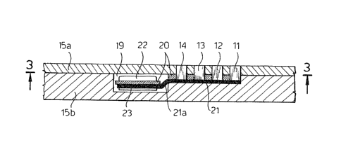
With reference to Fig. 4, 5 and 6, between layers 15a and 15b, a
seat 19 is foreseen internally inside which an integrated circuit
20. 22, covered by a suitable anti-dampness resin 23 and supported by
metallic tracks 21, is placed. The metallic tracks are kept
together by means of a kapton film 20; they come out from only
one side of the integrated circuit and in their bending area 21a
are free, i.e. not connected to the kapton film (Fig. 5 and 6).
25. Such an arrangement allows, in the case of bending and/or
twisting of the card, a good chance of movement to the integrated
circuit inside seat 19, without the presence of destructive
mechanical stress which would occur should the tracks 21 come out
i~rom various sides of the integrated circuit 22, or in the case
131ql96
-- 7 --
they were coupled to the film 20 in the bending area. The
contacts 11, 12, 13 and 14 are welded to the tracks 21 thanks to
the latter particular shape, i.e. free on both sides in the
welding area 21b. (Fig. 6). In the contrary case the presence of
5. the kapton film would make a strong welding a problem. The
integrated circuit is a memory capable of storing information
even without feed and allowing its subsequent change by means of
electrical signals. The memory capacity of the integrated circuit
depends on the specific use and on the integrated circuit chosen.
10. Data retention capacity, without alteration of the information,
is at least 10 years. The technology of the integrated circuit is
the EEPROM one with a voltage converter on the chip capable to
generate the programming voltage. In addition, a digital filter
is implemented on the integrated circuit to clear the clock and
15. data lines from external disturbances, thus increasing the safety
of the data transmitted and/or received.
According to the invention, with the integrated circuit used, the
interface between the memory and the outside world is o~ the
serîal type. The connection with the outside is through metallic
20. contacts 11, 12, 13 and 14. The contacts have an approx. 1.76 mm
x 2.86 mm. dimension.
Fig. 5 shows enlarged seat 19 which receives the film portion and
the integrated circuit. In seat 19 the integrated circuit can
move as free interspaces 40 and 41 are foreseen in front of the
25. lower and upper sides of the support. The integrated circuit has
thus a certain moving space in case the card is bent. The area
of the contacts 11, 12, 13 and 14 on the contrary is foreseen
without interspaces which could allow oscillations, thus insuring
always a constant contact.
1319196
At least on the portions of layers 15a and 15b which come into
contact with the metallic tracks 21, an anti-static treatment can
be foreseen, for instance by depositing conductive lacquers.
With reference to Fig. 1, a particular electric signal is related
5. to each contact 11, 12, 13 and 14. More precisely, according to
the preferred embodiment, colltact 11 is related to the input
incoming line at 5 Volts (VCC); contact 12 is related to the
input outgoing line (VSS), contact 13 is related to the incoming
line of the data synchronizing clock (SCI); contact 14 is related
10. to the two-directional line of the serial data (SDA). The typical
working parameters for each signal in correspondence to the
contacts are preferably the followings :
VCC: + 5 V in direct current + 5%;
VSS: O V;
15. SCL: signal which has the logical zero comprised between -1 and
+0,8 V and the logical one comprised between 2 V and VCC + 0.5 V.
The frequency field allowed is between 0 and 100 kilohertz. The
duration of a low half~cycle is not inferior to 4.7 microseconds,
and of a high half-cycle is not inferior to 4 microseconds.
20. SDA: represents the two-directional line at open drain having
the same electrical characteristics of signal SCL.
The logical zero included between -1 V and +0.8 V is also defined
as low logical level.
The logical one included between 2 V and VCC + 0.8 V is also
25. defined as high logical level.
With the foreseen four contacts we have a communication protocol
between the integrated memory circuit and the reading/writing
device which works as follows :
131ql96
the reading/writing device gives the clock signal for data
transfer from and to memory.
The SDA line can change status only while SCL is low. Status
variations of SDA while SCL is high are only to indicate STARr
5. and STOP conditions.
According to said protocol, all the controls are preceded by the
START condition consisting in a transition from high to low of
SDA while SCL is high. All communications end with a STOP
condition consisting in a transition from low to high of SDA
10. while SCL stays high.
- The data receiving device, after having received eight data or
command bits informs the transmitting device of the acceptance;
to do so during the ninth clock cycle the receiver puts the SDA
line low starting an identification. The absence of such
15. identification indicates that the receiving device is engaged and
the operation is to be tried again.
It is foreseen that the data and/or control bytes are sent out
starting from the most significant bit.
A group consists of eight bytes where the first byte is in a
20. memory location of multiple of 8 address. At START condition,
memory selection is carried out by means of a word of eight bits
formed by 1, O, 1, O, A2, A1, AO, RW where A2, A1, AO indicate
which page of 256 bytes will be interested in the subsequent
operation, RW indicates whether the subsequent operation will be
25. a reading (RW = 1) or writing (RW = O) one and is the less
significant bit of the selection word.
For the writing operation of 1 byte, the memory requires a second
13191q6
-- 10 --
address field of 8 bits, which specifies which one of the 256
memory cells of the selected page will be used, following by the
value (1 byte) to be written in the memory and by the STOP
condition.
5. If instead we want to procede to the writing operation of a group
the process is similar to the 1 byte writing operation, supplying
as address the one of the group first byte, followed by 8 data
bytes and by the STOP condition.
In the reading operation the communication starts as per the
10. writing operation with the difference that the RW bit of the
selecting word is placed on 1.
For the reading of any memory cell, according to the protocol, a
fake writing operation must be first carried out, i.e. an
operation where the address is sent without the data byte. This
15. operation is used to select the address of the byte which is to
be read. Subsequently the protocol sends the selection command
with RW = 1 and, by keeping on generating the clock signal, it
receives the desired byte from the memory. If, according to the
protocol, we keep generating the clock signal, the memory keeps
20. sending new bytes, increasing the memory address from which they
are taken. If the memory address goes over the limits of the 256
bytes page, the address is put to zero so that the bits selected
later on are taken starting from the beginning of the same page.
The operation ends with a STOP condition.
25. It is eviclent that this communication protocol insures that the
exchange of data with the outside is through four contacts only.
We have anyhow a circuit support which guarantees a greater
J
' 13191q6
working reliability as compared to the exis-ting ones and which
can be mass produced. Moreover, with such an arrangement, a
unique external input ~t +5 V is foreseen.