Note: Descriptions are shown in the official language in which they were submitted.
131~271
PROGRAMMABLE CONTROLLER WIT~ FIBER OPTIC
INPUT/OUTPUT MODULE
The field of the invention is programmable controllers
such as those described in U.S. Patent Nos. 3,810,118;
3,942,158; 4,165,534 and 4,442,504 and particularly fiber
optic input/output modules for such controllers.
Background of the Invention
Programmable controllers are typically connected to in-
dustrial equipment, such as assembly lines and machine
tools, to sequentially operate the equipment in accordance
with a stored program. In programmable controllers such as
those d sclosed in the above cited patents, for example, the
control program is stored in a memory and includes instruc-
tions which are read out in rapid sequence and executed to
examine the condition of selected sensing devices on the
con~rolled equipment, or to energize or deenergize selected
operating devices on such equipment contingent upon the
status of one or more of the examined sensing devices.
The processor for these controllers is designed to
rapidly execute programmable controller type instructions
which in medium to large sized controllers includes not only
instructions that manipulate single-bit input and output
data, but also arithmetic instructions, file handling in-
structions, timers and counters, sequencers and other, more
complex instructions. Such instructions have become quite
standardized in the industry and they may be directly associ-
ated with elements of a ladder diagram which is easily
understood by control engineers. Program panels such as
those disclosed in U.S. Pat. Nos. 3,798,612 and 3,813,649
--1--
13~271
and in U.S. Pat. No. 4,070,702 have been developed to assist
the user in developing and editing ladder diagram type con-
trol programs comprised of such programmable controller in-
structions. To insure that the programmable controller can
respond quickly to change in the status of sensing devices
on the controlled system, it is imperative that the control-
ler execute the control program repeatedly at a very high
rate. The rate at which a programmable controller can exe-
cute the instructions in its instruction set, as well as the
size of the control program, are the primary factors which
determine the rate at which the programmable controller can
repeatedly execute, or "scan", ,the control program.
The sensing devices that are interfaced to the pro-
grammable controllers detect various conditiGns or states of
the e~uipment being controlled and provide input data for
use by the ladder program. In response to the sencor data,
the program causes the actuators to activate and deactivate
various parts of the equipment. The sensors typically are
switches, such as limit switches that open or close as a
part of the machine or a workpiece passes by the sensor.
The status of the switch, open or closed, is represented in
the programmable controller 2S a high or low level voltage
which may be digitally processed as a logical one or a zero.
In certain environments electrical signals are hazard-
ous, such as in chemical processes where a spark could cause
an explosion. Therefore, fiber optic control systems have
been considered for use in such environments. A fiber optic
sensing system could send light from a remote source through
a fiber optic cable into 'he hazardous environment. There a
shutter type sensor can transmit or block the flow of light
into a second fiber optic cable in response to the sensed
13192~1
condition. The second cable is coupled to a I/0 module of
the programmable controller.
As with other types of sensor systems, the optical link
and its various components degrade over a period of time.
The optical -ouplings and the sensors may increasingly
attenuate the light transmission with time which, if allowed
to continue, can result in a failure of the sensor link. A
technique is reguired to dynamically monitor the fiber optic
sensor link and provide an indication of the onset of its
degradation so that the faulty components may be replaced
before a catastrophic failure occurs.
SummarY of the Invention
A system for evaluating the ~uality of an optical
communication link, such as a fiber optic cable, transmits
light over the link at various in ensities. The evaluation
is made based on which intensities are received at the other
end of the link.
The system comprises a transmitter for sending infor-
mation over the communication link at several light levels.
A receiver is coupled to the link for receiving the trans-
mitted information. Circuitry is provided for determining
which of the light intensities were received. Based on that
determination the system evaluates th~ light attenuation and
thereby the quality of the communication link.
The present invention provides a mechanism for periodi-
cally testing the link and detecting when maintenance should
be performed on the link.
~31~71
In accordance with an embodiment of the
invention, a communication system employing an optical
communication link, the system is comprised of a
transmitter for transmitting a plurality of predefined
S intensities of light through the communication link and
including two power terminals, a light source coupled to
the communication link and having a first terminal
connected to one of the power terminals and a second
terminal connected to a node, and apparatus for
lo selectively connecting different impedances between the
other of the power terminals and the node to selectively
apply at least two different magnitudes of electric
current to the light source; an apparatus for receiving
the light transmitted through the communication link;
apparatus, coupled to the apparatus for receiving, for
determining for which ones of the plurality of predefined
intensities light is and is not received; and apparatus,
responsive to the apparatus for determining, for
evaluating the attenuation characteristic of the optical
communication link.
In accordance with another embodiment of the
invention, an input/output system for connecting a remote
device to a programmable controller via a fiber optic
communication link, the input/output system is comprised
of apparatus for transmitting light to the remote device
through the fiber optic link at a plurality intensity
levels and including two power terminals, a light source
- 3a -
.. :- ,,.
. , .
131~27~
having a first terminal connected to one of the power
terminals and a second terminal connected to a node, and
apparatus for selectively connecting different impedances
between the other of the power terminals and the node;
S apparatus for receiving light returned by the remote
device via the fiber optic link; apparatus, eoupled to
the apparatus for receiving, for determining for which
ones of the plurality of transmitted light intensities
light is and is not received from the remote deviee; and
apparatus, responsive to the apparatus for determining,
for evaluating the attenuation eharaeteristie of the
fiber optic eommunieation link.
In accordance with another embodiment, a
communication system employing an optical communieation
link, the system is comprised of a transmitter for
sending a unique multiple bit digital signal through the
optical communication link at each one of a plurality of
light intensities; a receiver coupled to the optical
eommunieation link for reeeiving light therefrom;
apparatus, coupled to the receiver, for determining which
of the plurality of light intensities are reeeived by
deteeting the unique multiple bit digital signals; and
apparatus for evaluating the quality of the optieal
eommunication link in response to the determination of
which of the plurality of light intensities were
received.
- 3b -
131~271
Brief Description of the Drawings
In the drawings which illustrate the embodiments of the
present invention:
Figure 1 is a perspective view of a programmable con-
troller which employs the present invention;
Figure 2 is a schematic block diagram of the fiber
optic input/output module shown in Figure 1;
Figure 3 is a schematic block diagram of the output
circuit in Figure 2;
10Figure 4 is a schematic block diagram of the input
circuit in Figure 2;
Eigure 5 is a waveform diagram of the optical signal
sent over one of the fiber optic channels;
Figures 6, 7 and 8 are computer program flow charts of
interrupt rou.ines for the microprocessor in Figure 2;
Figures 9a and b are a flow chart of the main computer
program for the microprocessor of Figure 2;
Figure 10 is a diagram of the data structure used by
the interrupt routines and main program; and
20Figure 11 is a truth table for determining the quality
of the fiber optic transmission link.
Detailed Description of ~he Invention
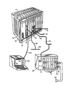
With initial reference to Figure 1, a programmable
controller 10 of the present invention is housed in a rack
12 which includes a series of slots that receive a plurality
of p-inted circuit board modules 16-18. These modules
connect to a mother board which extends along the back
surface of the rack 12 to provide a backpiane 11. The
backplane has a plurality of module connectors which are
electrically interconnected by a conductive pattern on the
-4-
131~271
baGkplane to provide a series of signal buses to which the
modules connect. The rack 12 contains a power supply module
14, a system controller 16, a program execution module 17
and a plurality of remote input/output (I/O) scanner modules
S 18. The remaining locations in rack 12 are empty and the
slots are covered by blank plates until additional modules
are to be inserted in these slots. The physical
construction of the rack 12 is disclosed in Canadian Patent
No. 1,263,895, issued December 12, 1989.
The system controller 16 is connected through
cable 22 to a programming terminal 24 which, for example,
may be of the type as disclosed in U.S. Patent No. 4~326,193
or a personal computer. Terminal 24 may be used to load
instructions into the system controller 16 as well as
monitor its operation. Once the instructions have been
loaded into the system controller 16, and its operation
debugged, the terminal 24 may be disconnected from the
system controller. In addition, the system controller 16
may be connected via a cable 26 to a local area network 28
over which it may receive data and programming instructions,
as well as issue status information and report data to a
host computer. This enables a central host computer or
central terminal to program and control the operatlon of a
plurality of programmable controllers 10 on a factory floor.
The remote I/O scanning modules 18 interface the
controller to external I/O racks 20 via serial I/O networks
such as network 15. Each remote I/O rack 20 has a plurality
of local I/O modules 19 and 30 which are coupled to
individual sensors and actuators on the controlled equipment
- 5 -
1 3 ~ ,T 2 7 1
(not shown). The local I/0 modules 19 provide conventional
electrical I/0 connections which may take many forms and may
include, for example, D.C. inputs or outputs, A.C. inputs
or outputs, analog inputs or outputs, and open or closed
loop positioning modules. The remote I/O rack 20 also
contains an adapter module 21 such as the one described in
U.S. Patent No. 4,413,319 which couples data between the I/0
modules 19 and the scanner modules 18 via the I/0 networks
15. The I/0 racks 20 and networks 15 employ conventional
interface and communication technology.
The user enlers a control program into the controller
10 through either the programming terminal 24 or the local
area network 28. ~he controller 10 is then placed in the
"RUN" mode and it repeatedly executes the stored contrGl
program to operate output devices connected to the I/0
racks 20. Because the condition cf the certain input de-
vices can change may times per second, it is imperative that
the sys~em controller 16 and 'he program execution module 17
have sufficient computing power to execute the stored control
program rapidly. Also because a large number and variety of
input and output devices may be connected to the remote rack
20 to operate a complex machine or process, it is imperative
~hat the control program be deveioped using a programming
language which is easily understood by the user.
In the "run" mode of the programmable controller, the
system controller 16 provides supervisory functions of the
overall operation of the programmable controller 10. In
addition this module 16 handles external communication with
the terminal 24 so tha' ~he operator may monitor the process
13~271
controlled by the system and communication with other pro-
grammable controllers and a host computers via LAN 28.
The ladder diagram control programs are stored and ex-
ecuted by the program execution module 17. This module 17
sends and receives data and commands to other modules via
the backplane 11. Sensor data is received by the programmable
controller I/0 scanner modules 18 from remote I/0 racks 20
and stored in the scanner module memory. As the program
execution module 17 needs sensor data, it reads the input
data image table in the corresponding scanner module 18.
When the program execution module desires to change the
state of a control device on the equipment, it writes a new
control bit or word in the output data image table of the
scanner module 18 that handle3 commands for that device.
The scanner then sends the new control word to the proper
remote I/O rack 20 which in turn changes the state of the
device via the I/0 module 19 to which the device is attached.
kemote module 30 interfaces eight fiber optic cables 31
and 32 to the programmable controller system. Four of the
cables 31 transmit a light beam to remote sensors, such as
device 33, and the other four cables 32, receive the optical
signal response from the sensor. The device 33 has a shutter
which responds to 'he sensed cond_tion to either block or
transmit light between the two cables 31 and 32. Four such
sensor loops may be connected to the module 30. Although
only one fiber optic module 30 is mounted in remote I/0 rack
20, additional modules 30 could be inserted as re~uired in
other slots in place of conventional modules 19 as required.
Alternatively, one fiber optic module 30 may transmit the
light to the sensor 33 and the response cable 32 from that
sensor could be attached to a different module 30 in same or
1319271
another controller system. The fiber optic cables and their
complings define an optical communication control linX.
With reference to Figure 2, the eight lines of the
backplate data bus (DC-D7~ are connected to the fiber
optic module 30 via a standard connector on the module. The
four most significant data bits, D4-D7 are connected to four
Schmitt trigger inverters 36, the outputs of which are
connected to the inputs of a four-bit input data latch 38.
The clock input of data latch 38 is connected to a write
control line from the backplane control buses. The clear
input of the data latch 38 is connected to a reset control
line from the backplane of the remote I/O rack 20. The four
output lines from the data latch 38 are connected to a fiber
optic cable output circuit 40. The fiber optic circuit
drives the light emitting diodes that are connected to the
transmitting fiber optic cables 31.
The details of the fiber optic output circuit 40 are
shown in Figure 3. Each of the four data lines from the
input data latch 38 are coupled to one input of four NAND
gates 71-74. The other input of each of the NAND gates
71-74 is connected in common to a data character transmission
line 50. The output of each of the NAND gates is connected
to a separa.e fiber optic cable d~^iver channels 81-84,
respectively. Each of the driver channels is identical and
only one of them, channel 81, will be described in detail.
The output from the NAND gate 71 is coupled to one input
terminal of three NOR gates 76-78. The other input to each
of the NOR gates is connected to one of the output terminals
of a 2 to 4 digital decoder 80. The decoder 80 responds to
a two-bit digital word at its input terminals to produce a
low level enabling signal on one of the three output terminal
~3~9271
that are connec~ed to the NOR gates 76-78 in each driver.
For example, the first output terminal from decoder 80 is
connected to the each of the first NOR gates 76, the second
output terminal is connected to each of the second NOR gates
77, and the third output terminal of the decoder is connected
to the third NOR gates 78.
The output of the first, second and third NOR gates 76,
77 and 78 are connected to the base of three switching
t-ansistors 86, 87 and 88, respectively. Each of the switch-
ing transistors 86-88 is a NPN type device that has its
emitter connected directly to ground. A resistor 96-98
couples the collector of one of the transistors 86-88,
respectively, to a common no~e 90. A light emitting diode
(LED) 92 has i's cathode connected to the node 90 and its
anode connected to a source of positive voltage. One of the
fiber optic transmitter cables 31 is optically coupled to
each light emitting diode 92 to receive the light generated
by the diode.
The value of each of the resistors 96-98 is selected so
that a different amount of current will flow through each
circuit branch when the corresponding transistor 86-88 is
turned on. For example, the second resistor 97 in each
channel may have a value that is twice that of the first
resistor 96 and the third resistor 98 has a value that is
four times that of the first resistor 96. Therefore, when
the second transistor 87 is turned on the current that flows
through its branch is one-half the amount that flows through
the first branch when transistor 86 is OIl. Similarly, when
'he third transistor 88 is turned on, the current flowing
through its branch will be one-fourth the current that flows
- ~31~271
through the first branch comprising resistor 96 and transis-
tor 86. Each of the branches defines means for turning on
the LED 92 at three different power levels thereby emitting
light into the fiber optic cable 31 having three different
intensities. The three LED drive currents are selected so
that even at the maximum length of the fiber optic link
which may typically be 300 meters to and 300 meters from the
sensor 33, the light intensity at the one-guarter power
level is sufficient to produce a return signal on cables 32
at the I/0 module 30 even for the worst case combination of
component tolerances.
The fiber optic response cables 32 from the various
sensor devices 33 are coupled to a fiber optic input circuit
42 shown in detail in Figure 4. The fiber optic input
circuit 42, comprises four separate input channels, 101-104,
with one of the fiber optic input cables 32 being coupled to
each one of the channels. As the input channels 101-104 are
indentical, only one of them, lOl, will be described in
detail. The response cable 32 from the sensor 33 (Figure 1)
is optically coupled to a photo-detector 106 which has a
response tuned to the wavelength of the light transmitted by
the LED 92 through the fiber optic cables 31 and 32. In
response to the receipt of the light from the response cable
32, detector 106 provides an electrical output signal which
is coupled by resistor 108 to the input of a Schmitt trigger
inverter 110. Pull-up resistor 107 couples the output termi-
nal of the detector 106 to a positive voltage source via
filter circuit 109. A capacitor 112 connects the input of
the inverter llO to ground. The output of the Schmitt
trigger inverter 110 in each of the input channels 101-104
-10-
13~9271
is connected to a separate input of a four-to-one multi-
plexer 114.
Referring again to Figure 2, a microprocessor 46 con-
trols the operation of the fiber optic I/O module 30 via
microinstructions stored in ROM 53 connected to the micro-
processor by data and address buses 54 and 55, respectively,
and by one or more control lines 57. Microprocessor 46 may
be any of several well-known devices such as an 8031 micropro-
cessor manufactured by Intel Corp. Port 3 of the 8031
microprocessor has a serial data output pin (TXD) that is
connected via line 50 to the output circuit 40. This port
also has a serial data input pin (RXD) that is coupled via
line 48 to the output terminal of the multiplexer 114 in the
input circuit 42. Another port of the microprocessor supplies
the power level selection signals to the output circuit 40
on lines 52 and supplies the received channel selection
signals on lines 44 to the multiplexer 114 in the input
circuit 42.
The microprocessor data bus 54 is also connected to an
output data latch 56 which receives a data clocking signal
from the microprocessor 46 via a control line 58. The
output data latch 56 has a data clear terminal which is
coupled to the reset line on the backplane of the remote I/O
rack 17. The data latch 56 provides a temporary storage for
an eight-bit data word which is to be sent on the backplane
data bus of the remote I/O rack for the transmission to the
programmable controller 10. Each of the eight output lines
from the data latch 56 is connected to one input of a separate
output NAND gate 60. The other inputs of each of the output
NAND gates 60 are connected in common to a read input terminal
for the fiber optic I/O module 30 which is connected to the
~3~92~
read control line on the backplane control bus of the remote
I/0 rack 17.
During the operation of the fiber optic I/0 module 30,
whenever the status of the sensor devices 33 is to be detec-
ted, light signals at three different power levels aresequentially sent to each sensor. If the sensor is closed
so that the transmitted light is coupled from the first
fiber optic cable 31 to the return fiber optic cable 32, the
receiver channel of the I/0 module will detect the return
light levels. Depending upon which light levels are received
by module, the degree of light attenuation and thereby the
quality of the fiber optic communication link may be deter-
mined. For example, if only the full power signal is re-
ceived a severe degradation of the link is indicated. To
aid in the receiver detecting the various power levels, the
transmitter sends a different unique signal at each level.
Although any of several forms of unique signals may be used,
the preferred embodiment transmits a different character at
each light intensity (Figure 5). The measure of the fiber
optic link quality is then returned by the I/0 module 30 to
the programmable controller 10 so that an indication may be
sent to the system operator enabling corrective action to be
taken. Such action may include replacing the light emitting
diode, cleaning various optical connectors in the link or
replacing a damaged fiber optic cable.
With specific reference to Figures 2, 3 and 4 when the
programmable controller wishes to interrogate the status of
the sensor devices on the fiber optic links, a data word is
sent to the fiber optic module 30 that is received on the
corresponding data lines D4-D7. Typically, all four of the
sensor devices connected to a given I/0 module 30 will be
13~7~
interrogated together; however, individual sensors or various
combinations of the four devices may be interrogated at a
time. If all four sensors are to be interrogated, a data
word having a one bit in each of the four most significant
bits, D4-D7, is written to that module via the backplane
data bus. Each of these bits is fed via the four inverters
36 to separate inputs of the input data latch 38 which is
then clocked by a signal on the write line of the backplane
causing the four data bits to be stored in the latch 38.
Each of the four bits is then coupled to one of the NAND
ga-es 71-74 in the fiber optic output driver circuit 40.
The microprocessor looks at the status of each sensor
33 sequentially by selecting one of the receiver channels
101-104 at a time and looking for a character at each of the
three power levels. Microprocessor 46 initially switches
the multiplexer 114 to receive the light pattern from one of
the response cables 32 so as to produce an electrical signal
on line 48 representative of the characters received from
that cable.
The microprocessor 46 sends two bits over power selector
lines 52 which when decoded by circuit 80 will enable the
full power level by sending a low level logic signal to each
of the first NOR gates 76 in the transmitter channels 81-84.
The microprocessor also transmits a first unique character,
that is designated as the full power character in Figure 5,
over the transmit line 50. This character is coupled to the
other input of each of the NAND gates 71-74. The NAND gates
that are enabled by the backplane data word pass the micro-
processor data signal to the output that is coupled to the
other input of each of the first NOR gates 76 causing the
output transistor 86 to turn on and off corresponding to the
-13-
131~271
bit pattern of the first character. This supplies a full
power current level signal to all the LED's 92 coupled to
each of the channels causing a full-power light level to be
transmitted over each of the first fiber optic cables 31.
If the corresponding sensor device 33 coupled to each
of the transmitter cables 31 i5 in a closed state, the light
from the first cable will be coupled to the response cable
32 connected to that sensor. Normally, the light transmitted
through the response cable 32 will be detected in the corre-
sponding input channel 101-104 for that cable producing an
output electrical signal at the respective input to the
multiplexer 114 that replicates the transmitted character.
After the full power signal time period the micro-
processor causes decoder 80 to activate only the second NAND
gates 77 in each output channel 81-84. At this time a
different character, designated the one-half power character
in Figure 5, is transmitted over each of the fiber optic
cables 31 but a response signal is received at the micropro-
cessor for only the selected input channel 101-104. After
the half power time period has elapsed, the microprocessor
46 changes the state of the output power decoder 80 to
enable only the third NOR gate 78. At this point in time
the microprocessor transmits a third character over line 50
that is designated the one-~uarter power character. When
this character is coupled through the NAND gates 71-74 and
the third NO~ gate 78, the third transistor 88 will turn on
driving the LED 92 at a third current level which is one-
fourth that of the current level when the LED was driven by
the first branch having transistor 86 and resistor 96. As
with the transmission of the full and one-half power signals,
-14-
2 7 ~
the signal received on the selected response cable 32 is
detected and fed to the microprocessor 46.
After the three power level characters have been trans-
mitted over the first cable link, the next input channel is
selected by multiplexer 114 and the three power level signals
are sent over that link. This process is repeated for all
of the fiber optic sensor links.
The flow charts of the programs for the microprocessor
46 enabling it to carry out the aforementioned process are
shown in Figures 6-9. The switching of the power levels and
the receiver channels are carried out by timed interrupts
For example, every two hundred and fifty microseconds the
microprocessor 46 is interrupted and executes an interrupt
routine, shown in Figure 6 that sequentially selects one of
the receiver channels 101-104 by transmitting the proper two
bits over lines 44 to the multiplexer 114. A flag is then
set in the microprocessor's on chip memory indicating that
the scan of the previous channel is complete. At this time
a word indicating which ones of the three power level signals
were received is copied from a temporary memory location
into the main memory table within the microprocessor RAM.
The interrupt then ends returning the microprocessor opera-
tion to the main program.
Every sixty microseconds the interrupt routine shown in
Figure 7 is executed to switch the output circuits 81-84 to
a different power level. Specifically, the routine increments
the binary bits transmitted on lines 52 to the power level
decoder 80 selecting a different power level output line for
the output channels 81-84. Then the routine transmits the
proper digital character shown in Figure 5 for the selected
power level.
131~27~
The cycling of the power level every 60 microseconds is
asynchronous with respect to the I/0 channel selection every
250 microseconds. Although the two cycles could be synchro-
nized within the same I/0 module 30, if one fiber optic
module 30 is transmitting the characters and another module
30 is receiving the sensor response, the cycling of the two
modules still would not be synchronized. Whether or not the
cycles are synchronized, the 250 microsecond interrupt cycle
provides a long enough window for the system to receive all
three power level characters. The program that receives and
processes the characters is insensitive to the order in
which they are received. The receipt of a fourth character
during the 250 microsecond window also will have no effect
on the signal processing.
Each time a character is received via one of the input
channels 101-104, a third interrupt is activated. The
microprocessor 46 ignores any characters other than the
three power characters shown in Figure 5. As shown in
Figure 8, this interrupt routine detects which of the three
power level characters was received and then sets a corre-
sponding bit in a storage location designated as the power
word to indicate the receipt of that character. This is the
power word that is transferred from temporary storage to the
main program memory table in the final step of the 250
microsecond interrupt routine shown in Figure 6. Figure 10
depicts the main data table in the microprocessor memory
with the power word for the first channel (channel 0) shown
with the least significant bits designated for indicating
whether a full, one-half, or one-fourth power character has
been received. Each of the other three channels has a
storage location assigned for its power word. The data table
-16-
13~9~
also contains the backplane word that includes four bits
IO-I3 which indicate the status of the sensor devices and
four bits QO-Q3 that represent whether the fiber optic link
is good or bad. The channel flags are also in the table.
These power words are then interpreted by the main
program to provide a measure of the light attenuation of the
corresponding fiber optic control link. Referring to Figure
9A, the main program starts by setting the memory pointers to
the first channel so that it may access the power word and
quality count nibbles for channel 0. The program at 201
then tests whether the channel flag has been set and if not
continues to loop through that flag testing. Once the
program determines that the flag has been set which indicates
that 250 microsecond interrupt routine has completed a
selection of that first channel, the power bits for channel
O are then tested at point 202.
The table in Figure 11 shows the various com~inations
of bits in the digital power word for a fiber optic link
with the corresponding bit to be sent out to the programmable
controller 10 representing the sensor state, and the quality
level that is indicated by the power word bit combination.
Line a, where no fiber optic signal is returned for any of
the three power levels typically exists when the sensing
device 33 is opened so that no light is transmitted to the
receiving channel. In this case, a zero bit is sent to the
programmable controller 10 and the previous quality determi-
nation if left unchanged. In line b, a light level was
returned for only the one-quarter power level. The only
situation in which valid data would be received only at the
one-quarter power level is if the sensor circuitry was being
saturated by the receipt of an extremely intense light level
-17-
13~27~
at full and one-half power. This could be the case where
the fiber optic link is very short and does not produce much
attenuation of the light. In this case, data has been
received and will be indicated by the one data bit in the
backplane word and the quality level is good.
In line c, light was received only at the half-power
level. This is an unlikely situation and probably would not
exist in practice because if light was received at the half-
power level, it would also be received at either the full-
power level or the quarter-power level. Even though this
set of circumstances is unlikely, in order for a properly
functioning microprocessor program, an entry for this set of
conditions must be provided. A digital one indicating that
a signal was received from 'he sensor is placed in the
backplane word along with an indication that a bad quality
condition exists. In line d the characters were received at
the half and one-quarter power levels but not at full power.
As with line b, this condition could exist if a relatively
short fiber optic link was employed resulting in a saturation
of the detector circuit at a full-power light intensity.
Therefore, a digital one is recorded in the backplane word
indicating the sensor closure and a good quality level
indicator is also recorded.
Line e indicates the reception of only the full-power
character which typically indicates a severe degradation of
the fiber optic link. This is indicated by a bad quality
condition. In line f, the full and quarter-power characters
were the only ones received. Here too it is unlikely that
one would see this pattern in that if a signal was received
at these two power levels, a character should also have been
received at one-half pcwer. However, because a one-quarter
-18-
13~271
power level character was received, the fiber optic link is
determined to have a good quality. In the remaining two
power word bit combinations, lines g and h, a good quality
determination exists.
Returning to the flow chart in Figures 9A and B, the
main program examines the three bits of the power word to
render a determination of whether the quality of the fiber
optic link is good or bad. The first test 202 after a flag
set has been detected is whether or not all three bits are
zeros. If so, the program in Figure 9B simply sets the
corresponding input data bit in the backplane word to zero
at 215 and then goes to point E on the flowchart. If the
power word bits are not all zeros as determined in block 202
of Figure 9A, the power word is tested for the bit combina-
tions of 010 and 100 both of which indicate a poor quality
link as indicated in Figure 11. If either of these combina-
tions is detected in steps 203 or 204 the program branches
to the test in block 205 (Figure 9B) where a count of bad
quality determinations is checked to see whether five con-
20 secutive bad determinations have been made. There may be a
sporadic occurrence which would lead to an occasional bad
quality level determination for the channel. Therefore, in
order for a bad quality indication to be sent to the program-
mable controller 10, five consecu~ive good or bad determina-
25 tions must be made before a change in the quality signal to
the programmable controller will be made. If the bad count
in the RAM space for channel 0 does not indicate five con-
secutive bad counts, the count is merely incremented at 206,
whereas if five consecutive bad counts have occurred the
30 quality bit, Q0, for that channel in the backplane word is
set to zero at 207 to indicate a bad quality line. This
--19--
131927~
program branch then sets the good count for the channel to
zero in box 208 and returns to point D in the main program
flow.
If a good quality signal was received, the program
continues through blocks 203 and 204 to step 209 where the
good count is examined in to determine whether five consecu-
tive good quality determinations have been made. If so, the
program branches to step 211 to set the quality bit Q0 for
the first channel to a one and returns to the main flowchart
branch at point C. If the count is not equal to five, the
good count in the memory for channel 0 is incremented.
After point C the bad count is zeroed and the flow goes to
program node D. After node D box 212 sets the channel input
bit I0 to one and flow goes to node E.
Following node E the backplane input word in RAM is
transferred to the output data latch 56 (Figure 2) where it
is temporarily stored and coupled to the output NAND gates
60. When the programmable controller scans the I/0 module
to read the sensor status it will send an enable signal on
the read line which causes each of the NAND gates 60 to
transmit the contents of data latch 56 to the backplane data
bus. After this transfer of the backplane word to the data
latch 56, the program at points 213 and 214 resets the
channel flag and increments the channel pointer to the next
channel space in RAM. Then the program returns to point A
where the new channel flag is test~d.
In this manner, the programmable controller 10 receives
not only the status of the four sensor devices connected to
the fiber optic I/0 module 30 but also four bits which
indicate the quality of each of the fiber optic links. If
that bit indicates a poor quality link, the programmable
-20-
~3~927~
controller 10 may report that fact via either the term_nal
24 or to the host computer via network 28. This will then
alert the system operator to the deqradation of that specific
fiber optic link enabling corrective action to be taken.
Although the present invention has been described in
terms of fiber optic sensor input module, it has equal
applicability to examining the status of a fiber optic
output link. In this type of system the transmission of
light by the module over a cable 31 causes a remote device
to activate or deactivate. A second cable 32 could be used
to return a verification of the remote device status as well
as indicate the quality of the fiber optic link. Eurthermore,
the present invention may be applied to test other types of
optical communication media.
-21-