Note: Descriptions are shown in the official language in which they were submitted.
1319~
The present invention relates to a microtip
fluorescent screen having a reduced number of addressing
circuits and to its addressing process. It applies more
particularly to the display of fixed or moving images or
pictures.
The known microtip fluorescent screens are
monochromatic. A description thereof is given in the
repork of the "Japan Display 86 Congress", p. 152 and in
Canadian patent No. 1,261,911 granted on September 26,
1989. The procedure used for monochromatic screens can
be extrapolated to trichromatic screens.
The objective of the present invention is
to reduce the total number of control circuits of a
microtip fluorescent screen, no matter whether it is of
a trichromatic or a monochromatic type.
The invention also permits the
autofocussing of the electrons emitted to the phosphor
emitting in the desired colour, which ensures a good
colour purity of the image or picture.
More specifically, the invention relates to
the matrix display microtip fluorescent screen having a
first insulating substrate on which are arranged in the
two directions of the matrix, conductive columns
(cathode conductors) supporting metal microtips and
above the columns, N perforated conductive rows (grids),
the rows and columns being separated by an insulating
layer having apertures permitting the passage of the
microtips, each intersection of a row and a column
corresponding to a pixel, characterized in that it is
subdivided into k zones Zi, i ranging from 1 to k, with
~,
131939~
N/k successive rows each, the N rows of the screen being
grouped into N/k families of rows, a zone Zi only having
a single row of each family, the rows of the different
families alternating within a zone Zi, the rows of a
same family being electrically interconnecked and in
that on a second transparent substrate facing the first,
each zone Zi comprises a family of anodes covered by at
least one luminescent material, the families of the
different zones being electrically independent and
identical, each family of one zone Zi facing N/k rows of
the zone Zi.
According to a first embodiment, with the
screen according to the invention being trichromatic,
each family of anodes of a zone Zi comprises three
series of N/k conductive bands each, the bands of the
different series alternately succeeding one another, the
bands of one of the series being covered by a material
luminescing in the red, the bands of another of said
series being covered by a material luminescing in the
green and the bands of the final series being covered by
a material luminescing in the blue, each triplet formed
by three bands respectively covered by materials
luminescing in the red, green and blue being
substantially aligned facing a row (grid), the bands of
each series in a zone Zi being electrically
interconnected for forming three anodes Al,i, A2,i and
A3,i.
The system of electrodes and grids forms
N/k combs with k teeth along the rows of the screen.
Each comb corresponds to one of the N/k families of
rows.
13~90
The anodes are also in the form of combs.
For a trichromatic screen, a zone Zi comprises three
combs-anodes, one for each of the primary colours red,
green and blue. The teeth of these combs are aligned on
the grids of the screen. The width thereo~ is
substantially less than one third of the width of a grid
and in this way one tooth of each comb can ~ace a grid.
The invention also makes it possible to
produce a monochromatic screen. In this case, on the
second transparent substrate, each family of anodes of
a zone Zi comprises a series of conductive strips
covered by a luminescent material, each conductive strip
being substantially aligned facing a row (grid), the
conductive strips of a zone Zi being electrically
interconnected to form an anode Ai.
The invention also relates to a process for
addressing said screen.
According to a first process for addressing
a screen according to the invention, the display of a
trichromatic frame takes place during a frame time T.
The following operations are carried out for the anodes
Al,i, i ranging between 1 and k and which are of a
successive nature. These operations are then repeated
for anodes A2,i and then A3,i, so as to display for a
frame time T three monochromatic images in the three
primary colours red, green and blue. These operations
consist of:
successively raising each of the anodes
Al,i (respectively A2,i, A3,i) of the zone Zi, i ranging
between 1 and k, to a potential Valmax (respectively
VA2max, VA3max) adequate for attracting the electrons
1 319390
possibly emitted by the microtips with an energy higher
than the threshold cathodoluminescence threshold of the
corresponding luminescent material for an addressing
time tl (respectively t2, t3) periodically at a period
corresponding to a frame time T, such that
T=k(tl+t2+t3), when the anodes Al,i (respectively A2,i,
A3,i) are not raised to the potential VAlmax
(respectively VA2max, VA3max), the anodes Al,i
(respectively A2,i, A3,i~ are raised to a potential
VAlmin (respectively VA2min, VA3min), such that the
electrons emitted by the microtips are repelled or have
an energy below the cathodoluminescence threshold energy
of the corresponding luminescent material;
for the addressing time tl (respectively
t2, t3) of each anode Al,i (respectively A2,i, A3,i),
successively raising the different families of rows to
a potential VGmax for a row selection time ~1
(respectively ~2, ~3), such that T=N(~1+~2+a3), when
they are not raised to the potential VGmax, the
different families of rows are raised to a potential
VGmin, such that the microtips emit no electrons; and
during the row selection time ~1
(respectively ~2, ~3) of each row of each zone Zi,
addressing the cathode conductors in such a way as to
"illuminate" the pixels of the row which should be
illuminated.
According to a second process for
addressing a screen according to the invention ~or the
display o~ a trichromatic frame of the image produced
during a frame time T, the following operations are
performed successively for each of the zones Zi,
ranging from 1 to k:
13~93~3
successively raising the families of ro~7s
to a potential VGmax for the row selection time t, such
that t=T/N, when they are not raised to the potential
VGmax, the families of rows are raised to the potential
VGmin, such that the microtips do not emit electrons;
during the selection time t of each row of the zone Zi
in question, successively raising the anodes Al,i, A2,i
and A3,i respectively to potentials VAlmax, VA2max and
VA3max, which are adequate for attracting the electrons
optionally emitted hy the microtips with an energy
higher than the threshold cathodoluminescence energy of
the corresponding luminescent materials, during
addressing times respectively tl, t2 and t3, such that
tl~t2+t3=t, when they are not raised to the potsntials
VAlmax, VA2max and VA3max, the anodes Al,i, A2,i and
A3,i are raised to the potentials VAlmin, VA2min and
VA3min respectively, such that the electrons emitted by
the microtips are repelled or have an energy below the
threshold cathodoluminescence energy of the
corresponding luminescent material; and during the
addressing times tl, t2 and t3 of each anode Al,i, A2,i
and A3,i, addressing the cathode conductors so as to
"illuminate" the pixels of the row which should be
illuminated.
For each process and at a given instant, a
single family of rows and a single anode of a zone are
selected. The emission of the electrons is localized on
the overlap surface of the grid and selected anode.
This emission is modulated by the potential applied to
the cathode conductors, which function in accordance
with the prior art. The electrons are repelled by the
unselected anodes and drop onto the grid. They are then
eliminated, or ha~e an energy below the threshold
.- . ,
13~939~
cathodoluminescence energy of the corresponding
luminescent materials and are also eliminated.
The screen is addressed sequentially with
a reduced number of control circuits. The number of
families of rows added to the number of anodes (three
per zone and k zones), remains well below the number of
rows or lines of the screen.
At each instant, the electrons emitted by
the microtips are focused on the anode of the selected
colour, thus guaranteeing a colour purity not reduced by
the phenomena of the lateral emission of electrons from
the microtips.
In these embodiments of the addressing
process, the three primary colours of the screen are
never displayed at the same time. The colour sensation
on a broad spectrum perceived by a screen viewer is due
to the reconstitution of the coloured spectrum by the
viewer's eye. The eye is a "slow" detector compared
with the different characteristic display times of the
screen (frame time T, etc.) and the perception of the
full colour is due to an averaging effect on several
frames of the picture.
For a monochromatic screen, an addressing
process consists of carrying out the following
operations for displaying one frame of the screen, said
display taking place during a frame time T: successively
raising each of the anodes Ai, i ranging between 1 and
k to a potential VAmax for an addressing time tZ, such
that T=ktZ, when they are not raised to an adequate
potential VAmax for attracting the electrons possibly
~3~93~
emitted by the microtips, the anodes Ai are raised to a
potential VAmin, such that the electrons emitted by the
microtips are repelled, or have an energy below the
threshold cathodoluminescence energy of the luminescent
material; during the addressing time tZ of each anode
Ai, successively raising each family of rows to a
potential VGmax for a row selection time t, such that
t=T/N, when they are not raised to the potential VGmax,
the families of rows are raised to a potential VGmin,
such that the microtips do not emit electrons; and
during the row selection time t of each
family of rows, addressing the cathode conductors in
such a way as to "illuminate" the pixels of each row
which should be illuminated.
The characteristics and advantages of the
invention can be better gathered from the following non-
limitative description with reference to the attached
drawings, wherein show:
Fig. 1 illustrates diagrammatically a
microtip fluorescent trichromatic screen such as could
be extrapolated.
Fig. 2 illustrates diagrammatically a
section of a microtip fluorescQnt trichromatic screen,
such as could be extrapolated in accordance with fig. 1.
Fig. 3A diagrammatically a portion of a
trichromatic screen according to the invention, fig. 3B
showing a section along axis aa' of said screen.
,,
.'~f
1 ~19,790
Fig. 4 on a larger scale than in fig. 3
diagrammatically and partially two successive rows o~ a
trichromatic screen according to the invention.
Fig. 5 diagrammatically the timing diagrams
relating to the addressing of one o~ the three anode
series according to a first process for addressing a
trichromatic screen according to the invention.
Fig. 6 diagrammatically the timing diagrams
relating to the first process for addressing a pixel o~
a trichromatic screen according to the invention.
Fig. 7 diagrammatically the timing diagrams
relating to the addressing of one of the three series of
anodes according to a second process for addressing a
trichromatic screen according to the invention.
Fig. 8 diagrammatically the timing diagrams
relating to the second process for addressing a pixel of
a trichromatic screen according to the invention.
Fig. 9 diagrammatically part of a microtip
fluorescent monochromatic screen according to the
invention.
Fig. 10 diagrammatically the timing
diagrams relating to a process for addressing a pixel of
a monochromatic screen according to the invention.
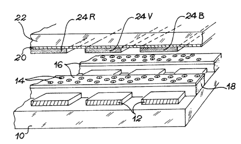
- Fig. 1 diagrammatically shows in
perspective a matrix-type trichromatic screen, such as
could be logically extrapolated from a monochromatic
screen.
, . ~,
13193~0
On a first e.g. glass substrate lO are
provided conductive columns 12 (cathode conductors of
e.g. indium tin oxide) supporting metal, e.g. molybdenum
microtips 14. The columns 12 intersect the perforated
conductive rows 16 (grids) which are e.g. of niobium.
A11 the microtips 14 positioned at an
intersec~ion of a row 16 and a conductive column 12 have
their apex substantially facing a perforation of row 16.
The cathode conductors 12 and grids 16 are separated by
an e.g. silica insulating layer 18 provided with
openings or apertures permitting the passage of the
microtips 14.
A conductive material layer 20 (anode) is
deposited on a second transparent, e.g. glass substrate
22. Parallel bands alternately in phosphors luminescing
in red 24R, in grean 24V and in blue 24B are deposited
on the anode 20 facing the cathode conductors 12. The
bands can be replaced by a mosaic pattern.
In this configuration, it is necessary to
have a triplet of cathode conductors 12 (one facing a
red band 24R, another facing a green band 24V and a
third facing a blue band 24B), in order to bring about
a colour display along a screen column.
Each intersection of a grid 16 and a
cathode conductor 12, in this embodiment, corresponds to
a monochromatic pixel. A ~'colour" pixel is composed by
three monochromatic red, green and blue pixels. The
combination of these three primary colours enables the
viewer's eye to reconstitute a wide coloured spectrum.
~3~ 9390
A screen of this type having N rows and M
columns requires, in the colour mode, N control circuits
for the grids 16, 3M control circuits for the 3M cathode
conductors 12, plus a circuit for the anode 20. ~or
example a colour display screen with 575 rows or lines
and 720 columns (French colour television standard)
comprises 575 control circuits for the grids 16 and 2160
control circuits for the cathode conductors 12.
A microtip monochromatic fluorescent
display screen 14 has 575 control circuits for grids 16
and 720 control circuits for the cathode conductors 12.
Fig. 2 shows a section of the microtip
trichromatic fluorescent screen of fig. 1, as could be
extrapolated by the Expert. As there is only one anode
20, the electrons emitted by the microtips 14 of a pixel
are directed either to the red 24R, green 2~V or blue
24B phosphor. In particular, the lateral emission o~ a
microtip 14 leads electrons intended for a red phosphor
24R, e.g. to a green phosphor 24V. This lateral
emission also exists for monochromatic screens and leads
to a resolution loss. For a trichromatic screen, said
resolution loss is accompanied by a "dilution" of the
colours, which is prejudicial to the viewing quality.
Fig. 3A diagrammatically shows a portion of
a trichromatic screen according to the invention. The
screen is viewed through the diagrammatically
represented second transparent substrate 22. The screen
is subdivided into k zones Zi, i ranging between 1 and
k, three of these Zi-l, Zi and Zi+l being at least
partly visible in fig. 3A. 3N parallel conductive bands
26, N being the number of rows or lines of the screen,
131939~
rest on substrate 22. These bands 26 are e.g. of indium
tin oxide. These conductive bands 26 are grouped and
electrically interconnected in order ~o form three
series of N/k bands each per zone Zi, corresponding to
three anodes Al,i, A2,i and A3,i. Each of the bands 26
is covered by a luminescent material. Fig. 3B
diagrammatically shows a section of the trichromatic
screen according to the invention. This section is
along axis aa' shown in fig. 3A. On the first e.g.
glass substrate 10, the elements are the same and are
arranged in the same way as in the prior art. The
cathode conductors 12 are aligned in accordance with the
screen columns. These cathode conductors 12 support
microtips 14. The grids 16 along the rows of the screen
intersect the cathode conductors 12. The grids 16
(rows) and cathode conductors 12 (columns) are separated
by an insulating layer 18 having apertures permitting
the passage of the microtips.
The second transparent, insulating and e.g.
glass substrate 22 supports the conductive bands 26
aligned on grids 16 and therefore aligned in accordance
with the rows of the screen. These conductive bands 26
are covered with luminescent material. Along the axis
aa', the band 26 shown in fig. 3B is covered with a
material 28, e.g. luminescing in the red.
As can be seen in fig. 4, a first series of
such bands 26 is covered by a material 28 luminescing in
the red, e.g. Eu-doped Y2O2S and forms an anode A1,8 e.~.
for zone Zi, a second series of said bands is covered by
a material 29 luminescing in the green, e.g. CuA1-doped
ZnS and forms an anode A2,i, e.g. for zone Zi; and the
third series of bands 26 is covered by a material 30
131~90
12
luminescing in the blue, e.g. Ag-doped ZnS and forms an
anode A3,i e.g. for zone Zi. The bands 26 of the
different series alternate and are equidistant.
Each triplet formed by an anode of each
series faces a grid 16 (row). The grids 16 rest on a
second substrate 10 (not shown in figs 3A and 4). The
grids 16 intersect cathode conductors 12 (not shown in
figs. 3A and ~). Grids 16 and cathode conductors 12 are
separated by an insulating layer 16 (not shown in figs.
3A and 4). Each intersection of a grid 26 and a cathode
conductor 12 forms a trichromatic pixel.
The grids 16 (along the rows) of the screen
are grouped into N/k families. One zone Zi of the
screen has a single grid 16 of each family. The grids
16 of the different families alternate within a zone Zi
and the grids 16 of the same family are electrically
interconnected.
First exam~le of the process for addressing a microtip
fluorescent trichromatic screen according to the
invention ffiqs. 5 and 6)
This process consists of dividing the
display time of a frame T into three:
a subframe time T1 corresponds to the
display of a first frame, e.g. red, of the screen,
a subframe time T2 corresponds to the
display of a second frame, e.g. green, of the screen,
a subframe time T3 corresponds to the
display of a third frame, e.g. blue, of the screen,
Tl, T2, T3 being connected by the relation
Tl + T2 + T3 = T.
~ls~a
The red, green and blue frames of the
picture are successively displayed.
As can be seen in fig. 5 within the
subframe time Tl (T2, T3 respectively), during which i~
displayed the red frame (green, blue respectively~ of
the screen, the k anodes of the zones Zl, ..., Zk
correspond to red (respectively green, blue), designated
Al,i (respectively A2,i A3,i) are successively
addressed. This addressing consists of raising each
anode Al,i (respectively A2,i, A3,i) successively to a
potential VAlmax (respectively VA2max, VA3max) during a
time tl (respectively t2, t3). This potential VAlmax
(respectively VA2max, VA3max) is adequate for attracting
the electrons optionally emitted by the microtips with
an energy higher than the threshold cathodoluminescence
energy of the material 28 (respectively 29, 30)
luminescing in the red (or green or blue). Outside the
addressing time tl, the anodes Al,i (respectively A2,i
and A3,i) are raised to a potential VAlmin (respectively
VA2min, VA3min), such that the electrons emitted by the
microtips are repelled and eliminated by means of a grid
16, or have an energy below the threshold
cathodoluminescence energy of the luminescent material
corresponding thereto and are also eliminated.
The subframe time Tl (respectively T2, T3)
is iinked with the addressing time tl (respectively t2,
t3) of an anode Al,i (respectively A2,i A3,i) by the
relation: Tl = ktl (respectively T2=kt2, T3=kt3).
The frame times Tl, T2 and T3 and the
values of the addressing potentials of the anodes are
experimentally adjusted as a function of the luminescent
,. ,
1 319~
14
materials 28, 29 and 30, so as to obtain a pure white
when all the scresn is addressed.
Fig. 6 diagrammatically shows the timing
diagrams relating to the first process for addressing a
pixel of a trichromatic screen according to the
invention.
The display of a trichromatic frame of the
screen takes place in a frame time T subdivided into
three subframe times Tl, T2 and T3 corresponding to the
respective display of a red, green and blue frame.
Fig. 6 only shows the addressing of the
anodes Al,i, A2,i and A3,i of zone Zi. These addressing
operations take place during respective addressing
periods tl, t2 and t3, the first being within the red
frame, the second within the green frame and the third
within thP blue frame.
The grids 16 are addressed by families.
The pixels involved in each addressing of a family of
rows are those corresponding to the superimposing of a
row of the addressed family with the selected anode.
The families of rows Gj, j ranging between
1 and N/k, are raised to a potential VGj. VGj assumes
a value VGmax for the row selection times ~1,
periodically at period tl, for the entire frame time Tl,
then VGj assumes the value VGmax for the row selection
time ~2, periodically at period t2, throughout the frame
time T2 and then VGj assumes the value VGmax for a row
selection time ~3, periodically at period t3, for the
entire frame time T3. Outside the row selection times,
131~39~
VGj assumes the value VGmin permitting no electron
emission by microtips 14.
The addressing times tl, t2 and t3 are
linked with the row selection time ~ 2 and ~3 by the
relations: tl/~l = t2/~2 = t3/~3 = N/k.
The "illumination" of the pixels positioned
on the row of family Gj facing the anodes of zone Zi is
controlled by the potential applied to the cathode
conductors 12.
The three timing diagrams Cl, C2 and C3 of
fig. 6 represent the control signals VCl of the cathode
conductor 12 of number 1 in the matrix making it
possible to "illuminate" the pixel corresponding to the
intersection of the row of family Gj in zon~ Zi with the
cathode conductor 12 of number 1, said pixel being ijl.
Timinq diaqram Cl: pixel ijl "illuminated" in red.
To illuminate the pixel ijl in red, the
control potential VCl of cathode conductor 12 of number
1 assumes a value VCmin during the selection time ~1 of
the row of family Gj in zone Zi. The potential
difference VGmax-VCmin permits the emission of electrons
by microtips 14. Pixel ijl is extinguished in the two
other colours, because the potential VCl then assumes
the value VCmax not permitting the emission of electrons
by the microtips 14 during selection times ~2 and ~3 of
the row of family Gj.
Timina diaaram C2: Pixel ijl "illuminated" in the three
primary colours red, green and blue= pixel ijl "white".
"' .,
~3~9~
16
For each selection of the row corresponding
to pixel ijl, the potential VCl assumes the value VCmin.
Pixel ijl successively assumes the colours red, green
and blue, the white colour being restored by the
psrsistence of vision of a viewer's eye.
T.iminq diagram C3: Pixel ijl "extinguished", pixel ijl
"black".
For each selection of the row corresponding
to pixel ijl, potential VCl is maintained at the value
VCmax, no colour being "illuminated".
Example of numerical data corresponding to
the first process for addressing a trichromatic screen
according to the invention:
N: number of rows 500
k: number of zones 20
20 T: frame time 20 ms
Tl: red frame time 5 ms
T2: green frame time 5 ms
T3: blue frame time 10 ms
tl: addressing time of a red anode in a zone
5 ms/20 = 0.25ms
t2: addressing time of a green anode in a zone
5 ms/20 = 0.25 ms
t3: addressing time of a blue anode in a zone
10 ms/20 = 0.5 ms
30 ~1: selection time of a family of rows during the
addressing of a red anode 0.25 ms/25 = 10 ~s
~2: selection time of a family of rows during the
addressing of a green anode 10 ~s
13~3~
17
~3: selection time of a family of rows during the
addressing of a blue anode 20 ~s
VAl: addressing potential of anodes Al,i:
VAlmin = 40 V, VAlmax = 100 V
VA2: addressing potential of anodes A2,i:
VA2min = 40 V, VA2max = 100 V
VA3: Addressing potential of anodes A3,i:
VA/min = 40 V, VA3max = 150 V
~Gj: addressing potential of a family of raws:
VGmin = -40 V, VGmax = 40 V
VCl: control potential of column 1:
VCmin = -40 V, VCmax = 0 ~.
Second example of process for addressinq a microtiP
fluorescent trichromatic screen accordinq to the
invention (fi~s 7 and 8)
This process consists of the row by row
addressing of the three primary colours for each pixel.
Fig. 7 shows the addressing sequences of
anodes Al,i, ....... Al,k of zones Zl to Zk respectively.
Anodes Al,i, A2,i and A3,i, i ranging between 1 and k,
are successively addressed. The display frame time T is
subdivided into zone times tZ during which all the rows
of one zone are addressed. The frame time T and the
zone time tZ are linked by the relation T = k.tZ.
Each anode Al,i (respectively A2,i, A3,i)
is addressed for an addressing time tl (respectively t2,
t3), for the zone time tZ and at the period of a frame
time T.
, . .
l3ls3~a
During the zone time tZ, an anode Al,i
(respectively A2,i A3,i) is periodically raised during
an addressing time tl (respectively t2, t3) to a
potential VAlmax (respectively VA2max, VA3max) adequate
for attracting the electrons emitted by the microtips 14
with an energy exceeding the threshold
cathodoluminescence energy of the material 28
(respectively 29, 30). The period is in this case t the
selection time of a row in a zone. Thus the zone time
is linked with the row selection time t by the relation
tZ = N/k.t.
The addressing times tl, t2 and t3 of the
anodes Al,i, A2,i and A3,i respectively are linked with
the row selection times t by the relation tl + t2 + t3
= t.
Outside the addressing times, the anodes
Al,i (respectively A2,i, A3,i) are raised to a potential
VAlmin (respectively VA2min, VA3min) such that the
electrons emitted by the microtips 14 are rejected
towards the grids 16 and eliminated or have an energy
below the threshold cathodoluminescence energy of the
luminescent material corresponding thereto and are also
eliminated.
Fig. 8 diagrammatically shows the timing
diagrams relating to the second process for addressing
a pixel of a trichromatic screen according to the
invention.
The displaying of a trichromatic frame of
the screen takes place in a frame time T, which is
13~3~
19
subdivided into zone times tZ. In a zone time tZ, all
the rows of a zone are successively addressed.
The timing diagrams of fig. 8 represent the
addressing of the pixel ijl. The families of rows Gj,
j ranging between 1 and N/k, are successively raised to
a potential VGmax. VGj assumes a value VGmax during th~
row selection time t at period tZ. During the ro~
selection time t, the three anodes Al,i A2,i A3,i of
zone Zi are consequently successively addressed during
the re~pective addressing times tl, t2 and t3.
The "illumination" of the pixels positioned
on the row of family Gj facing the anodes of zone Zi is
controlled by the potential applied to the cathode
conductors 12.
The three timing diagrams C4, C5 and C6 of
fig. 8 show the control signals VCl of the cathode
conductor 12 of number 1 making it possible to
"illuminate" the pixel ijl.
Timing diaqram C4: Pixel ijl "illuminated" in red.
In order to "illuminate" the selected pixel
ijl in red, the control potential VCl of the cathode
conductor 12 of number 1 assumes the value VCmin during
the addressing time tl of anode Al,i. VCl is kept at
value VCmax for the addressing times t2 and t3 of anodes
A2,i and A3,i (corresponding to green and blue~.
Timina dia~ram C5: Pixel ijl "illuminated" in the three
primary colours red, green and blue = pixel ijl "white".
1 3 ~
The potential VCl is maintained at the
value VCmin for the entire row selection time, which
permits the emission of the electrons by the microtips
14 during each addressing time tl, t2 and t3 of anodes
Al,i, A2,i and A3,i.
Timinq diaqram C6: Pixel ijl "extinguished", pixel ijl
"black".
On this occasion the potential VCl is
maintained during the row selection time at value VCmax
not permitting the emission of electrons, so that the
pixel ijl is "black".
Example of numerical data corresponding to
the second process for addressing a trichromatic screen
according to the invention:
N number of rows 500
20 k: number of zones 20
T: frame time 20 ms
tZ: zone time 1 ms
t: row selection time 1 ms/25 = 40 ~s
tl: addressing time of an anode Al,i = 10 ~s
25 t2: addressing time of an anode A2,i = 10 ~s
t3: addressing time of an anode A3,i = 20 ~s
VAl: addressing potential of anodes Al,i:
VAlmin = 40 V, Valmax = 100 V
VA2: addressing potential of anodes A~,i:
VA2min = 40 V, VA2max = 100 V
VA3: addressing potential of anodes A3,i:
VA3min = 40 V, VA3max = 150 V
VGj: addressing potential of a family of rows
VGmin = -40 V, VGmax = +40 V
13~39~
VCl: control potential of column 1:
VCmin - -40 V, VCmax = 0 V.
A microtip fluorescent trichromatic screen
according to the invention with 575 rows and 720 columns
(French television standard) can operate wikh 23
families of rows, 25 red anodes, 25 green anodes, 25
blue anodes and 720 cathode conductors, i.e. 818 outputs
to be controlled each by a different electric circuit.
This is to be compared with a screen such as could be
extrapolated by the Expert (figs. 1 and 2), i.e~ 575
grids and 3x720 cathode conductors, i.e. 2735 ou~puts to
be controlled, each by a different electric circuit.
At a given instant, all the electrons
emitted are either repelled to a grid or have an energy
below the threshold cathodoluminescence energy of the
luminescent material, or are attracted by a luminescent
phosphor in a given primary colour. The lateral
electron emission of the microtips 14 consequently
produces no diaphony phenomenon characterized by a
dilution of the colours.
The invention can also apply to microtip
monochromatic fluorescent screens. The screen is
subdivided into k zones Zi~ i ranging between l and k
and the N rows are grouped into N/k families. The rows
(grids 16) of the samefamily are electrically
interconnected. Each zone Zi only comprises a single
row of each family. The rows 16 of each family succeed
one another within a zone ~i.
Fig. 9 diagrammatically shows part of a
monochromatic screen according to the invention. The
-. .
13193~0
screen is seen through the second, diagrammatically
shown, transparent substrate 22. on the latter are
located N conductive bands 26, which are electrically
connected by groups of N/k bands 26 to form k anodes Ai:
one anode Ai per zone Zi. Anodes ~i are covered by a
luminescent material 31, e.g. ZnS.
In the same way as for a trichromatic
screen, the bands 26 face grids 16 (rows). The grids 16
intersect the cathode conductors 12 (not shown in fig.
9). Grids 16 and cathode conductors 20 are separated by
an insulating layer 16 (not shown in fig. 9). Each
intersection of a row (grid 16) and a column (cathode
conductor 12) forms a pixel.
The section of such a monochromatic screen
along an axis of a conductive band 26 is identical to
the section of a trichromatic screen shown in fig. 3B,
the luminescent material 31 replacing material 28. A
single luminescent material 31 is deposited on each
conductive band 26.
Example of a process for addressinq a monochromatic
screen accordin~ to the invention (fig. 10)
The timin~ diagrams relating to this
addressing process are diagrammatically shown in fig.
10. They relate to the "illumination" of pixel ijl
located at the intersection of the row of family Gj in
zone Zi with the cathode conductor (column) of number l
in the matrix.
A frame of a picture is displayed for a
frame time T. The anodes Ai,i ranging between 1 and k,
13193~
are successively addressed during an addressing time tZ.
The addressing of an anode Ai consists of ràising the
potential VAi supplied to said anode to the value VAmax
during the addressing time tZ. The potential VAmax is
such that it attracts the electrons optionally emitted
by the microtips 14 with an energy exceeding the
threshold cathodoluminescence energy of the material 31.
Outside the addressing time tZ, the potential Vhi is
maintained at a value V~min such that the electrons
emitted by the microtips are repelled towards a grid 16
or have an energy below the threshold
cathodoluminescence energy of the luminescent material.
A family of rows Gi is periodically
addressed during a row selection time t. The potential
VGj supplied to the family of rows Gj then assumes the
value VGmax during t at period tZ. The different
families of rows are successively addressed during the
period tZ. Potential VGmax permits the emission of
electrons. Outside the row selection time, VGj assumes
the value VGmin not permitting the emission of
electrons.
During the addressing time t of the row of
the family Gj in zone Zi, potential VC1 applied to the
cathode conductor of number 1 assumes a value VCmin for
the "illumination" of pixel ijl and a value VCmax if the
pixel must remain "extinguished". Thus, VCmin is such
that the potential difference VGmax-VCmin is adequate
for tearing away electrons at the microtips, whereas
VGmax-VCmax is not.
Examples of numerical date relating to this
addressing process:
,. ~
~31 93~0
24
N: number of rows 500
k: number of zones 20
T: frame time 20 ms
tZ: addressing time of an anode Ai = 1 ms
5 t: row selection time 40 ~s
VAi: addressing potential of anode ~i:
VAmax = 100 V, VAmin = 40 V
VGj: addressing potential of a family of rows Gj:
VGmax = 40 V, VGmin = -40 V
lO VCl: control potential of column 1:
VCmax = 0 V, VCmin = -40 V.
This type of monochromatic screen only
requires N/k addressing circuits for families of rows,
k addressing circuits for the anodes and obviously M
control circuits for the cathode conductors (for a
screen with M columns). However, a microtip
monochromatic fluorescent screen according to the prior
art requires N addressing circuits for the rows and M
addressing circuits for the column, so that the gains
are significant.
For producing a family of rows which are
electrically connected to one another and for producing
an anode (formed by electrically interconnected
conductive bands 26), it is e.g. possible to etch in a
conductive material parallel bands of appropriate
dimensions. The different bands of each family of rows
or each anode are electrically interconnected via an
anisotropic conductive film electrically contacted with
a metal ribbon or tape. This film is only conductive at
certain crushing points located on the bands to be
connected. The conductive crushing points are
interconnected by the metal ribbon.