Note: Descriptions are shown in the official language in which they were submitted.
- 1 - 41PR06679
MOLDED CASE CIRCUIT BREAKER
ACTUATOR-ACCESSORY MODULE
BACKGROUND OF THE INVENTION
The trend in the circuit protection industr~
is currently toward complete circuit protection which
is accomplished by the addition of supplemental
protection apparatus to standard overcurrent
protective devices, such as molded case circuit
breakers. U.S. Patent No. 4,622,444, issued November
11, 1986 to Kandatsu et al, entitled "Circuit Breaker
Housing And Attachment Box" describes an accessory
that can be field-installed within a circuit breaker
without interfering with the integrity of the circuit
breaker internal components. This is accomplished by
mounting the accessories within a recess formed in the
circuit breaker enclosure cover.
An electronic trip actuator which is mounted
within the circuit breaker enclosure is described
within U.S. Patent 4,679,019, issued July 7, 1987 to
Todaro et al, entitled "Trip Actuator for Molded Case
Circuit Breakers". The circuit breaker actuator
responds to trip signals generated by an electronic
2 - 41PR0667g
trip unit completely contained within a semiconductor
chip such as that described within U.S. Patent
4,589,052, issued May 13, 1986 to Dougherty. The
devQlopment of a combined trip actua~or for both
overcurrent protection as well as accessory function
is found within U.s. Patent ~,700,161, issued October
13, 1987 to Todaro Pt al, entitled ~Combined Trip Unit
And Accessory Module for Electronic Trip Circuit
Breakers".
A shunt trip accessory unit allows the
circuit breaker operating mechanism to be articulated
from a remote location to separate the circuit breaker
contacts, usually to perform a tripping ~unction for
electrical system control and protection. one such
shunt trip accessory unit is described within U.S.
Patent 4,786,885, issued November 22, 1988 to Morris
et al, entitled "Molded Case Circuit Breaker Shunt
Trip Unit"~ An auxiliary switch accessory unit allows
an operator to determine the "ON" or "OFF" conditions
of a molded case circuit breaker contacts at a remote
location by means of an audible alarm or visible
display. One such auxiliary switch unit is described
within Canadian Application Serial No. 584,739, filed
Dec~ 1, 1988, Yu et al, entitled "Molded Case
Circuit Breaker Auxiliary Switch Unit".
A more recent example of a combined
overcurrent trip actuator and multiple accessory unit
is described within U.S. Patent No. 4,788,621, issued
November 29, 1988 to Russell et al, entitled "Molded
Case Circuit Breaker Multiple Accessory Unit" which
combined overcurrent trip actuator and multiple
accessory unit requires a separate mounting recess
within the circuit breaker cover to house the printed
wire board that carries the accessory control
circuit. Canadian Application Serial No. 590,580,
~31~
- 3 - 41PR06579
filed February 9, 1989, Castonguay et al, entitled
"Molded Case Circuit Breaker Actuator-Accessory
unit" describes one such combined overcurrent trip
actuator and multiple accessory unit wherein the
printed wire board and actuator-accessory unit are
both contained within the same mounting recess
within the circuit breaker cover. Canadian Patent
No. 1,304,112, issued June 23, 1992, Russell,
describes an actuator- accessory module wherein the
electromagnetic actuator and electronic control
circuits are self-contained within a single unitary
module. Canadian Patent No. 1,305,990~ issued
August 4, 1992, Russell, entitled "Molded Case
Circuit Breaker Actuator-~ccessory ~odule" describes
an arrangement whereby a separate actuator-accessory
module is selected for different combinations of
accessory functions.
SUMMARY OF THE INVENTION
An integrated protection module which
includes overcurrent protection along with auxiliary
accessory function within a common enclosure contains
an accessory cover for access to the selected
accessory modules to allow field installation of the
accessory modules within an integrated protection
unit. One combined actuator-accessory module provides
overcurrent protection along with shunt trip function
and ground fault protection. The electromagnetic
actuator includes a first coil for overcurrent
operation and a second coil for shunt trip operation.
The overcurrent electronic control is provided by the
electronic trip circuit contained within the circuit
breaker portion of the integrated protection unit or
by means of a thermal-magnetic trip unit whereas the
shunt trip control and ground ~ault protection is
provided by an electronic circuit contained within the
- 4 - 41YR06679
accessory module.
BRIEF DESCRIPTION OF THE DRAWINGS
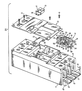
Figure l i~ a top perspective view of an
integrated molded case circuit breaker containing an
overcurrent, shunt trip and ground fault
actuator-accessory module according to the invention;
Figure 2 is an exploded top perspective view
of the integrated circuit breaker of Figure 1 prior to
assembly of the overcurrent, shunt trip and ground
fault actuator-accessory module according to the
invention;
Figure 3 is a plan view of the integrated
molded case circuit breaker with part of the cover
removed to show the interaction between the circuit
breaker operating mechanism and the combined
overcurrent, shunt trip and ground fault
actuator-accessory module of Figure 2; and
Figure 4 is a circuit diagram of the shunt
trip and ground fault electrical circuit contained
within the printed wire board for the overcurrent,
shunt trip and ground fault actuator-accessory module
of Figure 2.
DESCRIPTION OF THE PREFERRED EMBODIMENT
An integrated circuit breaker 10 consisting
of a molded plastic case ll with a molded plastic
cover 12 is shown in Figure l with the accessory cover
13 attached to the circuit breaker cover by means of
screws 14. The case includes a wiring slot 18 formed
therein for allowing external connection with a remote
switch by means of conductors 34. The circuit breaker
operating handle l9 extends up from an access slot 20
formed in the cover escutcheon 9. A rating plug 15
such as described in U.S. Patent 4,728,gl4, issued
March l, 1988 to Morris et al, entitled "Rating Plug
enclosure for Molded Case Circuit Breakers". A pair
~ 3
~ . tj ',1.~1~ æl
- 5 - 41PR06679
of accessory doors 16, 17 are formed in the accessory
cover for providing access to the overcurrent and
shunt trip actuator and accessory module 31, hereafter
"actuator-accessory module" contained within the
recess 40, shown in Figure 2. Still referring to
Figure 2, the rating plug 15 is fitted within a recess
23 formed in the accessory cover 13 and the accessory
cover is fastened to the circuit breaker cover by
means of screws 14, thru-holes 24 and threaded
openings 25. Access to the rating plug interior for
calibration purposes is made by means of the rating
plug access hole 21.
The trip unit for the integrated circuit
breaker lo is contained within a printed wire board 27
15 which is positioned in the trip unit recess 26. The
rating plug 15 when inserted within the rating plug
recess interconnects with the printed wire board by
means of pins 28 upstanding from the printed wire
board and sockets 29 formed on the bottom of the
20 rating plug. The trip unit in turn electrically
connects with the current transformers 47, 48 (Figure
3) by means described within U.S. Patent 4,652 ~ 975,
issued March 24, 1987 to Scott, entitled "Mounting
Arrangement for Circuit Breaker Current Sensing
Transformers". When the trip unit printed wire board
has been assembled within its recess, the
actuator-accessory module 31 is then installed within
recess 40. In some applications the printed wire
board and rating plug are omitted and a
thermal-magnetic trip unit is used for overcurrent
protection while the accessory functions are
separately provided by the actuator-accessory module
per se. One example of one such thermal-magnetic
trip unit is found in U.S. Patent 4,706,054, issued
November 10, 1987 to Hampton et al. The
~ 3 ~
- 6 - 41PRO6679
actuator-accessory modul~ includes a housing 32 within
which the dual actuator~accessory coil 35 is enclosed
and which further contains a plunger 36 and a plunger
spring 41 which projects the plunger in a forward trip
position when the dual actuator-accessory coil 35
becomes energized. The actuator-accessory module is
similar to the actuator-accessory unit described
within aforementioned Canadian Application Serial No.
590,580 o~ Castonguay et al wherein a trip actuator
latch 37 is pivotally at~ached to the housing 32. A
hook 38 formed at one end of the trip actuator latch
cooperates with the circuit breaker operating
mechanism shown in aforementioned U.S. Patent
4,700,161 in the manner to be described below in
greater detail. The operation of the
actuator-accessory module is similar to that described
within U.S. Patent 4,641,117, issued February 3, 1987
to Willard and the aforementioned U.S. Patent
4,679,019. The dual actuator-accessory coil 35
differs from that described within some of the
referenced Patents by including a separate flux shift
coil 22 for overcurrent trip operation and a separate
shunt trip coil 60 for remote shunt trip operation. A
permanent magnet 59 is provided at the end of both
coils to hold the plunger 36 against the bias exerted
on the plunger by the charged plunger spring 41. A
similar combined accessory and trip actuator unit is
described within the aforementioned U.S. patent
4,641,117, entitled "Combined Accessory and Trip
Actuator Unit for Electronic Circuit Breakers". The
actuator-accessory module includes a printed wire
board 33 which contains the components required for
operating the shunt trip coil 60 and is connected with
the shunt trip coil by means of a pair of wire
conductors 67, 68. A pair of wire conductors 34
~3~g~ f~ ~3
- 7 - 41PR06679
connect the actuator-accessory module with an external
voltage source and switch for shunt trip operation.
The flux shift coil 22 connects with the trip unit 27
by means of a pair of wire conductors 69 attached to
the coil and by means of edge connectors 61 arranged
within the housing for receiving a pair of pins 30
upstanding on the trip unit 27.
The actuator-accessory module 31 is depicted
in Figure 3 within the recess 40 in the integrated
circuit breaker 10 with part of the actuator--accessory
module printed wire board 33, actuator-accessory
module housing 32 and accessory cover 13 removed to
show the interaction between the actuator-accessory
module 31 and the mechanical actuator 50 which sits in
the integrated circuit breaker case 11. The
integrated circuit breaker operating mechanism shown
generally at 53 includes an operating cradle 54 having
a hook 55 formed at one end thereof which is retained
by means of a primary latch 56. The secondary latch
assembly 57 prevents the primary latch from releasing
the operating cradle until the secondary latch is
displaced. A tab 58 extending from the secondary
latch is contacted by the operation of the mechanical
actuator 50 to displace the secondary latch and
thereby articulate the circuit breaker operating
mechanism in response to a trip command in the
ollowing manner. Electric current flow is sensed by
the current transformers 47, 48 which are located
ahead of load lugs 51, 52 and is acted upon by the
trip unit 27 described earlier with reference to
Figure 2. The operating lever 46 sits within the case
11 and connects with the latch support arm 44 in the
actuator-accessory module recess 40 by means of a
connecting arm 45. The latch pin ~3 is retained by
the trip actuator latch 37 which is in turn controlled
r~
~ 8 ~ 41PR06679
by the position of the trip actuator arm 39 which
extends through a side wall 42 of the
actuator-accessory module housing 32. The trip
actuator arm 39 interfaces with the plunger 36 in the
following manner. When the circuit current exceeds a
predetermined value, current is applied to the flux
shift coil 22 thereby allowing the plunger 36 to be
propelled by the urgence of the plunger spring (Figure
2) to thereby rotate the trip actuator latch 37 in the
clockwise direction to release the trip actuator latch
37 from the latch pin 43.
The shunt trip function is provided by means
of the accessory circuit 90 which includes the input
circuit 62, shunt trip circuit 82 and ground fault
circuit 83 seen by now referring to both Figure 2 and
Figure 4. It is noted that an auxiliary switch, such
as described within the referenced actuator-accessory
Patents is no longer required to interrupt the
external voltage signal applied to the shunt trip coil
60. In operation, the remote shunt trip signal
voltage is applied to wire conductors 34 and terminals
Tl, T2 connected to the shunt trip circuit 82 through
a bridge rectifier 63 consisting of diodes Dg-Dl2
and current limiting resistor R14 via conductors 86,
87. External power is supplied to the accessory
circuit over external wire conductors 80 and input
terminals T5, T6. Transient voltage protection is
provided to the input circuit by the combination of
the series resistor Rl and zener diode Zl which
are connected across the input terminals. Resistor
R2 is a current limiting resistor connected in
series with one of the inputs to the diode bridge
rectifier 49 consisting of diodes Dl-D4. The
output of the bridge rectifier connects respectively
with the positive and negative rails 70, 71. A
,~ ~c~ r~
- 9 - 41PR06679
charging circuit 64 consisting essentially of a
storage capacitor ~1 connects across the positive
and negative rails through an FET and resistors R3,
R4. The function of the charging circuit is to
provide ~irst and second charging rates to the storage
capacitor C1O The first charging rate charges the
capacitor in less than 1o milliseconds and is provided
by the charging circuit consisting of the FET,
resistors R3, R5, R6, a signal diode D5 and a
zener diode Z2 When voltage is applied over
conductors 80 to terminals T5, T6 base drive is
applied to transistor Q5 through resistor R13
turning on Q5. This clamps the gate of the FET to
less than 2 volts and disables the fast charge circuit
to the storage capacitor C1 through the FET. To
institute a shunt trip operation, a voltage is applied
to terminals T1, T2 over conductor 34 through the
bridge rectifier 63 including diodes Dg-D12 and
current limiting resistor R14 onto conductors 86,
87. This executes the photo diode D16 within the
opto-isolator 84 and turns on the photo transistor
Q6 causing the base drive to ~5 to become diverted
to the ground rail 71 through diodes D7, D15
turning off Q5. The voltage on the gate of the FET
exceeds 2 volts thereby charging C1, which becomes
completely charged in a period of time less than 10
milliseconds. The voltage across Cl is applied
across resistor R7, silicon switch Q1 and zener
diode Z3 within the switching circuit 65. When the
silicon switch trigger voltage is exceeded, the switch
becomes conductive thereby discharging capacitor C
through the shunt trip coil 60 which is connected
between the charging circuit 64 and the electronic
switch 74 by means of conductors 67, 68 and terminals
T3, T4 described earlier. The shunt trip coil
'.L ~, ~3
- 10 - 41PR06679
immediately responds by providing an electromagnetic
field in opposition to the permanent magnet 59 within
the actuator-accessory module 31 of Figure 2 and
allows the plunger 36 to interact with the trip
actuator latch 37 and thereby articulate the circuit
breaker operating mechanism 53 shown in Figure 3 and
described earlier. The fly-back diode D6 is
connected across the shunt trip coil to prevent the
occurrence of a transient voltage when the circuit
turns off. Once the circuit breaker operating
mechanism has responded, and the external voltage
signal remains applied to the terminals T1, T2, some
means is usually required to insure that the circuit
breaker operating mechanism cannot be reset until the
remote switch is deactivated. In the prior art
arrangement, described earlier, an auxiliary switch
interacted with the circuit breaker operating
mechanism to interrupt the current applied to the
shunt trip coil and to prevent the coil from becoming
overheated. The auxiliary switch mechanically
interacted with the circuit breaker operating
mechanism to insure that the circuit breaker operating
mechanism could not be reset without first resetting
the auxiliary switch. Since the actuator-accessory
module of the instant invention does not include nor
require an auxiliary switch, the circuits, per se,
insure that the circuit breaker operating mechanism
cannot be reset manually while a voltage signal
remains impressed across the terminals T1, T2. This
is provided by the second capacitor charging circuit
through resistor R4 which by-passes the FET in its
"OFF" states. The charging current applied to the
storage capacitor fully charges the storage capacitor
within one to two seconds. The silicon switch
responds in the manner described earlier to
~ 3 ~
~ 41P~06679
continuously provide a current pulse to the shunt trip
coil 60 every seconcl or so to insure that the circuit
breaker operating mechanism remains in a "TRIPPED"
condition while the terminals ~1, T2 remain
energized. The switching function is provided by
means of an electronic switch 74 consisting of the
silicon switch Ql~ zener diode Z3, resistors R7,
R8 and transistor switches Q2, Q3 The
electronic switch operates in the manner described in
the aforementioned Canadian Patent Number
1,304,112. The repeated ON and OFF operation of the
electronic switch insures that the required trip
current is applied to the shunt tr.ip coil 60 without
causing the coil to become overheated. Once the
electronic switch is turned off, the storage capacitor
begins to recharge. With the silicon switch Q1
conductive, current flows through resistor R7 and
the emitter-base junction o~ the transistor switch
Q2 causing Q2 to become conductive. Current then
flows through resistor R8 and the emitter-base
junction of transistor switch Q3 causing Q3 to
become conductive. With Q3 conductive, current is
shunted away from the silicon switch Q1 turning off
the silicon switch and drawing more current through
transistor switch Q2 which thereby provides a
regenerative latching action that insures that the
electronic switch remains on until the discharge
current from the storage capacitor decreases to a
predetermined value set by the resistor R8. When
the trip current through the shunt trip coil drops
below the predetermined value, the electronic switch
becomes non-conductive and thereby allows the storage
capacitor to charge to a voltage su~ficient to exceed
the trigger voltage to the silicon switch Ql causing
the ON-OFF cycle to repeat itself. The timing circuit
~ ~ ~,.r~
- 12 - ~lPR06679
66 for controlliny the ~ON~ - "OFF" states of the FET
connects with the positive rail 70 through resistor
Rg and operates in the following manner. When
terminals T5, T6 are energized, the timing capacitor
C2 charges to a voltage determined by zener diode
Zs, resistor R12 and the capacitor C2. Resistor
Rll, connected across the base-emitter junction of
transistor switch Q4, insures that Q4 remains
non-conductive. When the timing capacitor C2
exceeds the voltage of Z4, current flows through
resistors R9, R1o, zener diode Z4 and resistor
Rll to turn on Q~. With Q4 conductive, the gate
terminal of the FET is clamped to the negative rail 71
through resistor R6 turning off the FET. This, in
turn, initiates the second charging circuit through
resistor R4 as described earlier.
Still referring to Figures 2 and 4, the
ground fault trip function is provided in the
following manner. The three-phase currents through
line terminal buses 75-77 is sensed within a zero
sequence current transformer 7~ shown in phantom in
Figure 2 which connects with the actuator-accessory
printed wire board 33 over wire conductors 81.
Althouqh the zero sequence current transformer is
described as arranged around the line terminal buses,
this is by way of example only. It is to be clearly
understood that the zero sequence current transformer
can be arranged around the load terminal buses, if
desired. The zero sequence current transformer
operates in the manner described within UOS. Patent
4,121,269, issued October 17, 1978 to Hobson, Jr.,
entitled "Ground Fault Signal Circuit for Circuit
Breaker Trip Unit" to sense the occurrence of a ground
fault current appearing within the protected circuit
to which the terminal buses are connected. When a
- 13 - 41PR06679
ground fault signal is accordingly applied to
terminals T7, T8 over the wire conductors 81, the
signal appearing on conductors 88, 89 is clamped to
approximately one volt by means of the back-to-back
diodes D13, D14 and burden resistor R20. An
averaging circuit including resistor R18, Rlg and
capacitor C4 produces an average ground fault
voltage value onto the negative input terminal to the
comparator 85. Operating voltage to the comparator is
applied to pin 1 which connects with the positive
rails 70 through resistor R15 and through pin 2
which connects with the negative rail. Power to the
comparator is filtered and regulated by the zener
diode Z6 and capacitor C3. The reference voltage
is supplied to the positive input terminal to the
comparator by the midpoin~ of the voltage divider
consisting of resistors R16, R17. When the ground
fault signal exceeds the reference voltage an output
signal from the comparator is applied through diode
D8 to the base of Q5 thereby clamping the base of
Q5 to a low level and causing Q5 to become
non-conducting. This will activate the shunt trip
coil 60 in the manner described earlier and thereby
institute a circuit interruption.
It has thus been shown that an
actuator-accessory module containing a flux shift coil
for direct operations by means of the circuit breaker
trip unit for overcurrent protection and a shunt trip
coil connected with a self-contained shunt trip and
ground fault circuit for shunt trip operations via a
remote voltage source switch and upon the occurrence
of a ground fault condition can be provided within a
single actuator-accessory module. The shunt trip
circuit initiates a continuous series of trip current
pulses to the shunt trip coil, without overheating to
~ 3 ~ 3 l~.3
- 14 - 41PR0667g
insure that the circuit breaker operating mechanism
remains tripped as long as an external signal voltage
is applied to the shunt trip circuit within the
actuator-accessory module.