Note: Descriptions are shown in the official language in which they were submitted.
- 1 - RCA 81,636
PIXEL INT~RP~LATION CIRCUITRY
AS FOR A VIDEO SIGNAL PROCFSSOR
FIELD OF THE INVENTION
The present invention relates to pipelined
circuitry which interpolates pixel data in two dimensions.
BRIEF DESCRIPTIO~ OF THE_DR~WINGS
FIGURES lA, lB and lC are diagrams showing the data
formats of records produced by three data compression
methods.
FIGURE 2 is a block diagram of video signal
processing circuitry which includes an embodiment of the
present invention.
FIGURE 3A is a block diagram showing circuitry
suitable for use as the microcode RAM and sequencing
circuitry of the video signal processing circuitry shown in
FIGURE 2.
FIGURE 3B is a timing diagram showing signal
amplitudes as a function of time for several signals that
are useful in explaining the operation of the circuitry
shown in FIGURE 3A.
FIGURE 3C is a diagram showing the data format of a
microcode control word for the microcode RAM and sequencer
used in the circuitry shown in FIGURE 2.
FIGURE 4A is a block diagram of the arithmetic and
logic unit used with the embodiment of the invention shown
in FIGURE 2.
FIGURE 4B is a partial block diagram of the
arithmetic and logic circuitry shown in FIGURE 4A.
FIGURE 5 is a block diagram of the data path
circuitry used with the embodiment of the invention shown in
FIGURE 2.
FIGURE 6 is a block diagram of the data RAM
circuitry used with the embodiment of the invention shown in
FIGURE 2.
FIGURES 7A, 7B, 7C, 7D and 7E are timing diagrams
that are useful for explaining the operation of the data RAM
circuitry shown in FIGURE 6.
- 2 - RCA 81,636
FIGURE 8A is a block diagram of the pixel
interpolator which embodies the present invention.
FIGURE 8B is a block diagram of the multiplier used
with the pixel interpolator shown in FIGURE 8A.
FIGURES 9A, 9s, 9C, 9D, 9E and 9F are diagrams that
are useful to explain the operation of the pixel
interpolator shown in EIGURE 8A.
FIGURE lOA is a block diagram of a statistical
decoder suitable for use in the video signal processing
circuitry shown in FIGURE 2.
FIGURE 10B iS a timing diagram that is useful for
understanding the operation of the circuitry shown in FIGURE
lOA.
FIGURE llA is a block diagram of input FIFO
circuitry suitable for use in the video signal processing
circuitry shown in FIGURE 2.
FIGURE llB is a timing diagram that is useful for
understandin~ the operation of the circuitry shown in FIG~lRE llA.
FIGURE 12A is a block diagram of output FIFO
circuitry suitable for use in the video signal processing
circuitry shown in FIGURE 2.
FIGUEæ 12B is a t~ning diagram th~t is useful for understanding
the operation of the circuitry shown in FIGt7RE 12A~
FIGURE 13A and 13B are a block diagram of the VRAM
corltrol unit used with the embodiment of the invention shown
in FIGURE 2.
FIGURE 13C is a timing diagram that is useful for
understanding the operation of the circuitry shown in
FIGURES 13A and 13B.
FIGURE 1~ is a memory map diagram showing how the
compressed data is stored in the video random access memory
of FIGURE 2.
FIGURES 15 through 23 are control flow diagrams and
other diagrams useful for explaining the operation of the
circuitry shown in FIGURES 2-13.
BACKGROUND OF T~IE IN~IENl!ION
In recent years, there has been considerable
~3~.9~
- 3 - RCA gl,636
progress in the field of video signal compression. Several
methods have been developed for reducing the redundancy in
digitally encoded video signals to facilitate their
transmission or storage. Three methods are of particular
interest in this application, hereinafter referred to as
absolute encoding, differential pulse code modulation (DPCM)
encoding and relative encoding . These video compression
techniques are described below.
An absolute encoded image is developed by
partitioning an image into a plurality of contiguous
segments and then assigning a fill value to each segment.
This fill value may be a fixed luminance and/or chrominance
value or it may be a value that varies from pixel to pixel
as a function of the location of the pixel within the
segment. When an absolute encoded image is decoded and
displayed, the result is a mosaic composed of the
reconstructed segments.
The absolute encoding technique produces a plurality
of data records, each one describing a different
segment of the original image. Each of these records
includes several fields, where each field includes one or
more binary words. An exemplary record from an absolute
encoded image is shown in FIGURE lA. This record includes
two one-byte fields, X POS, and Y POS, which indicate the
respective horizontal and vertical position of the pixel in
the upper left corner of a segment. The record further
includes a one-byte field W and a one-byte field ~ which
indicate the number of pixels in the respective horizontal
and vertical directions that define the segment. The last
three fields in the absolute code record A, B and C,
determine how the segment is filled. These values are the
coefficients of a bilinear equation (1) which describes how
the value, PV, of a particular pixel is determined.
PV = AX + BY + C (1)
In the equation (1), C is a one-byte value representing, for
example, the luminance level in the upper le~t corner of the
segment. A and B are each two-byte values representing
~ 3~
- 4 - RCA 81,636
amounts by which the luminance value changes between
successive pixels in the horizontal and vertical directions,
respectively. X and Y are values which indicate the
position of the pixel within the segment relative to the
upper left corner of the segment. This example of an
absolute code record assumes separate groups of records for
each of the luminance and/or color information signal
components of the video signal, and assumes that all of the
segments are rectangular. A more general example of an
absolute encoding system may be found in an article by M.
Kocher and R. Leonardi entitled "Adaptive Region Growing
Technique Using Polynomial Functions For Image
Approximation", Siqnal Processing (Netherlands) Vol. 11,
No. 1, July lg86, pp. 47-60.
The second encoding method listed above, DPCM, in
general describes each pixel in an image as the sum of a
predicted pixel vaiue and a differential pixel value. This
method is applied to segments in an image which are not
easily described by absolute or relative code records. An
example of a DPCM record is shown in FIGURE lC. The fields
X POS, Y POS, W and H for this record are the same as for
the absolute code record and relative code record set forth
above. The remainder of the DPCM code record is a series of
N bytes where N is the product of the values held in the W
and H field. The first of these N bytes, DPo is a
differential value which, when added to a fixed predicted
value of, for example, 128, produces the pixel in the upper
left corner of the segment. The next byte, DP1, is a
difference value, which, when added to the sum 128+DPo,
produces the next successive pixel value on the top line of
the segment. Similarly, the value DP2 is a difference value
which, when added to the accumulated sum of 128, DPo and DP
produces the third pixel value on the top line of the
segment. The successive values in the DCPM code record each
describe a pixel value as the accumulation of the precedin~
values in the record. An example of a video signal
~ 3 ~ c~ ~ rJ ~
~ 5 - RCA 81,636
compression system which uses the DPCM encoding techni~ue
may be found in U.S. Patent 4,125,B61 entitled "Video Signal
Encoding".
If the DPCM data were stored or transmitted as
shown in FIGURE lC, there would be little or no advantage to
using the DPCM encoding technique since each of the values
that describes a pixel occupies one data byte, the same as a
non-encoded pi~el value. However, as set forth in the
referenced U.S. patent 4,125,861, the frequency of
occurrence of encoded bytes having relatively small values
is much larger than the frequency of occurrence of encoded
bytes having relatively large values. This unequal
distribution of the encoded bytes is used in the referenced
patent to further compress the video data stream by encoding
the smaller-valued samples in a smaller number of bits than
are used for the larger-valued samples. Variable length
statistical encoders which perform this type of compression
are known in the art. An algorithm for generating a code of
this type, a Huffman Code, is described in a section of a
book by N. Abramson entitled "Information Theory and
Coding", McGraw Hill, 1963 pp. 77-85.
The third video signal compression method set forth
above, and the method of greatest interest in the present
application, is relative encoding. Relative encoding
involves partitioning the image into contiguous segments
which are defined in terms of corresponding segments from
the previous image of a multi-image sequence. This encoding
method is appropriate for a set of video fields that
represent full motion video. An image encoded using this
method is represented by a plurality of data records. An
exemplary record is shown in FIGURE lB. The fields X POS, Y
POS, W and H are the same as in the absolute record. The
two one-byte fields ~X and ~Y indicate the pixel
displacement in the horizontal and vertical directions,
respectively, of the segment in the current video field
relative to its corresponding segment in the previous video
field. These displacement values may be in units of a
A
~ 3 ~
- 6 - RCA 81,636
fraction of the distance between adjacent pixels in the
display image.
The fields A, B and C in the relative code record
are similar to the corresponding fields in the absolute code
records. These values are used as the coefficients of the
bilinear equation (1) to develop values which are added to
the pixel values in the segment.
A relative encoded record is decoded by obtaining
the corresponding pixel values from the previous image and
then modifying them consistent with the bilinear equation
(1) using the parameters A, B and C. The corresponding
pixel values from the previous image are obtained by
subtracting ~X from X POS and subtracting ~Y from Y POS.
The result of these operations is a pair of coordinates that
define the upper left corner of the block of pixel values in
the previous image.
This operation works well when the values ~ X and
~Y are integers. But, when as in the present example, ~ X
and ~Y may have non-integer values, it is desirable to
interpolate the pixel values from the previous field to
obtain pseudo pixels having values that approximate a
non-integer offset.
An exemplary sequence of operations to decode a
relative record would include reading four pixel values from
the previous image bit-map, interpolating the four pixel
values horizontally and vertically to obtain one pseudo
pixel value, and modifying the pseudo pixel value consistent
with the equation (1) to obtain one decoded pixel value.
Using conventional serial processing techniques to
perform this sequence of operations would preclude real-time
decoding of relative-encoded images except on the fastest
video signal processing apparatus that is now available. It
is desirable, therefore, to have an inexpensive two
dimensional pixel value interpolator which may operate with
sufficient speed to allow the real-time decoding of relative
encoded images.
~9
11 3 1 ~ ~ 7d ~
- 7 - RCA 81,636
S~RY 0~ THE D~n~nqON
In accordance with the principles of the present invention a
system perfo~ms a two dimensional pixel value interpolation. The
circuitry mcludes an input port for applying pixel values and a source
of first and second interpolation scale factors. The system includes a
pixel interpolator which is responsive to a control signal having a
first value for combining two pixel values applied via the input port
using the first interpolation scale factor. The results of successive
ones of these operations are alternately applied to first and second
data storage means. The pixel interpolation is further responsive to
the control signal having a second value for combining values from the
first and second data storage means using the second interpolation scale
factor to develop an interpolated output pixel value.
In a preferred embodiment of the invention, control circuitry
generates the control signal which alternates between having the first
and second values, causing the pixel interpolator to alternately combine
pixel values from the input port and pixel values from the first and
second data storage means to produce a sequence of two-dimensionally
interpolated output pixel values.
DE~PIION OF THE PR3~E~D EMEODD~
In the drawings, broad arrows represent busses for conveying
multiple-bit parallel digital signals and line arrows represent
connections for conveying analog signals or single bit digital signals.
Depending on the processing speed of the devices, compensating delays
may be required in certain of the signal paths. One skilled in the art
of digital signal processing circuit design would know where such delays
would be needed in a particular system.
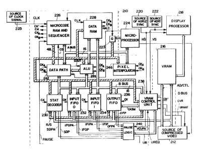
FIGURE 2 is a block diagram showing the video signal
processing circuitry 210 and associated peripheral
circuitry. In the present embodiment of the invention, the
circuitry 210 is imlplemented as a single integrated circuit.
The video signal processing system is described below
briefly, with reference to FIGURE 2 only, and then in
greater detail with reference to FIGURES 2-13. A third
section of this application reEers to FIGURES 14-23 and
describes how the various components of the system operate
in parallel to convert compressed video data in formats
'.~
~ 3 ~ r~ L ~J r`~
-8- RCA 81,636
such as those shown in FIGU~ES lA, 1~ and lC into pixel
values.
In FIGURE 2, a source of compressed video signal
212 provides video signal data ~7hich has been cGmpressed
using one or more of the video signal compression
techniques set forth above and which includes data that has
been statistically encoded. In this embodiment of the
invention, the data provided by the source 212 is applied
to a video random access memory (VRAM) 216 under control of
a VRAM control unit 238 that is internal to the video
signal processor 210. The source 212 used in this
embodiment of the invention is a compact disk read only
memory (CD ROM). It continually provides the compressed
data to the VRAM 216 in blocks of, for example, 32 bits
each. The VRAM control unit 238 coordinates data access
requests to the VRAM 216 from the source 212 and the
circuitry 210 to ensure that all of the data provided by
source 212 is written into the VRAM 216.
The VRAM 216 used in this embodiment of the
invention is composed of 128 of the ~PD41264 64K by 4-bit
dual port random access memory integrated circuits
manufactured by NEC Electronics Inc. The memory integrated
circuits are arranged in a matrix having 16 rows and eight
columns. In this configuration, the VRAM 216 provides 4
megabytes ~MB) of storage, arranged as 1,048,576 words of
32 bits each.
A display processor 218 accesses the VRAM 216 via
a serial output port to develop the active video portion of
a displayed video signal. The video signal processing
circuitry 210 and source of compressed video signals 212
access the data cells of the VRAM 216 via the standard
input-output bus. All access to the VRAM 216 by the video
signal processor 210 and display processor 218 is
controlled by the VRAM control unit 238 of the circuitry
210.
Data held in the VRAM 216 is provided to the
processing circuitry 210 by the statistical decoder 230 and
by the input first-in-first-out (FIFO) circuits 232 and
~ 3 ~ . a
-9- ~CA 81,636
234. Data is provided by the circuitry 210 to the VRAM 216
via the output FIFO circuitry 236. The data values
provided by the statistical decoder 230 and the input
FIFO's 232 and 234 are applied to data path circui-try 242,
an arithmetic and logic unit (ALU) 244 and a data RAM 228
via a bidirectional data bus B BUS. The bus B BUS is also
used to provide address values to the VRAM control unit
238. A second bidirectional bus, A BUS, is included in the
circuitry 210 to provide an alternate means for passing
lQ data values among the data path circuity 242, ALU 244 and
data RAM 228, and to provide data to, and accept data from
a pixel interpolator 246. In addition to the coupling set
fo_th above, the data bus A BUS is connected to a microcode
RAM and sequencer 226 and may be coupled to a
microprocessor 224.
In general terms, the circuitry shown in FIGURE 2
operates as follows. Compressed video signals, provided by
the source 212, are written into the VRAM 216. These
compressed video signals are accessed via the statistical
decoder 230 and the input FIFO's 232 and 234 under control
of the sequencing circuitry 226. The values provided by
the decoder 230 and the FIFO's 232 and 234 are applied to
thé data path 242, ALU 244 and pixel interpolator 246, also
under control of the sequencing circuitry 226, to expand
the compressed video signals and generate pixel values that
describe the encoded image. The generated pixel values are
written into the VRAM 216 via the output FIFO 236 as a
matrix having, for example, 240 rows and 256 columns.
These correspond to 240 lines of a video signal where each
line has 256 pixel values. This matrix is hereinafter
referred to as a bit-map. The bit-map is read from the
VRAM 216 by the display processor 218 to reproduce an
image. The display processor 218 used with this embodiment
of the invention converts the pixel values in the bit-map
into a video signal and adds the required horizontal and
vertical synchronization signals to enable the image to be
reproduced on a raster scan display device. To coordinate
transfers of data from the VRAM 216 to the display
-10~-3~ i3 RCA 81,636
processor 218, a horizontal line synchronizing signal, HS,
and a vertical field synchronizing signal, VS, are provided
to the processors 210 and 218 by respective signal sources
220 and 222. In a preferred embodiment of the invention,
these signals may be generated by the display processor
218.
In the present embodiment of the invention, a
source of clock signal 225 provides a 25 MHz clock signal,
CLK, to the microcode RAM and sequencer circuitry 226. The
circuitry 226 generates signals CK and CK', each having a
frequency of 12.5 MHz, a signal CKA, having substantially
the same frequency and phase as the signal CK, and a signal
CKB which is substantially antiphasal to the signal CK.
The clock signals CLK, CKA and CKB are applied to the data
RAM 228. The signals CKA and CKB are applied to the data
path 242, the ALU 244 and the pixel interpolator 246. The
signal CK is applied to the statistical decoder 230, the
input FIFO's 232 and 234, and to the output FIFO 236. The
signal CK' is applied to the VRAM control unit 238.
To simplify the explanation of the circuitry
shown in FIGURE 2, it is assumed that the source of
compressed video signals provides only encoded luminance
signals and, thus, that the circuitry 210 builds only one
bit-map, the luminance bit-map. In a practical system,
additional bit-maps for color information signals, for
example the I and Q color-difference signals, would be
generated as well.
As set forth above, the central control element
in the video signal processing circuitry 210 is the
microcode RAM and sequencer circuitry 226. FIGURE 3A is a
block diagram showing circuitry suitable for use as the
microcode RAM and sequencer 226. The microcode RAM 310 is
a conventional random access memor~ arranged as 128 words,
each of which has 96 bits. In normal operation, the
microcode RAM 310 provides a 96-bit word, addressed by the
seven MSB's of an address value held in an address register
322, to the input port of a register 312. The register 312
is conditioned by a signal hD provided by control circuitry
~ RCA 81,636
30B to load the value applled to its input port. Each of
the 96-bit values pro~ided by the microcode RAM 310
contains two 48-bit microcode control words or
instructions. One of these instructions, in the 48 MSB
positions o the register 312, is applied to one input port
of a multiplexer 314 and the o-ther instruction, in the 48
LSB positions of the register 312, is applied to a second
input port of the multiplexer 314. The multiplexer 314 is
conditioned by a single-bit signal provided by a flip-flop
318 to pass one of the 48-bit instructions to the input
port of the instruction register 316. The instruction
register 316 loads the microcode control word applied to
its input port in response to a signal LI provided by the
control circuitry 308.
The individual bits of the instruction register
316 are connected, via a bus MCW, to control input
terminals of each of the components of the video signal
processing circuitry 210. As the microcode control words
provided by the microcode RAM 310 sequence through the
instruction register 316, the individual components of the
circuitry 210 are conditioned to perform operations which,
in concert, convert the compressed video data into bit-map
pixel data. The function of each bit of the microcode
control word is described below in reference to FI~,URE 3C.
The clock signals CK and CK' used by the video
signal processor 210 are generated by circuitry included in
the microcode RAM and sequencer 226. The 25 M~z clock
signal CLK provided by the source 225 is applied to
frequency dividing circuitry 304 which divides the
frequency of the signal CLK by two to produce the 12.5 MHz
clock signal CK'. The signal CLK is further applied -to one
input terminal of an AND gate 306, the other input terminal
of which is coupled to an inverter 302 to receive an
inverted version of a signal HALT, provided by the
microprocessor 224. The output signal of the AND gate 306
is applied to frequency dividing circuitry 307 which
divides its frequency by two to produce the 12.5 MHz clock
signal CK. When the signal HALT has a logic zero value,
~ J~
-12- RCA 81,636
the signal CK ls a 12.5 MHz square-wave oscillatory signal.
~hen the signal HALT changes to a logic one, however, the
state of the signal CK is frozen at logic-one or
logic-zero, its state when the change in the signal HALT
occurred.
As set forth below, the eight LSB's of the
microcode control word define the NEXT ADDRESS field. In
any microcode control word, -this field contains the
address, in the microcode RAM 310, of the next microcode
lQ control word to be loaded into the instruction register
316. The value held in the NEXT ADDRESS field is applied
to the address register 322 via a multiplexer 320. The LSB
of the NEXT ADDRESS value is applied to the input terminal
D of the flip-flop 318. The address register 322 and the
flip-flop 318 are conditioned by the signal CK to load the
values applied to their respective input ports.
A signal CD, provided by the data path circuitry
242, as set forth below, is coupled to the reset input
terminal, R, of the flip-flop 318. The value of the signal
CD is controlled by the condition code select (COND CODE
SEL) field (described below) of the microcode control word.
This signal is used in the microcode RAM and se~uencing
circuitry 226 to conditionally change the sequence of
microcode control words applied to the instruction register
316. The signal CD represents a condition that occurred
earlier in the signal processing, for example, that the
output value of the ALU 2g4 is zero. When the selected
condition is true the output signal, Q, provided by the
flip-flop 318 becomes a logic-zero. This value conditions
the multiplexer 314 to pass the value held in the ~8 LSB
positions of the register 312 to the instruction register
316.
To understand how this circuitry may be used to
conditionally change the control flow of the microcode RAM
and sequencer circuitry 226, in other words to perform a
conditional branch operation, assume that a microcode
control word A has a non-zero value in its COND CODE SEL
field and a value of 81 in its NEXT ADDRESS field. When
f '~L i~ i~
-13- RCA 81,636
this microcode control word is loaded into the instruction
register 316, the eight-bit value in the NEXT ADD~ESS field
is applied to the address register 322 and the microcode
control words at addresses 80 and 81 in the microcode RAM
5 310 are loaded into the register 312. If the value of the
condition signal, CD, is logic-zero, the microcode control
word occupying the 48 MSB positions (address 81) of the
register 312 is the next to be used. Otherwise, the
microcode control word occupying the 48 LSB positions
(address 80) of the register 213 is next. Each of these
instructions has a distinct NEXT ADDRESS field and, so,
each defines a different sequence of microcode control
words, that is to say, a different functioning of the video
signal processor 210. Since the microcode RAM 310 provides
the next instruction for both possible values of the
condition code, no time is lost in fetching the next
microcode control word once the value of the condition is
determined.
The microcode RAM and sequencer circuitry 226 is
able to load microcode control words, supplied via the bus
A BUS, into the microcode RAM 310. Three 16-bit values,
each representing one-third of a microcode control word,
are successively applied to three registers 324. The first
16-bit value is stored into the register MRO, the second,
into the register MR1 and the third, into the register MR2.
Next, an address value, which may also be provided by the
VRAM 216 via the input FIFO 232 and data RAM 228, is
applied to the address register 322. The LSB of this
address value, the signal DXC, conditions a demultiplexer
326 to apply the 48-bit value provided by the three
registers MR0, MR1 and MR2 either to the 48 MSB positions
or to 48 LSB positions of the I/O bus for the microcode RAM
310. At the same time, a write enable signal, WE, is
pulsed to condition the ~AM 310 to store the 48-bit value
into the addressed memory cell.
The microcode control words written into the
microcode RAM 310 by these operations are provided from the
VRAM 216 via, for example, the input FIFO 232 and data RAM
-14- RCA 81,~36
circuitry 228. This ability to load microcode ins-tructions
from the VRAM 216 allows the source of compressed video 212
to provide both compressed data and the instructions needed
to decompress it to the video signal processor 210.
Initially, a bootstrap program may be loaded into the
microcode RAM 310 by the microprocessor 224 which may ~ake
control of the processor 210 as set forth below.
Responsive to the instructions in -this bootstrap program,
the microcode RAM and sequencer circuitry 226 loads the
instructions from the VRAM 216 which enable the processor
210 to decode the compressed video data.
FIGURE 3B is a timing diagram which illustrates
the operation of the microcode RAM and sequencing circuitry
226 when a microcode control word, MC, is stored into the
microcode RAM 310. In the timing diagram, the symbols To
through T5 represent six microcode instruction cycles.
Each instruction cycle begins and ends on a positive~going
transition of the signal CKA.
During the instruction cycle To~ the microcode
control word held in the instruction register 316 has a
value ~e.g. 8) in its A DST field indicating that the
16-bit value conveyed by the bus A BUS is to be stored into
the register MRO. In this instruction cycle, the value
MCO, the 16 LSB's of the microcode control word MC, is
gated onto the bus A BUS by, for example, the data RAM
circuitry 228. During the instruction cycle To~ the
register MRO is conditioned by the value of the signal A
DST to store the 16-bit value MCO provided by the bus A
BUS. The store operation occurs coincident with the
negative-going transition of the signal CKA, at the
midpoint of the instruction cycle To~ At substantially the
same time that the value MCO is s-tored into the register
MRO, the value in the NEXT ADDRESS field of the microcode
control word in the instruction register 316 is stored into
the address register 322 and the LSB of this address value
is stored into the flip-flop 318. The value stored in the
address register 322 conditions the microcode RAM 310 to
apply a 96-bit value, ~hich includes the next instruction,
-15 . RCA 81,636
to the register 312. This 96-bit value is loaded into the
register 312 coincident with the negative-going transition
of the signal LD which occurs slightly after the midpoint
of the instruction cycle To~ Responsive to the single-bit
value held in the flip-flop 318, the addressed 48 bit
microcode control word is applied to the input pork of the
instruction register 316. This microcode control word is
loaded into the instruction register 316 coincident with
the negative-going edge of the signal LI, occurring at the
end of the instruction cycle To~ During the instruction
cycle T1, the newly loaded microcode control word
conditions the register MRl to load a value MC1,
representing the middle 16-bits of the microcode control
word MC. In the same manner, a microcode control word
loaded into the instruction register 316 at the end of the
instruction cycle T1, conditions the register M~2 to load
the 16 MSB's of the microcode control word MC during the
instruction cycle T2.
The microcode control word loaded into the
instruc-tion register 316 at the end of the instruction
cycle T2 controls the transfer of the microcode control
word MC from the registers 324 to the microcode RAM 310.
The address used to store the microcode control word MC is
provided via the bus A BUS. At the start of the
instruction cycle T3, the A DST field of the microcode
control word in the instruction register 316 has a value of
11, indicating that the 16-bit value provided by the bus A
BUS is to be loaded into the address register 322.
Responsive to this value in the A DST field, the control
circuitry 308 applies a logic-one value, as the signal MXC
to the multiplexer 320 for approximately one cycle of the
signal CK. This signal conditions the multiplexer 320 to
apply the 8 LSB's of the value provided by the bus A BUS to
the input port of the address register 322. This address
value is loaded into the register 322 coincident with the
first negative-going transition of the signal CK in the
instruction cycle T3. The LSB of the value held in the
address register 322, the signal DXC, is applied to a
-16- ~- 3 ~ v? ~ RCA 81,636
control input terminal of a demultiplexer 326. The
demultiple-xer 326 is conditioned by the signal DXC having
values of logic-one or logic-zero to gate the 48-bit value
provided by the registers 324 onto the respective 48 MSB
positions or 48 LSB positions of the I/O bus.
The signal DXC is also used to generate a
separate write enable signal, via ~ND gates 311 and 313,
for each half of the microcode RAM 310. As set forth
above, the microcode RAM 310 is configured as 128 words
where each word has 96 bits. This memory is divided into
two halves. The left half contains the 48 MSB's of the 128
words and the right half contains the 48 LSB's of the 128
words. The signal DXC is combined, in the AND gate 313,
with the write enable signal WE, provided by the control
circuitry 308 to generate the write enable signal for the
left half of the microcode RAM 310. The signal DXC is
inverted and then logically ANDed with the signal WE by the
gate 311 to produce the write enable signal for the right
half of the microcode RAM 310.
In the present example, the signal DXC has a
value of logic one for approximately one period of the
signal CK at the start of the instruction cycle T3.
Conseguently, the microcode control word MC is written into
the 48 MSB positions of the cell in the microcode RAM 310
that has the address value represented by the seven MSB's
value held in the address register 322. The microcode
control word is written into the microcode RAM 310
coincident with the signal WE shown in FIGURE 3B.
Since the instruction cycle T3 performs a memory
write operation, the next microcode control word is not
loaded into the instruction register 316 during the first
period of the signal CK. This operation occurs during the
second period of the signal CK in the instruction cycle T3.
Coincident with the second positive-going transition of the
signal CK during the instruction cycle T3, the value of the
signal MXC is changed to logic zero, and an instruction
fetch operation proceeds as set forth in reference to the
instruction cycle To~ The microcode ~AM and seguencing
-17 - ~ ~ eJ ~ r~ ~ RCA 81,636
circuitry 226 operates in the manner described ln reference
to the instruction interval To for the instruction cycles
T4 and T5.
In the example set forth in FIGURE 3B, the
signals L~ and LI are inhibited during the first half of
the instruction cycle T3 to prevent erroneous microcode
control words from being loaded into the registers 312 and
316. In addition, the signals CKA and CKB are frozen by
the control circuitry 308 during the second half of the
instruction cycle T3 to put the video signal processing
circuitry in a paused state. This is done -to maintain
synchronous operation among the ALU 244, data RAM 228 and
pixel interpolator 246. Since the clock signals CKA and
CKB are disabled during the second half of the instruction
cycle T3, the internal states of the ALU 244, data RAM 228
and pixel interpolator 246 do not change in this time
period.
In the present embodiment of the invention, a
data read operation and a data write operation for the
microcode RAM 310 occur during separate periods of the
signal CK. Alternatively, the microcode RAM and sequencing
circuitry 226 may be designed to perform both operations in
a single period of the signal CK.
The control circuitry 308 is also responsive to a
signal PAUSE provided by the pause logic 240 to freeze the
clock signals CKA and CKB. In addition, the control
circuitry 308 is responsive to a signal, HALT, provided by
the microprocessor 224 to inhibit the signal CK,
effectively freezing the internal state of the entire video
signal processor 210 except for the VRAM control unit 238.
Using the signal HALT, the microprocessor 224 may
effectively assume the control functions of the video
signal processor 210 The signal HALT is applied to the
instruction register 316 to condition that register to
accept data from the bus MCW, provided by the
microprocessor 224 via the gating circuitry 223. The
microprocessor 224 causes the register 316 to load the
applied microcode control word by changing the signal HALT
- 18 ~ r~ RCA 81,636
from a logic-one to a logic-æero. D~ring the next period
of the clock signal CK after this change, the microcode RAM
and sequencer circuitry 226 causes this microcode
instruction to be executed. At the completion of this
clock period, the microprocessor 224 again changes the
signal HALT to a logic-one value and applies another
microcode instruction to the register 316. ~y operating in
this manner, the microprocessor 224 may cause the microcode
RAM and sequencer circuitry 226 to write data into any
register connected to the busses A BUS or B BUS or to load
a bootstrap program as set forth above. In addition, by
virtue of its connection to the bus A BUS and of a bus gate
520, described below in reference to FIGURE 5, the
microprocessor 224 may read the contents of any register or
either of the busses A BUS or B BUS.
FIGURE 3C is a diagram showing the format of a
microcode control word or instruction used by the microcode
RAM and sequencing circuitry 226. The control word
contains 13 fields. Each field is described below in terms
of the values that the field may have and the effect of
these values on the various components of the video signal
processor 210. The structure of the controlled components
is described below in reference to the various FIGURES
4-13.
Bits 0-7 of the microcode control word form the
NEXT ADDRESS field. The value represented by these bits is
the address, in the microcode RAM 310, of the next
microcode control word to be loaded into the instruction
register 316. During a given microcode instruction cycle,
the value represented by this field is stored in the
microcode address register 322.
The condition code select field occupies bits
8-10 of the microcode control word. These three bits
select one of the condition values held by a condition
register in the data path circuitry 242, described below.
The selected condition value, is the signal CD. This
signal is is used to perform a conditional branch
operation. As set forth above, a conditional branch is a
; ?~ ~3
-19- RCA 81,636
change in the sequence of microcode control words applied
to the instruction register 316, which occurs only when a
selected condition is met (i.e., when CD is logic-one).
Table l lists the condition code selection values and their
corresponding descriptions.
TABLE 1
Value in COND Description of the
CODE SEL Field Selected Condition
O NULL, no conditional branch
1 ALU carry out flag
2 ALU overflow flag
3 ALU output value is negative
4 ALU output value is zero
the value of the loop
counter in the data path 242
is zero
6 the LSB of the register
RO iIl the data path 242
7 the MSB of the register RO
in the data path 242
The bits 11-29 of the microcode control word
- contain four fields which control how data values are
transferred between the various components of the circuitry
210 via the busses A BUS and B BUS. Bits 11-15 are the A
SRC field. This field indicates which of the components
or registers within a component, acts as a source by
providing an output value to the bus A BUS. Bits 16-20 of
the microcode control word are the A DST field. This field
indicates which of the components, or registers within a
component, acts as a destination by accepting the value on
-20- ~ 3 ~ V 1 ~J ~ RCA 81,~36
the bus A BUS as its input value. Similarly, the field
SRC, bits 21-24, and B DST, bits 25-29, determine which
components of the circuitry 210 respectively provide values
to and accept values from the bus B BUS. The busses A BUS
and B BUS may convey both data and control information to
the various components of the video signal processor 210.
The registers which may be coupled to the busses A BUS and
B BUS and the control informa-tion conveyed by these busses
are described below in reference to the appropriate
component of the circuitry 210.
In general, the registers coupled to the busses A
BUS and B BUS include conventional decoding circuitry (not
shown) which is ccupled to one of the fields A SRC, A DST,
B SRC or B DST of the microcode control word. This
decoding circuitry produces a logic one value when the
control value which allows access to the register is
detected. The decoding circuitry that is responsive to the
A SRC field is inhibited by a value of logic-one in the LIT
SEL field, bit 31, of the microcode control word. When
this bit is logic-one, the value in the A SRC field is not
a valid A SRC value but a portion of an eight-bit literal
value as described below. For the registers controlled by
the fields A SRC and B SRC, the output value of decoding
circuits is coupled to an output enable input terminal of
the register. A logic-one value applied to this input
terminal conditions the register to apply its stored value
to the appropriate bus and a logic-zero value conditions
the register to present a high-impedance to the bus. For
the registers controlled by the fields A DST and B DST, the
output value of the decoding circuitry is coupled to a
data-load input terminal of the register. These registers
are conditioned to load the value conveyed by the
appropriate bus while the signal provided by the decoding
circuits has a logic-one value.
Bit 30 of the microcode control word is the field
DEC LOOP CTR. When this field has a value of 1, the loop
counter in the data path circuitry 242 is conditioned to
decrement its value during the microcode instruction cycle.
J ~h r.~ ~
-21- RCA 81,636
Bit 31 of the microcode control word is the field
LIT SEL. A value of 1 in this field conditions the
microcode RAM and seguencing circuitry 226 to treat the
bits 8-15 of the current microcode control word as a
literal value. This value is applied as a source value to
the eight LSB positions of the bus A BUS via the gate
circuitry 317 ~hich is enabled by the bit 31 of the
microcode control word. A zero value, from a digital value
source 315, is applied to the eight MSB positions on the
bus A BUS when the literal value is selected.
Bit 31 of the microcode control word is further
coupled to any of the registers which may use the bus A BUS
as a source, as set forth above, and to the condition code
logic 518 of the data path circuitry, described below.
Bit 32 of the microcode control word is the INT
~P field. When this bit has a logic-one value, the
microprocessor 224 is interrupted. This control function
may be used, for example, to signal the microprocessor 224
that a certain microcode instruction se~uence has been
completed.
Bit 33 of the microcode control word is the LATCH
COND CODE field. When this field has a value of 1, the
data path circuitry 242 latches the values of the various
conditions produced by the ALU 244 into the condition code
register. This control function is generally included in
an instruction preceding the instruction which selects a
condition for a conditional branch operation.
Bits 34 and 35 of the microcode control word are
the SHIFT CONT field. This field controls bit shifting
operations which are performed by the register RO of the
data path circuitry 242. Table 2 describes the function
performed by the register RO in response to the various
values of the SHIFT CONT field.
~3 ~ J
-22- RCA ~1,636
TABLE 2
Value Function
No shift
1 Shift all bits one bit
position toward the LSB.
The MSB of the value before
the shift operation is copied
into the MSB position of the
value produced b~ the shift
operation.
2 Shift all bits one bit
position toward the MSB. The
LSB of the shifted value is
zero.
3 Exchang~ the upper and lower
bytes of a value applied to
the register RO during the
current instruction cycle.
Bits 38-46 of the microcode control word
determine the function of the ALU 244 during the microcode
instruction cycle. Bit 47 is unused. To unders-tand the
function of the ALU 244 it is helpful to first describe its
structure. The ALU 244 shown in FIGURE 4A consists of five
parts, two operand input registers, 410 and 412, arithmetic
and logic circuitry (ALC~ 414, an output register 416 and a
demultiplexer 418. Register 412 is connected to the bus B
BUS and is enabled by a value of 1 in bit 36 of the
microcode control word, provided via the bus MCW, to load a
value from the bus B BUS. Register 410 is connected to the
bus A BUS and is enabled to load a value from that bus by
a value of 1 in bit 37 of the microcode control word. The
ALC 414 performs various arithmetic and logical operations
on the values held in the register 410 and 412. The
operation performed during any one instruction cycle is
controlled by the nine-bit value held in the field ALU oP
~3~n ~1 ~J~
-23- ~CA 81,636
CODE, bits 38-~6 of the microcode control word, which are
provided to the ALU via the bus MCW. In this nine-bit
field, the Yalue held in bits 38-44 determine the function
performed by the ALU according to Table 3. In Table 3, A
and B represent values held in the registers 410 and 412,
respectively, and CIN represents is the value applied to
the carry-in input terminal, CIN, of the ALC 414.
TABLE 3
Value of bits 38-44 Operation
31 A OR B
32 0
33 NOT A
34 No operation
36 NOT B
47 A XOR B
NOT A + CIN
67 A + CIN
68 NOT B + CIN
71 A - B - NOT CIN
76 B + CIN
77 B - A - NOT CIN
79 A + B + CIN
A AND B
In the above table, 'NOT' indicates a ones complement
operation and 'XOR' indicates an EXCLUSIVE OR operation.
Bits 45 and 46 of the microcode control word are
applied to a multiplexer 420 via the bus MCW to change
carry in signal, CIN, and to change the ADD operation
(opcode 74) to a dual-ADD-with-saturate operation. When
the bits 45 and 46 are both zero valued or when bit 45 is
zero and bit 46 is one, the multiplexer 420 applies a value
of zero from a digital value source 422 as the signal CIN.
When bit 45 is one and bit 46 is zero, the multiplexer 420
applies a value of one from a digital value source 424 as
the signal CIN. If both bit 45 and bit 46 have values of
one, the CIN input value provided by the multiplexer 420 is
the carry out condition value, COUT, provided by the
condltion code register of the data path circuitry 242.
-24- ~ ~h ~ RCA ~1,636
The signal CAR~Y OUT produced by the ALC 414 is
the carry -out signal provided by the MSB stage of the
16-bit adder shown in FIGURE 4B. The signal SIGN is the
MSB of the 16-bit result produced by the ALC 41~. The
signal OVERFLOW iS a logical combination of the sign bits
of the two input values applied to the ALC 414 and the sign
bit of the output value produced by the ALC 414. This
signal has a logic-one value when two negative input values
produce a positive outpu-t value or when two posltive input
values produce a negative Outpllt value. For all other
combinations of the three sign bits, the signal OVERFLOW
has a logic-zero value.
The ADD operation b~comes a dual-ADD-with-
saturate operation when bit 45 is zero and bit 46 is one.
In the dual-ADD-with-saturate operation, each of the 16-bit
registers 410 and 412 is treated as containing two
eight-bit values. The eight MSB's of the value held in the
register 410 are added to the eight MSB's of the value held
in register 412 and the result is stored in the eight MSB's
of the output register 416. Likewise, the eight LSB's of
the values held in the registers 410 and 412 are summed and
the result stored in the eight LSB's of the register 416.
Neither of these ADD operations can produce an overflow
condition. Instead, circuitry in the ALC 414 saturates the
sum. If the input values to the dual addition operation
are such that either the eight LSB sum or the eight MSB sum
would produce a negative overflow condition or a positive
overflow condition, the value provided for the sum is
saturated at 0 or 255 respectively, the smallest and
largest values that may be represented by an eight-bit
unsigned binary value.
To switch between providing a conventional ADD
and a dual-add-with-saturate operation, an unconventional
adder is used by the ALC 414.
FIGURE 4B is a block diagram of an adder which is
suitable for use in the ALC 414. Conventional 16-bit
arithmetic and logic circuitry would include a 16-bit adder
capable of summing two 16-bit two's complement numbers and
~ 3~
-25- RCA 81,636
a carry-in signal to produce a 16-bit -two's complement
output value and a carry-out signal. The circuitry shown
in FIGURE 4B is responsive ~o a signal, SPLIT, to operate
as a conventional 16-bit two's complement adder, when SPLIT
is zero or, as two independent eight-bit adders, in the
dual-add-with-saturate mode described above, when SPLIT is
one.
In FIGURE 4B, the two 16-bit input values applied
to the input ports A and B of the ALC 414 are each split
into an eight-MSB portion and an eight-LSB portion. The
eight MSB portions of the A and B input values are applied
to respectively different input ports of an adder 450. The
eight LSB portions of the A and B values are applied to
respectively different input ports of an adder 452. The
adders 450 and 452 used in this embodiment of the invention
are conventional eight-bit two's complement adders. The
carry-in input signal to the adder 452 is the signal CIN
applied to the ALC 414. The carry-in input signal to the
adder 450 is provided by an AND gate 454. This signal is
the logical AND of a carry-out signal, COO, pro~ided by the
adder 452 and a signal SPLIT, a logically inverted version
of the signal SPLIT, provided by an inverter 456. The
signal in the MSB position of the eight-bit output signal
provided by the adder 450 is the condition signal SIGN,
indicating the polarity of the value provided by the ALC
adder 414. The carry out signal, COl of the adder 450 is
the signal CARRY OUT provided by the ALC 414.
The eight-bit value provided by the adder 450 is
the two's complement sum of the eight MSB's of the values
applied to the input ports A and B of the ALC 414. The MSB
of this output value is applied to one input terminal of an
exclusive OR gate 472, the other input terminal of which is
coupled to receive the signal SPLIT. The output signal
provided by the exclusive OR gate 472 is concatenated to
the seven LSB's of the value provided by the adder 450 to
develop an eight-bit modified sum. When the signal SPLIT
is æero, the modified sum is an eight-bit two's complement
value representing the sum of two eight-bit two's
i i",~ J~
-26- RCA 81,636
complement values. When the signal SPLIT is one, however,
the modifi-ed sum is an eight-bit unsigned binary value
representing the sum of an eight-bit unsigned binary value
and an eight-bit offset-128 binary value.
The change in the type of input values applied to
the ALC adder is not a function of the adder circuitry but
a convention established for programming the video signal
processor 210. By this convention, when the signal SPLIT
has a value of zero, the values applied to the ALC adder
are conventional 16-bit two's complement values. When the
signal SPLIT has a value of one, however, one of the values
applied to each of the adders 450 and 452 is an eight-bit
unsigned binary value and the other value is an eight-bit
value in offset-128 notation. These values may be provided
by any register in any device which may act as a source for
the busses A BIJS or B BUS.
When the signal SPLIT is one, the eight-bit
unsigned binary input value may occupy a range of values
between 0 and 255 and the offset 128 value may occupy a
range of values between -128 and +127, respectively. Thus,
the modified sum may represent values between -128 and 382,
inclusive. However, since the modified sum in this mode is
an eight-bit unsigned binary number, only the values
between 0 and 255 are valid. The ALC adder shown in FIGURE
4B includes circuitry to detect values outside of this
valid range and to saturate, or limit, the value of the
modified sum to zero, for values less than zero and to 255
for values greater than 255.
An AND gate 470 develops a positive overflow
signal POVl which indicates that the value of the modified
sum is greater than 255. The three input signals to the
AND gate 470 are the signal SPLIT, the carry-out signal,
COl, from the adder 450, and the MSB of the eight-bit value
provided by the adder 450. The signal POVl is zero when
the signal SPLIT is zero or when the signal SPLIT is one
and the value of the modified sum is less than 256. The
signal POVl is applied to one input terminal of each of
eight NOR gates 474. The other input terminal of each of
~1 3 ~ g~ f~
-27~ RCA 81, 636
the NOR gates 474 is coupled to receive a respectively
different one of the eight bits of the modified sum.
A NOR gate 468 is responsive to the signal SPLIT,
the signal COl, and the MSB of the eight-bit value provided
by the adder 450 to generate a negative overflow signal,
NOVl. This signal indicates that the modified sum has a
value less than zero. The signal NOVl, is coupled -to one
input terminal of each of eight NOR gates 476. The other
input terminal of each of the NOR gates 476 is coupled to
receive a respectively different one of the signals
provided by the eight NOR gates 474. The eight output
signals of the NOR gates 476 are the eight MSB's of the
16-bit output signal of the ALC adder.
The adder 452 is coupled to value limiting
circuitry that is identical to that described above. The
eight output signals of eight NOR gates 466, which
correspond to the NOR gate 476, are the eight LSB's of the
16-bit output signal of the ALC adder.
When the bits 45 and 46 of the microcode control
word have respective values of zero and one, the signal
SPLIT is 1 and the ALC adder is conditioned to operate in
its dual-add-with-saturate mode. For all other
combinations of values of the bits 45 and 46 of the
microcode control word, the signal SPLIT is 0 and the ALC
adder is conditioned to operate as a conventional 16-bit
two's complement adder.
The following is an explanation of the operation
of the ALC adder in each of its two modes. When the signal
SPLIT is 0, the AND gate 454 is conditioned to apply the
carry-out signal from the output terminal CO0 of the adder
452 to the carry-in input terminal CIl of the adder 450
configuring the adders 450 and 452 as one 16-bit two's
complement adder. The zero valued SPLIT signal applied to
the exclusive OR gates 462 and 472 conditions these gates
to pass, unchanged, the MSB's of the eight-bit output
values provided by the respective adders 452 and 450 to the
respective NOR gates 464 and 474. The zero-valued signal
SPLIT applied to the AND gates 460 and 470 condition these
~ 3 ~
-~8~ RCA 81,636
gates to apply zero--valued positive overflow signals POV0
and POVl, respectively, to the respective NOR gates 464 and
474. In the same manner, the logic~one valued SPLIT signal
applied to the NOR gates 458 and 468 condition these ga~es
to apply zero-valued negative overflow signals, NOVo and
NOVl, respectively, to the respective NOR gates 466 and
476. The effect of the zero-valued signals PoV0 and NOVo
applied to the NOR gates 464 and 466 is to invert the
output value provided by the adder 452 twice and, so,
provide the value at the output port of the adder 452 as
the eight LSB's of the 16-bit value provided by the ALC
circuit. The same is true for the 8 MSB value provided by
the adder 450 to the output port of the ALC adder via the
NOR gates 474 and 476.
When the signal SPLIT has a logic-one value, the
signal SPLIT, provided by the inverter 456, has a
logic-zero value and the AND gate 454 is inhibited from
passing the carry-out signal from the adder 452 to the
carry-in input terminal, CI, of the adder 450. This
configures the adders 450 and 452 as two separate eight-bit
adders. The logic-one signal SPLIT applied to the
exclusive or gates 462 and 472 condition these gates to
logically invert the MSB's of the respective eight~bit
values provided by the adders 452 and 450. The ~SB is
inverted so that the eight-bit unsigned binary values
produced by each of the adders 452 and 450 properly
represent the sum of an eight-bit unsigned binary value and
an offset-128 binary value.
When the signal SPLIT has a logic-one value, the
AND gates 460 and 470 are enabled to produce the respective
positive overflow signals POV0 and POVl and the NOR gates
458 and 468 are enabled to produce -the respective negative
overflow signals NOVo and NOVl. When the negative overflow
signal NOVl is a logic-one, the output signals of the eight
NOR gates 476 all become logic-zero and the value of the
most signi~icant byte of the value produced by the ALC
adder is zero. When the signal POV1 is a logic-one, the
output values of the eight NOR gates 474 all become
-29- ~ 3 ~ v r ~ RCA 81,636
logic-zero. These signals are inverted by the NOR gates
476. Thus, the 8 MSB's of the output value of the ALC
adder all have values of logic-one. This corresponds to an
unsigned binary value of 255. The same analysis holds for
the signals NOVo and POV0 applied to the respective NOR
gates 466 and 464.
The result obtained by performing any of the
operations shown in Table 3 is stored in the output
register 416. This register may be coupled to one or both
of the busses A BUS and B BUS by the demultiplexing
circuitry 418, in response to appropriate values in the
fields A SRC and B SRC of the microcode control word.
The ALC used in this embodimen-t of the invention
is exemplary. One skilled in the art of digital logic
design may design and build alternative circuitry capable
of performing equivalent operations to those described
above.
The input reyisters 410 and 412 of the ALU access
the respective busses A BUS and B BUS independently of the
bus source and destination fields, A SRC, A DST, B SRC and
B DST, of the microcode control word. Consequently, in one
operation, the microcode RAM and sequencing circuitry 226
can direct that data values be transferred from a source to
a destination on each of the busses A BUS and B BUS, while
simultaneously directing the ALU to perform an operation on
one or both of the data values being transferred.
One source of input values to the ALU 244 and a
destination for output values from the ALU 244 is a
register file 510 in the data path circuitry 242. Figure 5
is a block diagram of the data path circuitry 242 used in
the present embodiment of the invention. The register file
510 used in this exemplary embodiment includes four general
purpose registers: RO, Rl, R2 and R3. Each of these
registers is coupled to both of the busses A BUS and B BUS.
Under control of the fields A SRC and B SRC of the
microcode control word, provided via the bus MCW, any one
of these registers may be enabled to apply a value to
either one or both of the busses. However, responsive to
~L 3 ~ ~ i rJ ~)
-30- RCA 81,636
the fields A DST and B DST, a register can serve as the
destination for only one of the busses A BUS and B BUS
during any one microcode instruction cycle. As set forth
above, the register RO includes circuitry responsive to the
SHIFT CONT field of the microcode control word ~o shift the
contents of the register to bit positions of greater or
less significance or to swap the eight MSB's and eight
LSB's of a value applied to the register.
The MSB and LSB of the register RO are connected
to respectively different input terminals of the condition
code register 512. In addition to these values, the
condition code register is coupled to receive a zero value
from a digital value source 513, the condition values SIGN,
ZERO, OVFLOW, and CARRY OUT provided by the ALU 244 and a
condition value which indicates that the value held by a
loop counter 514 is zero. The condition code register is
responsive to the LATC~ COND CODE field of the microcode
control word to store the values of the conditions produced
by the ALU 244 at the end of a microcode instruction cycle.
Other condition codes are latched into the condition code
register 512 asynchronously as they occur.
The condition code logic 518 is responsive to the
COND CODE SEL field of the microcode control word to select
one of the condition values held in the condition code
register 512 as the condition signal, CD, to be used to
per~orm a conditional branch operation in the microcode R~M
and sequencing circuitry 226, as set forth above. The
condition code logic is also responsive to the LIT SEL
field of the microcode control word to inhibit the
selection of a condition when the COND CODE SEL field is
being used along with the A SRC field to apply a literal
value to the bus A BUS.
The loop counter 514 is a 16-bit counter which,
under control of the fields A SRC and A DST of the
microcode control word, may serve either as a source or as
a destination for data values on the bus A BUS. The loop
counter 514 is decremented synchronous with the clock
signal CKB when bit 30 of the microcode control word has a
~ 3 ~ , a
-31- RCA 81,636
value of logic-one. This counter is used to count the
number of times that the instructions in an iterative loop
are performed by the microcode sequencer 226.
In general modes of operation, the busses A BUS
5 and B BUS are entirely independent. However, the video
signal processor 210 may be placed in a state in which
these two busses are joined into a single bus. This mode
is the HALT mode. The processor 210 may be placed in the
HALT mode by the microprocessor 224. The signal HALT
provided by the microprocessor 224 conditions a
bidirectional gating circuit 520 to j oin the two busses.
When in this mode, the microprocessor 224 may access any
register on the joined bus as a source or destination.
This feature facilitates testing the video signal processor
15 210 and allows the microprocessor 224 to configure the
processor 210 to start in any of a number of predetermined
states. While it is not shown in the present embodiment of
the invention, it is contemplated that the bus gate 520
may, alternatively, be controlled by a bit in the microcode
20 control word, for example, bit 47. Under control of a
microcode instruction, the gate 520 could be conditioned to
join the busses A BUS and B BUS to effect the transfer of
data provided by a source on one of the busses to a
destination which is coupled to the other bus.
In addition to the four general purpose registers
R0, Rl, R2 and R3, the video signal processor 210 uses the
data RAM circuitry 228 for temporary storage of data
values. FIGURE 6 is a block diagram showing details of the
data RAM circuitry 228 used with this embodiment of the
30 invention. The data RAM circuitry 22~ includes a 256 by 16
bit RAM 610, a register file 612, containing four address
registers DR0, DRl, DR2 and DR3, incrementing/decrementing
circuitry 622 and control circuitry 614. The control
circuitry 614 is responsive to the fields A SRC, A DST, B
35 SRC, and B DST of the microcode control word for
transferring data to and from the RAM 610 and for loading
and possibly incrementing or decrementing address values in
the various registers of the register file 612.
~ 3 ~ 3 ~ J ~"~
-32- RCA 81,636
In normal operation, the relevant fields of the
microcode control word are applied to the control circuitry
614 via the bus MCW. Values representing addresses for
accessing the RAM 610 are applied by, for example, the ALU
circuitry 244, to one input port of a multiplexer 616 as
the eight LSB positions of the bus A BUS. Another inpu-t
port of the multiplexer 616 is coupled to receive 8-bit
address values generated by incrementing/decrementing
circuitry 622 as set forth below. The multiplexer 616 is
conditioned by a signal MC1, provided by the control
circuitry 614, to provide one of the two address values
applied to its input ports to the registers DR0 through
DR3. The registers DR0 through DR3 are 8-bit
parallel-input parallel~output registers and are
conditioned to load values applied to their input ports by
the signals Lo~ Ll, L2 and L3, respectively. The output
values provided by the registers DR0 through DR3 are
applied to respectively different input ports of a
multiplexer 618. A control signal, MC2, provided by the
control circuitry 614 conditions the multiplexer 618 to
apply one of the address values held by the registers DR0
through DR3 to the input port of an 8-bit address register
620. Address values are loaded into the address register
620 responsive to a control signal LA provided by the
control circuitry 614. The address values held in the
register 620 are applied to an address input port of the
RAM 610 and to the input port of incrementing/decrementing
circuitry 622. The circuitry 622 is controlled by a signal
I/D provided by the control circuitry 614 to either
increment or decrement the address value applied to its
input port and to provide this modified address value to
the second input port of the multiplexer 616 as set forth
above.
The address value provided by the multiplexer 618
may be applied to the bus A BUS via a 3-state gate 619.
Responsive to a signal RO, provided by the control
circuitry 614, the gate 619 applies either the 16-bit value
provided by the multiplexer 618 and a source 621 or a high
~ 3 ~ i J
-33- RCA 81,636
impedance to the bus A BUS. The gate 619 is used in this
embodiment of the invention to allow the values held in
registers DR0 through DR3 to be applied to the bus A BUS as
an eight-bit data value. The eight MSB's of the value
applied to the bus A BUS are set to zero. The signal R0
conditions the gate 619 to apply a value to the bus A BUS
when the A SRC field of the microcode control word,
provided via the bus MCW, indicates that one of -the
registers DR0 through DR3 is the source of the data value
to be transferred via the bus A BUS.
Data values to be stored into the RAM 610 are
applied to the data RAM circuitry 228 via the two 16-bi-t
busses A BUS and B BUS. A 16-bit three-state gate, 624, is
responsive to a signal AIN generated by the control
circuitry 614 for applying either a data value ~rom the bus
A BUS or a high impedance to the I/O bus of the RAM 610.
An identical gate 626 is responsive to a signal BIN
generated by the control circuitry 614 for selectively
applying a data value from the bus B BUS or a high
impedance to the I/O bus of the RAM 610.
Data values applied to the I/O bus of the RAM 610
are written into data cells that are addressed by the
address value held in the address register 620. The
control circuitry 614 generates a write enable signal, WE,
which conditions the RAM 610 to write the data value into
the addressed cell during a given memory cycle.
Data values ~ay be read from an addressed cell of
the RAM 610 by holding the signal WE in a logic zero state
during at least a portion of a memory cycle. Values read
from the RAM 610 may be,applied to either one or both of
the busses A BUS or B BUS via the respective gates 628 and
630. The gates 628 and 630 are identical to the gates 6~4
and 626, they are responsive to the signals AOUT and BOUT,
respectively, which are provided by the control circuitry
614, to apply either the output value provided by the RAM
610 via its I/O bus or a high impedance to the respective
bus A BUS or B BUS.
r~
3~ ~ L J rJ 'RCA 81 636
As set forth above, the operation performed by
the data RAM circuitry 228 is determlned by the values of
the fields A SRC, A DST, B SRC and B DST of the microcode
control word. Table 4 is a descrip-tion of the operations
which may be performed in response to various values of
these four fields.
;J3 ~
-35- RCA 81, 636
TABLE 4
VALUE A SRC A DST B SRC B DST
2 *DR2 *DR2
3 *DR3 *DR3
4 *DR2++ *DR2+-~
*DR3+~ *DR3++
6 *DR2-- *DR2--
7 *DR3-- *DR3--
16 *DR0 *DR0
lO 17 *DRl *DRl
18 *DR0++ *DR0+~
l9 *DRl++ *DRl++
*DR0 - *DR0--
21 *DRl-- *DRl--
15 28 DR0 DR0
29 DRl DRl
DR2 DR2
31 DR3 DR3
The functions in the table 4 are encoded as in
the assembly language that is used to generate microcode
control words for the video signal processor 210. An
asterisk (*) preceding a register name indicates that the
value written or read is a value to be transferred to or
from the RAM cell addressed by the value held in the
register. If there is no preceding asterisk, the value
read or written is the 8-bit value held by the named
register. The "++" and "--" following a register name
indicates that the value in the register is incremented or
decremented, respectively, after the addressed memory cell
is accessed.
If the encoded operation is in the A SRC or B SRC
columns, then the operation is a read operation and the
output value is gated onto the bus A BUS or B BUS,
respectively. If the encoded operation is in the A DST or
B DST columns, then the operation is a write operation and
the input value i5 provided by the bus A BUS or B BUS,
respectively.
-36- RC~ 81,636
FIGURES 7A through 7E are timing diagrams which
illustrate various signals provided by the control
circuitry 614 in response to different values of the fields
A SRC, A DST, B SRC and B DST of the microcode control
word. To provide a comparison with other timing diagrams
in the present application, the clock signal CKA, provided
by the microcode RAM and sequencing circuitry 226 is shown
in each of the timing diagrams 7A through 7E.
FIG~XE 7A illustrates the timing of the various
signals produced by the control circuitry 614 in response
to a request to write an 8-bit value from the bus A BUS
into register DRO (i. e. A DST = 28). At a predetermined
time early in the instruction cycle, the value, VAL, to be
written into the register DRO i5 applied to the bus A BUS.
During this instruction cycle, the control circuitry 614
holds the signal MCl at a logic zero value conditioning the
multiplexer 616 to apply the value conveyed by the eight
LSB positions of the bus A BUS to the input ports of the
registers D~O through DR3. When the value applied to the
bus A BUS has stabilized, the control circuitry 614 pulses
the signal LO to condition the register DRO to load the
value applied to its input port. The commands for loading
the registers DR1, DR2 and DR3 are similar, the only
difference being that one of the respective signals L1, L2
or L3 is pulsed instead of the si~nal L0, as shown in
FIGURE 7A.
FIGURE 7B is a timing diagram showing signals
that are generated by the control circuitry 614 to transfer
the value held in the register DR0 to the eight LSB
positions of the bus A BUS (i.e. A SRC = 28). At a
predetermined time, shortly after the start of an
instruction cycle, the control circuitry 614 changes the
signal MC2 to have a zero value. This signal conditions
the multiplexer 618 to provide the value held in the
register DR0 to the input port of the gate 619. After
changing the signal MC2, the control circuitry 614 applies
a logic-one as the signal R0 to the gate 619. This signal
conditions the gate 619 to apply the value held by the
~ 3 ~ ~ L r ~ ~3
-37- RCA ~1,636
register R0 to the eight LSB positions of the bus A BUS and
to apply a value o~ zero to the eigh-t MSB positions o~ the
bus A BUS. Values in the registers DR1, DR2 or DR3 may be
read using a similar sequence of signal chanyes. The only
difference is that the value of MC2 is one, two or three,
respectively, instead of zero, as shown in FIGURE 7B.
FIGURE 7C illustrates the timing of several
signals used to read a value from a memory cell in the RAM
610 which is addressed by an address value held in register
DRO (i.e. A SRC = 16). For this operation, the control
circuitry 614 first changes the signal MC2 to have a zero
value, conditioning the multiplexer 618 to apply the
address value held by DR0 to the input port of the address
register 620. When this signal has stabilized, the control
circuitry 514 pulses the signal LA to load the address
value into the address regis-ter 620. When the address
value has propagated through address decoding logic of the
RAM 610, the addressed value is available on the I/O bus of
the RAM 610. The control circuitry 614 then gates this
value onto the bus A BUS by changing the value of the
signal AOUT to logic one. Values addressed by the register
DRl may be read using the same instruction sequence except
that the value of the signal MC2 is a one instead of a
zero. In this embodiment of the invention, data in the RAM
610 which is addressed by the registers DR2 or DR3 may be
read out only via the bus B BUS. The sequence of signals
to read these values may be obtained by changing the value
of MC2 in FIGURE 7C to be two or three respectively and by
using the gating signal BOUT instead of the signal AOUT.
FIGURE 7D illustrates the control signals which
condition the data RAM circuitry 228 to write a value
provided by the bus B BUS into a cell of the RAM 610 that
has the address value held in the register DR2 (i.e. B DST
= 2). As a first step in this operation, the control
circuitry 614 changes the value of the signal MC2 to two.
This conditions the multiplexer 618 to apply the address
value held in the register DR2 to the input port of the
address register 620. When the address value has
~ 3 ~ v ~ rd ~
38- CA 81,636
stabilized, the control circuitry 614 pulses the signal LA,
conditioning the address register 620 to load the value
applied to its input port. After the address value applied
to the RAM 610 has stabilized, the control circuitry 614
changes the signal BIN to a logic-one value, conditioning
the gate 626 to apply the value on the bus B BUS to the I/O
bus of the RAM 610. After a stabilization period, the
control circuitry 614 pulses the signal WE to condition the
RAM 610 to write the data on its I/O bus into the cell
having the address value applied to its address input port.
The signals used to write data values from the bus B BUS to
the RAM 610 using the address value in DR3 are the same as
those shown in FIGURE 7D except that the signal MC2 has a
value of three rather than two. In the present embodiment
of the invention, memory write operations using data on the
bus A BUS may only use the registers DR0 and DRl.
Consequently, to represent the signals used for these
operations (A DST = 28 or 29), the FIGURE 7D would be
changed in three ways: the signal B BUS would become the
signal A BUS, the value of the signal MC2 would be 0 or 1,
respectively, and the signal BIN would become the signal
AIN.
FIGURE 7E represent~ the same operation as in 7D
except that the address value is incremented after the data
value is stored. This operation is invoked when the value
in the field B DST is 4. The signals B BUS, MC2, LA, BIN
and WE are the same as those described in reference to
FIGURE 7D. In addition, shortly after changing the value
of the signal BIN, the control circuitry 614 changes the
signal I/D to have a logic one value. This signal
conditions the incrementing/~ecrementing circuitry 622 to
increment the value held in the address register 620 and to
apply the result to the second input port of the
multiplexer 616. When this value has stabilized, the
control circuitry 614 pulses khe signal MCl to apply the
incremented address value to the registers DR0 through DR2.
The control circuitry 614 pulses the signal L2, while the
~ i~ .L ~ r ~ lJ
-39- RCA 81,636
signal MCl is in a logic one state, to load the incremented
address value into the register DR2.
By holding the value of the signal I/D at logic
zero through the instruction cycle, the signals shown in
FIGURE 7E can be modified to decrement the address value
instead of incrementing it. Signals for the write
operations which use registers DR0, DRl and DR3 can be
obtained based on FIGURE 7E by modifying the signals B BUS,
MC2 and ~IN as set forth above in reference to FIGURE 7D.
Moreover, the signals used for the read-and-increment
operations (A SRC = 18 and 19 and B SRC = 4 and 5) and the
read-and-decrement operations (A SRC - 20 and 21 and B SRC
= 6 and 7) may be obtained by adding the signals MCl, I/D
and L2 from FIGURE 7E, with the appropriate modifications,
to the signals shown in FIGURE 7C.
In this embodiment of the invention, the pulse
signal shown in FIGURES 7A through 7E are generated by
selectively gating pulses of the 25 MHz signal CLK provided
to the data RAM circui~ry 228 by the source 225, and by
delaying the gated clock pulses via cascade-connected
gating elements. Even though the clock signal CLK is used
to generate its control signals, the data RAM circuitry 228
is responsive to the clock signals CKA and CKB to suspend
its operation when these clock signals are frozen by a
PAUSE or HALT command.
Using the FIGURES 6 and 7A through 7E, and the
related description, one skilled in the art of digital
signal processing circuit design could readily construct
suitable control circuitry 614 for use in the data RAM
circuitry 228.
As set forth above in reference to FIGURE lB, a
segment of an image may be encoded as a modification of a
corresponding segment from the previous image. This form
of encoding, called relative encoding, includes parameters
which describe an offset in the horizontal and vertical
directions between corresponding pixel positions in the two
segments (e.g., ~X and ~Y from FIGURE lB). As described
above, these offset values may be in terms of fractions of
rJ ,J
-40- RCA 81,636
the distance between adjacent pixels. In order to properly
decode images in which the fractional part o~ a pixel
offset value is non-zero, the video signal processor 210
desirably includes c.ircuitry for generating psuedo-pixels
from the pixels of the segment in the previous field.
These psuedo-pixels have values which approximate the
values of fractionally offset pixels. In the present
embodiment of the invention, the psuedo-pixels are
generated by the pixel interpolator 246.
The pixel interpolator 246 is configured to
calculate and store pairs of intermediate values
corresponding to pixels interpolated in the vertical
direction. These pairs of intermediate values are then fed
back to the interpolator, which, operating on successive
intermediate values, performs a horizontal in-terpolation to
produce pixel values that are interpolated both
horizontally and vertically. In other words, the pixel
interpolator 246 performs interleaved vertical and
horizontal interpolation calculations to produce the output
psuedo-pixel values.
FIGURE 8A is a block diagram showing circuitry
suitable for use as the pixel interpolator 246. In FIGURE
8A, the 16-bit bus A BUS is coupled to the respective input
ports of registers 802 and 812 to provide, respectively,
pixel data from, for example, the data RAM 228, and control
values from, for example, the ALU 244, to the pixel
interpolator 246. The registers 802 and 812 are
conditioned to load values from the bus A BUS when the A
DST field of the microcode control word has values of five
and four, respectively. The microcode control word is
applied to the pixel interpolator 246 via the control bus
MCW. The register 812 is coupled to control circuitry 814
which develops control signals for the various component
parts of the pixel interpolator 246 as described below.
The 16-bit value loaded into the register 802,
when the A DST field has a value of five, is interpreted by
the pixel interpolator 246 as two 8-bit pixel values having
successive positions on a horizontal line of the input
~ 3 ~ a
-41- RCA 81,636
video signal. Responsive to signals LRo and LR1, the
values held in the register 802 are alternately ~ransferred
to the respective 16-bit registers 804 and 806. In the
normal operation of the pixel interpolator 246, alternate
values applied -to the register 802 are corresponding pairs
of samples from successive lines of the input video signal.
For example, in FIGURE 9A where the triangles represent
pixels of the input video signal, the first value applied
to the register 802 would include the values representing
pixels S0O and S0l. The next successive value applied to
the register would include values representing pixels S10
and Sll, the corresponding pixel values from the next line
of the video signal.
As set forth below in reference to FIGURES 9A
through 9C, it is desirable for the pixel interpolator to
convert the pixel pairs stored in the registers 80~ and 806
from horizontally adjacent pixel values to pairs of
vertically adjacent pixel values. To this end, the eight
MSB positions of the registers 804 and 806 are coupled,
respectively, to the eight MSB positions and eight LSB
positions of a register 808 and the eight LSB positions of
the registers 804 and 806 are coupled, respectively, to the
eight MSB positions and eight LSB positions of a register
810. The registers 808 and 810 are conditioned to load the
values applied to their input ports by a signal XF which is
provided by the control circuitry 814. In the example set
forth above, the registers 808 and 810 contain the
respective pixel value pairs S00, S10 and S01, Sll
immediately after the control circuitry 814 has pulsed the
signal XF.
The 16-bit values provided by the registers 808
and 810 are applied to respectively different input ports
of a multiplexer 811. The multiplexer 811 is conditioned
by a signal MV, provided by the control circuitry 814, to
pass the 16-bit value applied to a selected one of its
input ports to the multiplexers 816 and 818. The eight MSB
positions of the output value of the multiplexer 811 are
applied to one input port of the multiplexer 816. The
-42- RCA 8],636
eight LSB positlons of the output value of the multiplexer
811 are applied to a corresponding input port of the
multiplexer 818.
The multiplexers 816 and 818 are conditioned by a
signal ML, provided by the control circuitry 814, to pass
either the two pixel values provided by the multiplexer 811
or two 8-bit vertically interpolated pixel values provided
by respective multiplexers 861 and 863. The pixel values
passed by the multiplexers 816 and 818 are applied to
registers 820 and 822, respectively. The registers 820 and
822 are responsive to the clock signal CKA provided by the
microcode RAM and sequencing circuitry 226, to load the
values applied to their respective input ports. The pixel
value held in the register 822 is subtracted from the pixel
value held in the register 820 by the subtracter 824. The
pixel difference value developed by the subtracter 824 is
applied to a multiplier circuit 825.
The multiplier 825, used in this embodiment of
the invention, is a programmable shift-and~add type of
multiplier. Circuitry suitable for use as the multiplier
825 is shown in FIGURE 8B. The value to be multiplied is
applied to two data paths, each of which contains three
serially coupled shifter-multiplexer pairs. Both the first
and second data paths convey nine-bit values. The
eight-bit value provided by the subtracter 824 is applied
as the eight MSB positions of the nine-bit v~lue applied to
the shifters 826 and 840 and to the multiplexers 828 and
842. The LSB of this value is zero. The extra bit of
precision is used in the multiplier 825 to mitigate
truncation errors which may occur due to the shift-and-add
multiplication teclmique.
The first data path includes a shifter 826 which
is coupled to receive the pixel difference value provided
by the subtracter 824 and to provide a bit-shifted version
of this value to one input port of a multiplexer 828. The
other input port of the multiplexer 828 is coupled directly
to the output port of the subtracter 824. The shifter 826,
and each of the shifters in the multiplier 825, provides
J~ ~x ~ o
-43- RCA 81,636
the eight MsB positions of its nine-bit input value as the
eight LSB positions of its nine-bi.t output value. A
logic-zero value is inserted in the MSB position of the
output value. One skilled in the art of digital signal
processing circuit design will recognize a shift of this
type as the equivalent of a division by two. The
multiplexer 828 is conditioned by a signal MA1 provided by
the control circuitry 814 to provide either the shifted or
unshifted value at its output port. The output port of the
multiplexer 828 is coupled to the input port of a shifter
830 and to one input port of a multiplexer 832. The
shifter 830 and mulkiplexer 832 are in the same
configuration as the shifter 826 and multiplexer 828. The
multiplexer 832 is controlled by a signal MA2 to
selectively provide the output value of the multiple~er 828
or a bit-shifted version of this output value. The
multiplexer 832 is coupled to provide its output value to a
shifter 834 and multiplexer 836 which are in the same
configuration as the shifter 830 and multiplexer 832. The
multiplexer 836 is controlled by a signal MA3 provided by
the control circuitry 814.
The second data path includes three
shifter-multiplexer pairs 840,842; 844,846; and 848,850,
each configured in the same manner as the shifter
multiplexer pairs in the first data path. The multiplexers
842, 846 and 8S0 are controlled by the respective signals
MBl, M~2, and MB3.
The output values provided by the multiplexer 850
are applied to a selective two's complementing circuit 852.
The circuit 852 is controlled by a signal CP provided by
the control circuitry 814 to provide either its input value
or the two's complement of its input value to the input
port of a register 854. The output values provided by the
multiplexer 836 of the first data path are applied directly
to the input port of a register 838. Both of the registers
838 and 854 are responsive to the clock signal CKB,
provided by the microcode RAM and se~uencing circuitry 226
to load the values applied to their respective input ports.
~ ~} ~ s~
~44- RCA 81,636
The output values provided by the registers 838 and 854 are
coupled to respectively different input por-ts of an adder
856. The values provided by the adder 856 are the output
values of the multiplier 825.
By controlling the values of the signals MA1,
MA2, MA3, MBl, MB2, MB3 and CP, the multiplier 825 may be
conditioned to multiply the values provided by the
subtracter 824 by scale factors having values between
one-eighth and one in steps of one-eighth. Table 5 lists
the values of the various control signals needed to produce
the scaled output values. In table 5, a control value of 0
for one of the MA or MB signals conditions the
corresponding multiplexer to pass the unshifted value while
a control value of 1 conditions the multiplexer to pass the
shifted value. A value of 1 for the signal CP conditions
the selective two's complementing circuitry 852 to
complement the value applied to its input port.
Table 5
SCAL~
20 MAl 2 3 MBl MB2 3 FACTOR
1 1 0 1 1 1 1 1/8
1 0 0 1 1 0 1 1/4
1 0 0 1 1 1 1 3/8
0 0 0 1 0 0 1 1/2
1 0 0 1 1 1 0 5/8
0 0 0 1 1 0 1 3/4
0 0 0 1 1 1 1 7/8
0 0 1 0 0 0
The values of the signals MAl, ~A2, MA3, M 1' 2 3
CP are generated by the control circuitry 814 in response
to the control value provided by the register 812.
The scaled pixel difference value provided by the
adder 856 is added to a pixel value provided by a register
857. The pixel value held in the register 857 is loaded
from the register 822 in synchronism with the clock signal
CKB provided by the microcode RAM and sequencing circuitry
J 3
-45- RCA 81,636
226. The function performed by the subtracter 824,
multiplier 825 and the adders 856 and 858 may be
represented by the equation (2)
R = SF * (A~B) ~ B (2)
where A and B are the pixel values held in the respective
registers 820 and 822. SF is the scale factor value
provided, for example, by the ALU 244 as a field in the
control value, and held in the register 812. The scale
factor SF is provided to the multiplier 825 via the MA, MB,
and CP signals. R is the value provided by the adder 858.
An algebraic manipulation of the equation (2) yields an
equation (3) which describes a convenkional linear
interpolation operation.
R = SF * A + (1 - SF) * B (3)
Thus, the combination of the subtractor 824, multiplier 825
and adders 856 and 858 is a linear interpolator.
The value provided by the adder 858 is applied to
the respective input ports of registers 860 and 862 and to
first input ports of the respective multiplexers 861 and
863. The second input ports of the multiplexers 861 and
863 are coupled to the respective output ports of registers
860 and 862. The registers 860 and 862 load the values
applied to their respective input ports coincident with the
negative-going transitions of the respective clock signals
~2 and ~1 The multiplexers 861 and 863 pass the value
provided by the adder 858 to the respective multiplexers
816 and 818 when the respective clock signals ~2 and ~1
have logic-one values and pass the value held in the
respective registers 860 and 862 otherwise. This
configuration o~ the registers 860 and 862 and multiplexers
861 and 863 enables simultaneous loading of the value
generated by the adder 858 into both the registers 860 and
820 or into the registers 862 and 822. The importance of
this capability is described below in reference to FIGURE
9C.
The pixel values provided by the adder 858 are
further coupled to both the eight MSB and eight LSB bi.t
positions of a 16-bit register 864. The eight MSB
-46- RCA ~1,636
positions of the register 864 are loaded in synchronism
with a signal LOl provided by the control circuitry 814 and
the eight LSB positions of the register ~64 are loaded in
synchronism with a signal LOo provided by the circuitry
814. The pixel values held in the register 864 are
transferred to a register 866 in response to a signal XO
provided by the control circuitry 814. These pixel values
are then applied to the bus A BUS, from the register 866,
under control of the A SRC field of the microcode control
word applied to the register 866 via the bus MCW.
In normal operation as a component part of the
video signal processor 210, the pixel interpolator 246
develops interpolated pseudo-pixel values, from the pixel
values of a previous image, as a step in developing pixel
values for the current image. FIGURES 9A through 9C
illustrate the operation of the circuity 246.
In FIGURE 9A, the triangular points S00 through
S07 and S10 through S17 represent corresponding pixel
values from two successive lines of the previous image,
which are provided from a bit-map in the VRAM 216 via the
input FIFO 232 and data path 242. The circular points Ioo
through Io6 represent interpolated pseudo-pixel values. As
illustrated in FIGURE 9A, the interpolated pixel values are
offset by one-quarter of the inter-pixel distance
horiæontally and five-eighths of the inter-pixel distance
vertically, with respect to the pixels in the previous
image.
FIGURE 9B illustrates how the pixel interpolator
246 is controlled by data values applied to the bus A BUS
to provide the psuedo-pixel values Ioo through Io3. In
FIGURE 9B, the time intervals To through T16 represent 17
successive instruction cycles of the video signal processor
210~ During the instruction cycle Tol the field A DST of
the microcode control word has a value of four,
35 conditioning the pixel interpolator 246 to load a 16-bit
control value provided, for example, from the ALU 244 via
the bus A BUS. The eight MSB positions of this 16-bit
control value condition the pixel interpolator 246 to
/ r ~ 3
-47- RCA 81,636
operate in its in-phase mode. In thls mode, the input
pixel values and their corresponding output pi~el values
both have even addresses in the VRAM 216. The pixel
interpolator 246 may alternatively operate in an
out-of-phase mode. In the out-of-phase mode, the input
pixel addresses are odd and the output pixel addresses are
even. The control value applied to the pixel interpolator
at time To further includes the values 5 and 2 in the bits
0-3 and 4-7, respectively. The value 2 corresponds to the
offset or scale factor 2/8 or 1/4 in the horizontal
direction and the value 5 corresponds to the of~set of 5/8
in the vertical direction. In the present example, the
values 5 and 2 are obtained from the fractional part of the
values ~X and ~Y of a relative code record such as that
shown in FIGURE lB.
During the instruction cycles Tl and T2, the A
DST field of the microcode control word has a value of five
and the pixel value pairs S0O, S0l and S10, S11
respectively, are applied to the register 802 of the pixel
interpolator 246. For the instruc-tion cycle T3 there is no
activity on the bus A BUS related to the pixel interpolator
246. During the instruction cycle T4, an invalid pair of
interpolated pixel values (x, x) is available at the output
port of the pixel interpolator 246. These values are
ignored by the video signal processing circuitry 210.
In the instruction cycles T5 and T6, the
respective pixel pairs S02, S03 and S12~ 13
the register 802 of the pixel interpolator 246. There is
no activity on the bus A BUS for the pixel interpolator 246
during the instruction cycle T7. In the instruction cycle
T8, a second invalid pair of interpolated pixel values is
available at the output port of the pixel interpolator 246.
These values are ignored. During the instruction cycles Tg
and T1o/ the respective pixel value pairs S04, S05 and S14,
Sl5 are applied to the register 802 of the pixel
interpolator 246. In the instruction cycle T11, there is
no activity on the bus A BUS related to the pixel
interpolator. During the instruction cycle T12, the A SRC
-~8- RC~ 81,636
field of the microcode control word has a value o~ five
conditioning the pixel interpolator Z46 to apply a 16-bit
value representing the interpolated pixel values Ioo and
Iol to the bus A BUS.
The instruction cycles T13 through T16 are
similar to the instruction cycles Tg through T12, the only
differences being the pixel values applied to and provided
by the pixel interpolation circuitry 246. Generally, the
microcode sequencer 226 repeats the operations in the
instruction cycles Tg through T12 using different input and
output pixel values, a number of times necessar~ to produce
all of the desired interpolated psuedo-pixel values.
The pixel interpolator 246 used in this
embodiment of the invention is a highly pipelined device.
The pipeline delay is 11 instruction cycles; the delay
between the application of the first input value, at T1,
and the presentation of the first valid output value, at
T12 .
FIGURE 9C is a signal timing diagram which
illustrates the timing of the various signals produced by
the control circuitry 814 in the example set forth in
FIGURE 9B. The signals CKA and CKB are anti-phasal clock
signals having a period that is substantially equal to one
instruction cycle time. The clock signals CKA and CKB are
applied to the pixel interpolator by the microcode RAM and
se~uencing circuitry 226.
All of the registers used in the pixel
interpolator circuitry shown in FIGURE 8 are negative-edge
triggered. In other words, they are all conditioned to
load the values applied to their input ports coincident
with negative going transitions of their respective clock
or load signals. The registers in FIGURE 8 are
synchronized to either clock signal CKA or clock signal
CKB .
Referring to FIGURES 9B and 9C, the control value
for the pixel interpolator is loaded into the register 81
during the instruction cycle To coincident with the
negative-going transition of the signal CKA. This value
J ~j
~49- ~CA 81,636
stabilizes in the control circuitry 814 by the end of the
instruction cycle To conditioning the circuitry 814 to
apply the values 1, 0, 0, 1, 1, 1, and 0 for the respective
signals MA1, MA2, MA3, MB1, MB2, MB3 and CP. These values
correspond to a scale factor of five-eighths, the scale
factor used in the present example for interpolating
between pairs of vertically aligned pixel values.
The first pair of pixel values, S0O and S0l, is
loaded into the register 802 during the instruction cycle
T1 coincident with the negative-going transition of the
signal CKA. These pixel values are transferred to the
register 806 at the end of the instruction cycle T1,
coincident with the negative-going edge of the signal LRo.
The second pair of pixel values, S10 and S11, is
loaded into the register 802 coincident with the
negative-going transition of the clock signal CKA which
occurs during the instruction cycle T2. These pixel values
are transferred to the register 804 coincident with the
~egative going transition of the signal LR1, occurring at
the end of the instruction cycle T2.
During the instruction cycle T3, the pixel values
held in the eight-MSB positions of the registers 804 and
806 are transferred to the respective eight MSB and eight
LSB positions of the register 808 and the pixel values held
in the eight LSB positions of the registers 804 and 806 are
transferred to the respective eight MSB and eight LSB
positions of the register 810. This transfer occurs
coincident with the negative-going transition of the signal
XF. The effect of this transfer is to convert the pairs of
horizontally aligned pixel values S0O, S0l and S10, S11 in
the respective registers 804 and 806 into pairs of
vertically aligned pixel values S10, S11 and S0O, S0l in
the registers 808 and 810, respectively.
During cycle T4, the control circuitry 814
changes the signals MAl through ~A3, MBl through MB3 and CP
to have values consistent with a scale factor of
five-eighths. The control circuitry 81~ further produces a
logic-one value as the signal MV, and a logic-zero value as
~ 3 ~
-50- RCA 81,636
the signal ML, conditioning the mul-tiplexer 811 which is
controlled by the signal MV and the multiplexers 816 and
818 which are controlled by the signal ML to couple the two
pixel values held in the register 810 to the respective
input ports of the registers 820 and 822. Coincident with
the negative going edge of the signal CKA, during the
instruction cycle T4, the pixel value S0O is loaded into
the register 822 and the pixel value S10 is loaded into the
register 820. During the remainder of the instruction
cycle T4, the values held in the registers 820 and 822
propagate through the subtracter 824 and the first and
second data paths of the multiplier 825, as set forth
above. The scaled pixel difference values provided by the
multiplexer 836 and selective two's complementer 852 are
loaded into the respective registers 838 and 854 coincident
with the negative going edge of the signal CKB occurring at
the end of the instruction cycle T4. At this same time,
the pixel value S0O from the register 822 is loaded into
the register 857.
In the instruction cycle T5, the pixel difference
values held in the registers 838 and 854 are summed by the
adder 856. The resultant sum is then added, by the adder
858, to the pixel value S0O provided by the register 857.
The sum provided by the adder 858, representing
five-eighths times the pixel value S10 plus three-eighths
times the pixel value S0O is stored in thP register 862
synchronous with the negative going edge of the signal ~1
Also during the instruction cycle T5, the pixel
values S02 and S03 provided via the bus A BUS are loaded in
to the register 802 and then transferred to the register
806 synchronous with the negative going transition of the
signal LRo.
During the instruction cycle T6, the pixel values
Sl2 and S13 are applied to the bus A BUS, loaded into the
register 802 and then transferred to the register 804
synchronous with the negative going transition of the
signal LR1.
-51- ~ 3 ~ `3 RC~ 81,636
At the midpoint of the instruction cycle T6, the
pixel values S0l and Sll held in the register 808 are
applied to the respective registers 822 and 820 via the
multiplexers 811, 816 and 818 and loaded into -these
registers responsive to the negative-going transition of
the signal CKA. These pixel values are propagated through
the subtractor 824, multiplier 825, register 857 and adder
858 during the remainder of the instruction cycle T6 and
the first half of the instruction cycle T7.
During the first half of the instruction cycle T7
the horizontally aligned pixel values S02, S03 and S12, S13
held in the respective register 806 and 804 are converted
into vertically aligned pixel pairs S02, S12 and S03, S13
which are stored into the respective register 810 and 808
synchronous with the negative going transition of the
signal XF occurring at the midpoint of the instruction
cycle T7.
The vertically interpolated pixel value (S0l,
S1l) provided by the adder 858 during the instruction cycle
T7 is loaded into the register 860 and, via the
multiplexers 861 and 816, into the register 820,
synchronous with the negative going edge of the signal CKA
occurring at the midpoint of the instruction cycle T7. The
signal ML, which Gonditions the multiplexer 816 to pass the
value provided by the multiplexer 861 to the register 820,
also conditions the multiplexer 818 to apply the vertically
interpolated pixel value (S0O, S10) provided by the
multiplexer 863 to the register 822. This pixel value is
loaded into the register 822 synchronous with the negative
going transition of the clock signal CKA occurring at the
midpoint of the instruction cycle T7, the signals MAl
through MA3, MBl through MB3 and the signal CP are changed
to have respective values of l,0,0,1,1,0 and 1. These
values correspond to a scale factor of one-fourth. During
the second half of the instruction cycle T7 and the first
half of the instruction cycle T8, the subtractor 824,
multiplier 825 and adder 858 horizontally interpolate a
pixel value from this pair of vertically interpolated pixel
~J~) . r ~ 1 3
-52~ RCA 81,636
values to generate the pixel value Ioo. This value is
stored in the eight LSB positions of the register 864
coincident with the negative going edge of the signal LOo,
occurring at the midpoint of the instruction cycle T8.
Also during the instruction cycle T8, the pair of
pixel values S02, S12 held in the register 810 are
transferred to the respective registers 822 and 820 via the
multiplexers 811, 816 and 818. These pixel values are
loaded into the registers 822 and 820 synchronous with the
negative going transition of the signal CKA occurring at
the midpoint of the instruction cycle T8. In the remainder
of the instruction cycle T8 and the first half of the
instruction cycle T~, the subtractor 824, multiplier 825
and adder 858 calculate a vertically interpolated pixel
value from the pair of pixel values S02, S12. This
interpolated pixel value is stored into the registers 862
and 822 synchronous with the negative going transitions of
the respective signals ~1 and CKA, both occurring at the
midpoint of the instruction cycle Tg. During the remainder
of the instruction cycle Tg, and the first half of the
instruction cycle T1o, the horizontally interpolated pixel
value, Iol, is developed from -the vertically interpolated
pixel values provided by the multiplexers 861 and 863. The
signals MA1 through MA3, MBl through MB3, and CP are set by
the control circuitry 814 to have respective values of
0,0,0,1,1,0 and 1 during the instruction cycle Tg. These
values correspond to a scale factor of 3/4. The pixel
value Iol is stored in the eight MSB positions of the
register 864 synchronous with the negative going transition
of the signal LO1 occurring at the midpoint of the
instruction cycle Tlo. The pixel pair Ioo, Iol is
transferred from the register 864 to the register 866 at
the end of the instruction cycle Tlo, synchronous with the
negative-going transition of the signal XO.
Also at the midpoint of the instruction cycle Tlo, the
pixel values S03 and S13, held in the register 808 are
loaded into the respective registers 822 and 820
synchronous with the negative going edge of the signal CKA.
? ~ J
-53- RCA 81,636
In the remainder of the ins-truction cycle T1o and the first
half of the instruction cycle T11, a vertically
interpolated pixel value is developed from the pi~el values
S03 and S13. This pixel value is stored into the
registers 860 and 820 synchronous with the negative going
transitions of the respective signals ~2 and CKA occurring
at the midpoint of the cycle T11.
During the instruction cycles Tg and T1o, the
respective pixel pairs S04, S05 and S1g/ 15
into the respective registers 806 and 804. At the midpoint
of the instruction cycle T11, these pixel values are
configured into vertically aligned pixel pairs S04, S14 and
S05, S15 which are stored in the respective registers 810
and 808.
In the second half of the instruction cycle T
and the first half of the instruction cycle T12, the
subtracter 824, multiplier 825 and adder 858 calculate the
pixel value I02, which is stored in the eight LSB positions
of the register 864 synchronous with the negative going
transition of the signal LOo occurring at the midpoint of
the cycle T12. Also at the midpoint of the instruction
cycle T12, the pixel pair Ioo, Io1 is applied to the bus A
BUS from the register 866.
During the instruction cycles T12 and T13, a
vertically interpolated pixel value is developed for the
pixel pair S04, S14. This interpolated pixel value is
loaded into the registers 860 and 820 synchronous with the
negative going transitions of the respective signals ~2 and
CKA occurring at the midpoint of the instruction cycle T13.
During the instruction cycles T13 and T14, the pixel value
Io3 is developed, using a scale factor of 3/4. This pixel
value is stored into the eight MSB positions of the
register 864 at the midpoint of the instruction cycle T14.
At the end of the instruction cycle T14 the pixel pair I02,
Io3 is transferred from the register 864 to the register
866. This pixel pair is applied to the bus A BUS during
the instruction cycle T16.
~ 3 ~ ~J ~
54- RCA ~1,636
The signals which drive the pixel in-terpolator
246 repeat every four instruction cycles. For example, the
signals for the instruction cycles T13 through T16 are the
same as those for the instruction cycles Tg through T12.
This sequence of signals repeats as many times as needed to
produce the desired number of psuedo-pixel values.
It should be noted that the first vertically
interpolated pixel value of a pair of pixel values which
are to be horizontally interpolated, alternately occupies
the re~isters 820 and 822. Consequently, the vertically
interpolated value which is added to the scaled vertically
interpolated difference value in the adder 858 alternates
between the first and second vertically interpolated values
in successive pairs of vertically interpolated values which
are combined to generate successive horizontally
interpolated values. To accommodate this alternation for
the horizontal interpolation calculations, the control
circuitry 814 alternately provid~s values for the signals
MAl through MA3, MB1 through MB3 and CP that correspond to
the scale factors SFH and (1-SFH~, respectively, where SFH
is the horizontal interpolation scale factor. In the
present example, when the first pixel value of a pair is in
the register 822, the horizontal interpolation factor of
one-fourth produces the correct psuedo-pixel output value.
When the first pixel value of a pair is in the register
820, however, the horizontal interpolation factor is
changed to three-fourths to produce the correct
psuedo-pixel output value.
In the description set forth above, the control
value applied to the pixel interpolator 246 during the
instruction cycle To conditions the interpolator to operate
in the in-phase mode. FIGURES 9D and 9E illustrate the
operation of the pixel interpolator in the out-of~phase
mode. As set forth above, the out-of-phase mode is
selected for the pixel interpolator 246 when the address of
an input pixel pair does not coincide with the address of a
16-bit value in the VRAM 216. This condition occurs when
~ 3~ ~3l r, 3
-55- RCA 81,636
the pairs of input piY~el values are split across a VRAM
word boundary. FIGUR~ 9E illustrates this situation.
The fundamental difference in the operation of the
pixel interpolator 246 in its in-phase and out-of-phase
modes are shown in fiyures 9E and 9F. As shown in FIGURE
9E, the pixel values Ioo and Io1 are available at the
output register 866 during the instruction cycle T16 rather
than during the cycle T12 as in the in-phase mode. Thls
change in operation is accomplished, as shown in Figure 9F,
by switching the signals LOo and LO1 and delaying the
signal XO by two periods of the signal CKA.
Although the pixel interpolator 246 is described
as a device for spatially interpolating pixel values for a
video image, it may also be used, more generally, for
averaging pixel values in either the horizontal or vertical
direction. This function is useful in various filtering
algorithms. For example, if the pixel values in FIGURE 9A
were to be applied to the pixel interpolator 246 in the
sequence SOO, SOl, SOO, SOl; S02~ S03~ S02' S03;
output values provided by the interpolator represent pixels
that are interpolated, or averaged in the horizontal
direction only.
Using the foregoing description and the FIGURES
8A, 8B and ~A through 9F, one skilled in the art of digital
video signal processing circuit design could readily design
and build suitable circuitry for use as the pixel
interpolator 246.
Pixel values and data held in the VRAM 216 are
accessed by the video signal processor 210 via the
statistical decoder 230, input FIFO's 232 and 234 and
output FIFO 236. All data read and data write operations
performed on the VRAM 216 using these devices, are
coordinated by the VRAM control unit 238. The statistical
decoder and each of the FIFOs has an associated VRAM
address and control value. The microcode sequencer 226
initializes the FIFO parameters after which, each FIFO runs
autonomously. From the point of view of the video signal
processor 210, there are three input instructions and one
-56- RC~ ~1,636
output instruction. The three input instructions are to
get pixel values from the sta-tistical decoder 230, input
FIFO 232 or input FIFO 234 and the output instruction is to
send a pixel value to the output FIFO 236. Each of these
devices automatically issues memory access requests for
32-bit words to and from the VRAM 216 and performs the
packing and unpacking needed to convert between eight or
16-bit pixel values and the 32-bit words stored in the VRAM
216, or to convert statistically encoded data into pixel
values.
The statistical decoder 230 translates variable
length encoded data held in the VRAM 216 into 16-bit binary
values which are applied to the bus B BUS in response to a
value of 14 in the B SRC field of the microcode control
word. Figure lOA is a block diagram of circuitry suitable
for use as the statistical decoder 230.
As set forth below in reference to Figure 13A,
the address value used to access the VRAM 216 for the
statistical decoder 230 is loaded into the VRAM control
unit from, for example, the data RAM 228, in two steps.
First, a value representing the 8 MSB positions of a 22 bit
address value is applied to the bus B BUS, while the B DST
field of the microcode control word has a value of 31.
Next the 14 LSB positions of the address value are loaded
from the 1~ MSB positions of a value applied to the bus B
BUS while the B DST field has a value of 30.
A value of 30 in the B DST field of the microcode control
word conditions control circuitry 1018 to reset the
statistical decoder 230 and to initiate a statistical
decoding operation.
A typical sequence of instructions would proceed as
follows. During two successive instruction cycles, the
eight MSB's and 14 LSB's, respectively, of an address value
are loaded into a pair of registers in the VRAM control
unit 238. In the same instruction cycle in which the 14
LSB's of the address value are loaded, the statistical
decoder 230 is reset and starts to operate.
r,J i3
-51- RCA 81,636
The reset operation is performed by control circuitry
1018 which applies a logic-one value as the signal RV to
the flip-flop 1017, marking the ei~ht-bit value held in the
output register 1016 as invalid. At the same time, the
control circuitry 1018 pulses a signal RDR, which is
applied to the set input terminal, S, of a flip-flop 1022.
This operation changes the output signal, SDR, of the
flip-flop 1022 to a logic-one value. The signal SDR is
applied to the VRAM control unit 238 via the bus R/S, to
request a read operation at the addressed location in the
VRAM 216. The output signal, SDR, of the flip-flop 1022 is
also applied to the control circuitry 1018 to indicate that
data has been requested from the VRAM 216.
When the VRAM control unit 238 has processed the
requested read operation and the VRAM 216 applies the
reguested 32-bit value to the bus D BUS, the VRAM control
unit 238 pulses a strobe signal SDS, provided via the bus
R/S. This signal conditions a register 1010 to load the
32-bit value from the bus D BUS. The signal SDS is also
applied to the reset input terminal R of the flip-flop 1022
to change the state of the signal SDR to logic-zero when
the 32-bit data value is loaded into the register 1010.
One-half of one period of the signal CK after the signal
SDS becomes logic-zero, the control circuitry 1018 provides
a signal SRL which transfers the 32-bit value from the
register 1010 to a shift register 1012 and resets the value
held in a counter 1020 to zero.
The statistical decoder 230 always begins its
decoding operation with the LSB of the 32-bit value read
from the VRAM 216. As described below, the input FIFO's
232 and 234 and the output FIFO 236 may specify a byte
position value as the first byte to be transferred from the
four-byte value which is read from or written to the VRAM
216. The byte-position value for these devices is encoded
as the two LSB positions of a 24-bit address value. In the
present embodiment of the invention, the statistical
decoder 230 ignores this byte-position value.
Consequently, data applied to the statistical decoder 230
~ 3 ~ c~ L ~ ~
58 - RCA 81,636
is assumed to begin with the LSB position of a 32-bit word
in the VRAM 216.
Whenever the control circuitry 1018 pulses the
signal SRL to transfer a 32-bit data value from the
register 1010, it also pulses the signal RDR to condition
the VRAM control unit 238 to increment the stored address
value and provide the next successive 32-bit data value
from the VRAM 216 to the register 1010. One-half of one
period of the signal CK after pulsing the signals SRL and
RDR, the circuitry 1018 applies a logic-one value as the
signal EN to the statistical decoding circuitry 1014,
enabling the circuitry 1014 to begin decoding the value
held in the shift register 1012.
The statistical decoding circuitry 1014 used in
this embodiment of the invention may, for example, be o~
the type described in U.S. Patent No. 4,396,906 entitled
"Method and Apparatus for Digital Huffman Encoding". When
enabled, the circuitry 1014 gates the system clock signal
CK as a signal SRCK to the shift register 1012 and to the
counter 1020. The shift register 1012, provides one bit
of the value it holds for each cycle of the signal SRCK,
starting with the LSB position and continuing toward to
the MSB position. As each bit is provided by the shift
register 1012, the value in the counter 1020 is
incremented by one.
When the statisti~al decoding circuitry 1014 has
processed a sufficient number of bits to produce a 16-bit
output value, in other words, when it has decoded one
variable-length encoded value, it applies the decoded
16-bit value to the input port of the output register 1016
and applies a logic one value, as the signal RDY, to the
control circuitry 1018. The control circuitry 1018 then
pulses the signal ORL to load the value provided by the
circuitry 1014 into the output register 1016 and to set
the flip-flop 1017, marking the data held by the register
1016 as valid.
This decoding operation is complete when the
value held in the output register 1016 is accessed as a
c~
-59- RCA 81,636
source for the bus B BUS by the use of a microcode control
word having a B SRC field with a value of 14 or 15. On the
next clock period after the control circuitry 1018 detects
this value in the B SRC field, it pulses the signal RV,
marking the data held in the register 1016 as invalid. A
value of 14 for BSRC indicates that more data values are
expected while a value of 15 indicates that the value
accessed is the last in the sequence.
The analysis set forth above assumes that the
data in the register 1016 is not accessed until it is
valid. If an attempt is made to access invalid data (e.g.
B SRC = 14 and ORV = O), the control circuitry 1018 pulses
the signal PR. The signal PR is applied to the set input
terminal, S, of a flip-flop 1023. When the signal PR is
pulsed, the output signal SDPA of the flip flop 1023
changes to a logic-one value. This signal is applied to
the pause logic 240 to cause the micrGcode RAM and
sequencer 226 to place the video signal processor in a
paused state. The signal SDPA is further applied to one
input terminal of an AND gate 1025, the other input
terminal of which is coupled to receive the signal SDR. I f
both SDR and SDPA have logic-one values, the output signal,
SDP, of the AND gate 1025 becomes logic-one. This signal
is applied to the VRAM control unit 238 via the pause logic
240 to increase the priority of the requested read
operation. The signal SDP is an urgent read operation
request signal from the statistical decoder 230. The
signal SDPA becomes a logic-zero, releasing the paused
state, when the control circuitry 1018 pulses the signal
ORL to mark the value held in the register 1016 as valid.
The example set forth above describes the
internal operation of the statistical decoder 230 in
producing one 16-bit output value. Typically, the decoder
230 will produce a sequence of such values. To produce the
first value in this sequence, the circuitry shown in Figure
10 operates as described above. Once that value has been
transferred to the output register 1016, the control
circuitry 1018 applies a logic-one value as the signal EN,
-60~ RCA 81,636
enabling the statistical decoding circui-try 1014 to produce
the next ~ecoded value. When the first decoded value is
accessed from the output register 1016 and the signal ORV
is changed to have a logic zero value, the con-trol
circuitry 1018 pulses the signal ORL to load the second
value. If the second value has not been decoded when the
first value is accessed, the control circuitry 1018 does
not pulse the signal ORL until the signal RDY is changed to
a logic-one value by the statistical decoding circuitry
1014. This sequence of opera-tions repeats until the value
in the output register 1016 is accessed using a value of 15
in the BSRC field of the microcode control word. When the
value in the output register 1016 is accessed in response
to a microcode control word having a value of 15 in its
BSRC field, the control circuitry 1016 terminates the
operation of the statistical decoding circuitry 230 by
changing values of the signal EN to a logic-zero. Data may
not be accessed using the statistical decoder 230 until a
new value is established for the 14 LSB positions of the
VRAM address value used by the decoder 230.
In any of the decoding operations described
above, 32-bit data values are provided from the VRAM 216 to
the register 1010 as required. When the counter 1020 is
incremented to have a value of 31, indicating that the MSB
of the current 32-bit value has been applied to the
circuitry 1014, the control circuitry 1018 pulses the
signal SRL to transfer the next 32-bit value from the
register 1010 to the shift register 1012 and to reset the
value of the counter 1020. At the same time, the control
circuitry 1018 pulses the signal RDR to request the next
sequential 32-bit value from the VRAM 216.
If, when the value in the counter 1020 equals 31,
the value of the signal SDR is a logic-one, the control
circuitry 1018 cannot transfer a value from the register
1010 to the register 1012 because the read operation to
fill the register 1010 has not yet been completed. In this
instance, the control circuitry 1018 changes the signal EN
to have a logic-zero value, to disable the decoding
-61- RCA 81,636
circuitry 1014. When the requested read operation is
completed, the control circuitry 1018 pulses the signal SRL
to transfer the new 32-bit value from the register 1010 to
the register 1012, changes the value of the signal EN to a
logic-one and pulses the slgnal RDR. These signals enable
the statistical decoder 230 to resume normal operation, and
request a new 32-bit value from the VRAM 216.
FIGURE lOB is a timing diagram which shows the
relative timing of signals produced b~ the control
circuitry 1018 as two data values are decoded.
From the Figures lOA and lOB and from the
description set forth above, one skilled in the art of
digital signal processing circuit design could readily
design and construct suitable circuitry for use as the
statistical decoder 230.
The input FIFO's 232 and 234 allow the video
signal processor 210 to read a random eight-bit or 16-bit
value or to read a sequence of eight-bit or 16-bit values
for the VRAM 216 for processing by its pixel processing
elements. In either the random or the sequential mode, the
microcode control word instructions executed by the
microcode RAM and sequencing circuitry 226 apply an initial
address value to the VRAM control unit 238. The selected
input FIFO accesses the VRAM 216 via the VRAM control unit
238 and provides the requested value or values to the bus B
BUS without further intervention by the microcode RAM and
sequencer 226.
The starting address values for the input FIFO's
232 and 234 supplied by, for example, the data RAM 228, are
established in the VRAM control unit 238 in the same manner
that address values are specified for the statistical
decoder 230. The eight MSB positions of an address value
are transferred via the bus B BUS to the address registers
for the respective input FIFO's 232 and 234, responsive to
the B DST field of microcode control words having
respective values of 23 and 27. The 14 LSB positions of an
address value for the input FIFO's 232 and 234 are
transferred from the 14 MSB positions of values applied -to
-62- RCA 81,636
the bus B BUS when the B DST field of the microcode control
word has values of 22 and 26, respectively. The two LSB
positions of the values applied to the bus B BUS when the B
DST field has values of 22 and 26 are stored internally in
the respective input FIFO's 232 and 234. The value
represented by these two bits points to a particular byte
of the four byte value provided by the VRAM 216 as the
first byte to be provided to the bus B BUS.
Figure llA is a block diagram showing circuitry
suitable for use as either of the input FIFO's 232 or 234.
The circuitry is described below for the input FIFO 232.
~ariations in the description to cover the input FIFO 234
are indicated parenthetically where appropriate. The
circuitry shown in Figure llA is described in terms of a
normal sequence of operations, where the input FIFO is set
to operate in the random mode. This description is
followed by an explanation of the changes in the sequence
of operations when the FIFO is set to operate in the
sequential mode.
The first step in the sequence is to apply a
control value to the bus B BUS using a microcode control
word having a value of 21 (29 for the FIFO 234) in its B
~ST field. Responsive to this B DST value, the control
value provided, for example, by the ALU 244, is loaded into
a register 1112. The control value used in this example
conditions the input FIFO 232 to operate in its random mode
as opposed to its sequential mode and to provide eight-bit
values as opposed to 16-bit values to the bus B BUS.
The next step in the sequence is to establish the
address value for the FIFO 232 in the VRAM control unit 238
as set forth above. A register 1110 internal to the the
FIFO 232 is responsive to the B DST field of the microcode
control word having a value of 22 (26) to load the byte
position value, that is, the two LSB's o~ the 16-bit
address value provided via the bus B BUS. Control
circuitry 1116 is also conditioned by this value of the B
DST field to reset the input FIFO 232 to an initial state
and to initiate a VRAM read operation.
~3 ~
-63- RCA 81, 636
In this reset operation, the control circuitry
1116 pulses a signal CO to reset a flip~flop 1134. One-half
of one period of the signal CK later, the control circuitry
1116 pulses the signal PC to load the byte position value,
BP, from the register 1110 into the counter 1128 and
flip-flop 1132. One-half of one period of the signal CK
after this operation, the control circuitry 1116 pulses a
signal IR, which is applied to the set input terminal, S,
of a flip-flop 1133. The signal, IFOR, provided by the
flip-flop 1133 is applied to the VRAM control unit 238 via
the control bus R/S, to condition the VRAM control unit 238
to initiate a read operation for the addressed memory
location in the VRAM 216. The signal IFOR is also applied
to the control circuitry 1116 to indicate that a read
operation is in progress.
When the VRAM control unit 238 has processed the
read operation, and the VRAM 216 has applied the requested
data to the bus D BUS, the VRAM control unit pulses a
strobe signal IFOS, provided via the bus R/S, to condition
a register 1118 to load the 32-bit value from the bus D
BUS. The signal IFOS is further applied to the reset input
terminal, R, of the flip-flop 1133, to reset the internal
state of the flip-flop 1133 and, so the signal IFOR, to a
logic-zero value, indicating that the memory read operation
is complete.
During the first period of the signal CK after
the signal IFOR becomes a logic zero, the control circuitry
1116 pulses a signal LR to transfer the 32 bit value held
in the register 1118 to the register 1120.
The bits of the register 1120 are divided into
four eight-bit segments, B0, Bl, B2, and B3 encompassing
bits 0-7, 8-15, 16-23 and 24-31, respectively. The
eight-bit values B0, Bl, B2 and B3 are applied to
respectively different input ports of a multiplexer 1124.
The multiplexer 1124 is controlled by a value provided by
the counter 1128 or by the multiplier 1130 to provide one
of the four values applied to its input port to the eight
LSB positions of the output register 1114.
-64~ v RCA 81,636
In the present exarnple, the control value in the
register lil2 indicates that eight-bit values are to be
provided by the output register 1114. Consequ~ntly, the
control circuitry 1116 applies a logic-one value as the
S signal MXC to a multiplexer 1126. This value of the signal
MXC conditions the multiplexer 1126 to apply the value held
in the counter 112~ to the control input port of the
multiplexer 1124. This value, which is the value of the
first byte position, conditions the multiplexer 1124 to
apply the addressed byte to -the eight LSB positions of the
output register 1114. In the next successive period of the
signal CK after pulsing the signal LR, the control
circuitry 1116 pulses the signals LL and RH to load the
value applied by the multiplexer 1124 into the eight LSB
positions of register 1114, reset the eight MSB positions
of the register 1114 and to set the flip-flop 1134. Since
the flip-flop 1134 is set, its output signal, OV is a
logic-one indicating that the value in the output register
1114 is valid.
The sequence of operations for this example is
completed when the microcode RAM and sequencing circuitry
226 executes a microcode control word in which the B SRC
field has a value of 12 (13 for the input FIFO 234). This
value, applied to the register 1114, enables that register
to provide its stored value to the bus B BUS. The control
circuitry 1116 is also responsive to a value of 12(13) in
the B SRC field to pulse the signal CO and thereby reset
the flip-flop 1134, marking the value in the output
register 1114 as invalid.
If the value in the control register 1112
indicates that 16-bit values are to be provided to the bus
B BUS, the control circuitry 1116 applies a logic-zero
value, as the signal MXC, to the control input terminal of
the multiplexer 1126. This control value conditions the
3~ multiplexer 1126 to apply the value provided by the
multiplier 1130 to the control input port of the
multiplexer 1124.
-65~ RCA 81,636
The multiplier 1130 is coupled to the output
terminal o~ the flip-flop 1132. As set forth above, the
flip-flop 1132 is preset to the value of the MSB of the
byte-position-v~lue stored in the register 1110. This
one-bit value is shifted one bit position toward greater
significance by the multiplier 1130 (i.e multiplied by
two~. Thus, the value provided by the multiple~er 1124 is
either a two or a zero. Accordingly, the multiplexer
applies either byte B0 or byte B2 to the eight LSB
positions of the output register 1114.
The output terminal of the flip-flop 1132 is
further coupled to the control input terminal of a
multiplexer 1122. The multiplexer 1122 is coupled to the
B3 and Bl sections of the register 1120. When -the value
provided by the flip-flop 1132 is a logic zero or a
logic-one the multiplexer 1122 applies the value held in
the respective Bl or B3 sections of the register 1120 to
the eight MSB positions of the register 1114. In the
16-bit mode, the control circuitry 1116 simultaneously
pulses the signals LL and LM to load both the selected
eight MSB ' s and eight LSB ' s into the register 1114. When
this value is accessed, via a microcode control word having
a value of 12 (13) in its B SRC field, the 16 MS~'s or the
16 LSB 's of the 32-bit value provided by the VRAM 216 may
be read. If the byte position value held in the register
1110 is a 1 or a 3, it will be interpreted as a 0 or a 2,
respectively; a 16-bit value including bytes Bl and B2
cannot be provided by the input FIFO's 232 and 234 used
with this embodiment of the invention.
In the examples set forth above, the control
value applied to the input FIFO conditions it to operate in
its random mode. In this mode, the FIFO provides only the
addressed value to the bus B BUS. In its sequential mode,
the input FIFO 232 or 234 may provide a sequence of values
starting with a value having the specified address in the
VRAM 216 and continuing through successively greater
address values. The operation of the FIFO's 232 and 234 in
-66- i ~J '' t~ ~ RCA 81~636
the sequential mode is described in terms of the
differences from its operation in the random mode.
A first difference between the random and
sequential modes is that, in the sequential mode, whenever
the control circuitry 1116 pulses the signal LR to load a
new 32-bit value into the register 1120, it also pulses the
signal IR to request -the next 32-bit value from the VRAM
216.
In the random mode, the counter 1128 and
flip-flop 1132 were used only as registers to hold the
byte-position value stored in the register 1110. In the
sequential mode, the counter 1128 and flip-flop 1132 are
used to sequentially provide successive eight-bit or 16-bit
values, respectively, from the register 1120 to the output
register 1114. The counter 1128 is a conventional two-bit
binary counter having a preset-value input port and a
preset input terminal. When the signal applied to the
preset input terminal is pulsed, the counter 1128 is
conditioned to load the value applied to its preset-value
input terminal as its internal value. The flip-flop 1132
is a conventional trigger type or T flip-flop. This
flip-flop has preset-value and preset input terminals which
are conditioned by the signals applied thereto to operate
as described above. A clock signal, CCK, provided by the
control circuitry 1116 is applied to clock signal input
terminals of both the counter 1128 and the flip-flop 1132.
In response to successive pulses of the clock signal CCK,
the counter 1128 cycles its internal value, CV through the
values 0,1,2 and 3. The flip-flop 1132 changes its
internal state between 0 and 1 in response to successive
pulses of the signal CCK. In this embodiment of the
invention, when the input FIF0 is in its sequential mode,
the signal CCK is the same as the signal LL, when the FIFO
is in its random mode, the signal CCK has a constant
logic-zero value. Conse~uently, as soon as a value is
loaded into the output register 1114, khe counter 1128 or
flip-flop 1132 condition the multiplexers 1122 and 1124 to
apply the next se~uential value to the input port of the
RCA 81,636
-67-
register 1114. Since the value applied to the input port
of the register 1114 is changed each time a new value is
loaded into the output register 1114, this applied value
may be loaded into the output register as soon as the value
in the register 1114 is applied to the bus B BUS.
The output value, CV, of the counter 1128 is
applied to the control circuitry 1116. The control
circuitry 1116 monitors this signal to determine when to
transfer a 32-bit value from the register 118 to the
register 1120. When the control value held in the register
1112 indicates that the input FIFO 232 is operating in its
eight-bit mode, the control circuitry 1116 pulses the
signal LR to transfer a 32-bit value from the register 1118
to the register 1120 coincident with the value of the
signal CV changing from one to zero (i.e. when the MBS of
the signal CV changes from one to zero). When the input
FIFO is operating in a 16-bit mode, the control circuitry
1116 pulses the signal LR when the value of the signal CV
changes from one to two or from three to zero (i.e. when
the LSB of the signal CV changes from one to zero).
The examples set forth above assume that the VRAM
control unit 238 and VRAM 216 provide 32-bit data values to
the input FIFO's 232 and 234 in a steady stream. If this
stream should be interrupted and, for example, the signal
IFOR has a value of logic-one, indicating that a read
operation is in progress, when the value of the signal CV
changes from three to zero, the control circuitry 1116 does
not pulse the signal LR. In this instance, the circuitry
1116 freezes its internal state until the signal IFOR
changes to a logic-zero value, indicating that the
requested VRAM read operation has occurred and, thus, that
the register 1118 contains valid data. When the signal
IFOR becomes zero, the control circuitry 1116 resumes its
operation.
If, while the internal state of the control
circuitry 1116 is frozen, a request is received to read the
contents of the register 1114 onto the bus B BUS (i.e. BSRC
= 12), the control circuitry 1116 pulses a signal IP which
-68- RCA 81,636
is applied to the set input terminal, S, of a flip-flop
1135. Thi-s action changes the state of the signal, IFOPA,
provided by the flip-flop 1135 to a logic-one. The signal
IFOPA is applied to the pause logic circuitry 240 which
conditions the microcode RAM and sequencer circuitry to
place the video signal processing circuitry 210 into the
paused state. As set forth above, in reference to FIGURE
3A, the clock signals CKA and CKB are disabled in the
paused state, effectively freezing the internal state of
the data path circuitry 242, ALU 244, data RAM 228 and
pixel interpolator 246. The signal IFOPA and the signal
IFOR are applied to the lnput terminals of an AND gate
1136. When both of these signals have logic-one values,
indicating that a read operation has been requested and
that the processor 210 is in a paused state waiting for a
value from the input FIFO 232, the output signal, IFO~, of
the AND gate 1136 changes to a logic-one value. The signal
IFOP is applied, via the pause logic 240, to the VRAM
control unit 238. A logic-one value for the signal IFOP
conditions the VRAM control unit 23~ to process the read
request operation for the input FIFO 232 as an urgent
request, that is to say, with increased priority. When the
read operation completes the signal IFOS resets the
flip-flop 1133, changing the signals IFOR and IFOP to a
logic-zero value. When the requested value from the
register 1118 has been propagated to the output register
111~, the control circuitry 1116 sets the flip-flop 1134,
the output signal OV of which resets the flip-flop 1135 to
release the processor circuitry 210 from the paused state.
FIGURE llB is a timing diagram showing the
relative timing of the signals produced by the control
circuitry 1116 for two sequential eight-bit data requests
of the input FIFO 232.
The output FIFO 236 performs a function that is
essentially the opposite of that performed by the input
FIFO's 232 and 23~; it accepts data in one or two bytes at
a time from the pixel processing elements of the video
signal processor 210, formats this data into 32-bit blocks
~ 3 J ; / ~ r l 1~
-69~ RCA 81,636
and transfers these blocks to the VRAM 216. The output
FIF0 236 has two operational modes, a random mode in which
a single eight or 16-bit data value is written into VRAM
216 using a given address value, and a sequential mode in
which a sequence of eight or 16-bit data values are written
using successively increasing address values.
The address value used for a random transfer or
the starting address value used for a sequential transfer
is established in the VRAM control unit in the same manner
as set forth above for the statistical decoder 230 and the
input FIFO's 232 and 234. The value of the B DST fields
used for the eight MSB's and 14 LSB's of the 22-bit address
value are 15 and 14, respectively. The value in the two
LSB positions of the 16-bit value applied to the bus B BUS
when the B DST field is 14, are stored in a register
internal to the output FIF0 236. This value points to a
particular byte position in the 32-bit (four-byte) value
applied to the VRAM 216 that will be the lowest byte, or
the only byte to be written. The output FIF0 236 and VRAM
control unit 238 include circuitry that prevents the
corruption of data in the VRAM 216 which corresponds to the
other byte-positions in the 32-bit value which are not
written into the VRAM 216.
Figure 12A is a block diagram showing circuitry
suitable for use as the output FIF0 236~ This circuitry is
described in terms of a normal sequence of operations in
the random mode in which a single eight-bit value is to be
written into the VRAM 216 using a predetermined address
value. This description is followed by an explanation of
the differences in the operation of the output FIFO when
the FIF0 is operated in the sequential mode instead of the
random mode and when 16-bit data values are used instead of
eight-bit values.
The first step in the sequence of operations
which writes one byte of data to a random location in VRAM
216 is to apply a control value to the output FIF0 236
which conditions the output FIFO to operate in its random
mode and to expect eight-bit input values. In the present
-70- RCA 81,636
embodiment of the invention, a two-bit control value is
applied to the bus B BUS by, for example, the ALU 244, in
response to a microcode control word that has a value of 13
in its B DST field. The B DST field of the microcode
control word is applied, via the bus MC~, to a control
register 1212. The register 1212 is responsive to the B
DST field of the microcode control word having a value of
13 to load the value conveyed by the two LSB positions of
the bus B BUS as the control value for the output FIFO 236.
Control circuitry 1216, internal to the output
FIFO 236, is also responsive to the value of 13 in the B
DST field to initiate a write operation ~Jhich transfers
data held in a register 1220 to the VRAM 216. This data is
the last partial block of data from the previous data
output operation.
If a signal OFR, provided by a flip-flop 1232 has
a logic-zero value, indicating that no memory write
operation is in progress for the output FIFO 236, the
control circuitry 1216 pulses a signal LOR to transfer the
value in the register 1220 to the output register 1218 and
to transfer a four-bit byte mask held in a latch 1228 into
a four-bit register 1230. One-half of one period of the
signal CK after the control circuitry pulses the signal
LOR, it pulses a signal WR which is applied to the set
input terminal, S, of the flip-flop 1232. This action
changes the state of the signal OFR, provided by the
flip-flop 1232 to a logic-one value.
The signal OFR is applied to the VRAM control
unit 238 via the bus R/S. A value of logic-one from the
signal OFR is interpreted by the VRAM control unit 238 as a
request for a VRAM write operation using the address value
held in the VRAM control unit for the output FIFO 236 and
using the 32-bit data value held in the register 1218. The
byte~mask in the register 1230 is applied to the VRAM
control unit 238 via the bus CASM. This mask is used in
the VRAM control unit 238 to condition the VRAM 218 to
store only those bytes in the register 1218 having byte
positions that correspond to the byte mask signal CASM,
V .L ~
71- RCA 81,636
that is, only those bytes which were marked as valid by the
control circuitry 1216 as they were loaded into the
register 1220. The method by which bytes are marked as
valid and the use of the signal CASM by the VRAM control
unit 238 are described in detail below.
At the same time that the control circuitry 1216
pulses the signal WR, it pulses a signal RM, which is
applied to the reset input terminal R, of each of the four
flip-flops in the latch 1228. This signal resets the
flip-flops FFO through FF3 in the latch 1228 marking the
values of the respective byte-positions BO through B3 as
invalid.
As set forth above, the control unit 1216
initiates a write operation only if the signal OFR is zero.
If the signal OFR is a logic-one when the value in the
control register 1212 is changed, the control circuitry
1216 freezes its internal state until a signal, OFS,
provided by the VRAM control unit 238 indicates that the
requested memory write operation has been done. The signal
OFS is applied to an output enable terminal, OE, of the
register 1218 to enable that register to apply its stored
value to the bus D BUS. While the signal OFS has a logic
one value, the data in the register 1218 is transferred to
the VRAM 216. The signal OFS also resets the flip-flop
1232 which changes the value of the signal OFR to a
logic-zero. The control circuitry 1216 is responsive to
the signal OFR having a logic-zero value to resume its
normal operation.
To prevent erroneous data from being written into
the VRAM 216 by the first output FIFO request after power
is applied to the video signal processor 210, the
flip-flops 1228 are conditioned, for example, by
conventional power-on reset circuitry, to have initial
values of logic-zero. As set forth below, values of
logic-zero in these flip-flops prevent data from the
register 1220 from being written into the VRAM 216.
When the data from the previous output operation
has been transferred from the register 1220 to the register
J .L ~ ~ j
72- P.CA 81,636
1218 and a memory write operation has been performed, the
address value for the exemplary random output operation may
be specified. This step is described above. A
byte position register 1210 is responsive to a value of 14
in the B DST field to load the value conveyed by the two
LSB positions of the bus B BUS. As set forth above, this
value indicates which byte position of the register 1220;
B0, Bl, B2 or B3; will hold the applied data value.
The control circuitry 1216 is responsive to a
value of 14 in the B DST field to pulse a signal OPC,
one-half of one period of the signal CK after the byte
position register is loaded, to establish the byte position
value as the internal value of a two-bit counter 12260
This value is applied to the control circuitry 1216 as the
signal OCV. Simultaneous with the pulsing of the signal
OPC, the control circuitry 1216 pulses a signal LR to set
the flip-flop 1234, marking the data in the input register
1214 as invalid. The output signal, INV, of the flip-flop
1234 is applied to the control circuitry 1216 to indicate
that data from the bus B BUS may be loaded into the
register 1214.
The next step in the exemplary sequence of
operations is to apply the eight-bit data value to the
output FIF0 236. This occurs when a microcode control word
has a value of 20 in its B DST field. This value in the B
DST field conditions the register 1214 to load the 16-bit
value provided, for example, by the ALU 244 and conveyed by
the bus B BUS. Since the value in the control register
1212 indicates that eight-bit values are to be processed,
only the eight LSB positions of the value in the register
1214 are relevant. When a value is loaded into the
register 1214, the control circuitry 1216 pulses the signal
C0 which is applied to the reset input terminal of the
flip-flop 1234. This action changes the state of the
signal INV to logic-zero, marking the value held in the
input register 1214 as valid.
The eight LSB positions of the input register
1214 are coupled directly to the bit positions 0-7 (byte
~ 3 ~ 9
-73- RCA 81,636
position B0~ and 16-23 (byte position B2) of the register
1220 and, via a three-state gate 1224 to the bit positions
8-15 (byte position Bl) and 24-31 (byte position B3) of the
register 1220. The eight MSB positions of the input
register 1214 are coupled through a thxee-state gate 1222
to the byte positions Bl and B3 of the register 1220. The
three-state gates 1222 and 1224 are controlled by the
respective signals UBE and LBE which are provided by the
control circuitry 1216. When, as in the present example,
the control value in the register 1212 indicates that the
output FIFO 236 is to process eight-bit values, the control
signal UBE conditions the three-state gate 1222 to present
a high impedance at its output port and the control signal
LBE conditions the three-state gate 1224 to apply its data
input value at its output port and thus, to the byte
positions B1 and B3 of the register 1220. In the present
example, therefore, the eight LSB positions of the register
1214 are coupled to each of the byte positions B0 through
B3 of the register 1220.
The control circuitry 1216 is also responsive to
a value of 20 in the B DST field. One-half of one period
of the signal CK after this value is detected, the control
circuitry 1216 pulses one of the signals LR0, LR1, LR2 or
LR3 to load the eight-bit value from the register 1214 into
one of the byte positions of the register 1220 and to mark
the selected byte position as containing valid data by
setting the respective flip-flop FF0, FFl, FF2, or FF3 in
the latch 1228. Simultaneously, the control circuitry 1216
pulses the signal LR to mark the data held in the input
register 1214 as invalid. The byte position in the
register 1220 that is selected is determined by the signal
OCV provided by the counter 1226. In the present example,
this signal, the output signal of the counter 1226, is the
same as the byte position value held in the register 1210.
The one-byte data value that was applied to the
output FIFO 236 occupies one of the byte positions in the
register 1220. This value is written into the VRAM 216
_74_ ~ 3 ~ ~JI RCA 81,636
when a new control value is applied to the register 1212 as
set forth above.
In the example described above, the initial
control value applied to the output FIFO 236 conditioned it
to operate in its random mode. If, instead, the control
value had specified -that the sequential mode be used, the
example set forth above would describe only the first of a
sequence of byte transfer operations. In the sequential
mode, the value held by the counter 1226 is incremented by
a pulse of the signal CCK. In this embodiment of the
invention, when the output FIFO 236 is set to operate in
its sequential mode, the control circuitry 1216 pulses the
signal CCK whenever it pulses one of the signals LR0
through LR3.
When the second byte of a sequence is applied to
the register 1214, the incremented count value signal OCV
conditions control circuitry 1216 to pulse the next
sequential one of the signals LR0, LRl, LR2 or LR3 and,
thus, to load the input byte into the next sequential byte
position B0, Bl, B2 or B3, respectively, of the register
1220. Since the counter 1226 iS a two-bit counter it
produces a modulo-four output value, that is, it produces
the values zero, one, two, three, zero, one, etc.
When the counter value OCV is incremented from
three to zero, the last byte position, B3, of the register
1220 has been filled. The control circuitry 1216 then
pulses the signal LOR to transfer the data in the register
1220 to the register 1218 and pulses the signal WR to cause
the VRAM control unit 238 to schedule a VRAM write
operation for the data held in the register 1218. If, when
the signal OCV changes from three to zero, the signal OFR
has a logic-one value, indicating that a write operation is
in progress, the control circuitry 1216 Will not pulse the
signal LQR. Instead, it will freeze its internal state
until the signal OFS, provided by the VRAM control unit 238
resets the flip-flop 1232, changing the state of the signal
OFR to logic-zero.
-75- ~ 3 ~ CA 81,636
If an attempt is made to transfer data from the
bus B BUS to the register 1214 while the signal INV
provided by the flip-flop 1234 indicates that the data in
the register 1214 is valid (i.e. that it has not been
transferred to the register 1220), the control circuitry
1216 will pulse the signal oPl which sets the flip-flop
1233 and, via the signal OFPA provided by the flip-flop
1233 to the pause logic 240, places the circuitry 210 in a
paused state. The signal OFPA is logically ANDed with the
signal OFR by an AND gate 1236 to produce a signal OFP.
The signal OFP is applied, via the pause logic 240, to the
VRAM control unit 238. This signal raises the priority of
the VRAM write operation that is currently in progress.
When this write operation is complete, the VRAM control
unit 238 pulses the signal OFS which resets the flip-flop
1232 changing the value of the signals OFR and OFP to
logic-zero.
Responsive to the transition of the signal OFR
from a value of logic-one to a value of logic-zero, the
circuitry 1216 pulses the signal LOR to load the value in
the register 1220 into the register 1218, and to load the
value of the latch 1228 into the register 1230. The
control circuitry 1216 then pulses the signal WR to request
a VRAM write operation. One-half of one period of the
signal CK after the control circuitry 1216 pulses the
signal LOR, it pulses the signal RM to reset the flip-flops
FFO, FFl, FF2 and FF3 of the latch 1228. At this point in
its sequence of operations, the output FIFO 236 is
conditioned to accept the next byte of input data and to
store it in the byte position B0 of the register 1220.
Accordingly, the control circuitry 1216 pulses one of the
signals LR0 through LR3 to load the value held in the
register 1214 into the corresponding byte position B0
through B3 of the register 1220. Simultaneously, the
control circuitry 1216 pulses the signal LR to set the
flip-flop 1234, marking the value in the input register
1214 as invalid and, via the signal INV, resetting the
~ 3 ~ n /~
-76- RCA ~1,636
flip-flop 1233 to release the processor 210 from its paused
state.
The last variation in the operation of the output
FIFO 236 is the 16-bit data transfer. In this mode, the
output FIFO accepts 16-bit values from the bus B BUS and
writes them either randomly or sequentially to the VRAM
216. The output FIFO 236 is placed in the 15-bit data
transfer mode by a control value loaded into the control
register 1212. When the output FIFO is in this mode, the
signal UBE, provided by the control circuitry 1216
conditions the three-state gate 1222 to apply the value in
the eight MSB positions of the register 1214 to the bit
positions B1 and B3 of the register 1220. The signal LBE
has a value, in this mode, which conditions the three state
gate 1224 to present a high impedance at its output port.
In the 16-bit transfer mode, the MSB of the byte
position value in the register 1210 is loaded into the LSB
position of the counter 1226 and the control circuitry 1216
is responsive only to the LSB of the signal OCV. When this
bit is a zero and a data value is loaded into the register
1214, the control circuitry pulses the signals LR0, LRl and
LR to transfer the 16-bit value from the register 1214 to
the byte positions B0 and B1 of the register 1220, to set
the flip-flops FF0 and FFl in the latch 1228, and to mark
the register 1214 as holding invalid data. Alternatively,
when the LSB of the signal OCV is a one, the con-trol
circuitry 1216 pulses the signals LR2, LR3, and LR to
transfer the 16-bit value to the bit positions B2 and B3 of
the register 1220, to set the flip-flops FF2 and FF3 in the
latch 1228, and to mark the register 1214 as holding
invalid data. The control circuitry 1216 is responsive to
a transition in the value of the LSB of the signal oCv from
one to zero to transfer data held in the register 1220 to
the register 1218 and to schedule a VRAM write operation.
FIGURE 12B is a timing diagram which illustrates
the relative timing of five sequential single-byte data
transfers made via the output FIFO 236.
~ 3 ~ ~ ~ rJ ,~3
-77- RCA 81,636
The pause logic 240 used with this embodiment of
the invention includes two OR gates (not shown). The input
signals SDP, IFOP, IFIP and OFP are applied to the first
gate which generates an output signal UREQ. The signal UREQ
is applied to the VRAM control unit 238, as described
below, to indicate an urgent memory operation has been
requested by one of the statistical decoder 230, input
FIFO's 232 and 234 or the output FIFO 236. The signals
SDP, IFOP IFIP and OFP are also provided to the VRAM
control unit 238 via the bus UR.
The input signals to the second OR gate are the
signals 5DPA, IFOPA, IFlPA and OFPA and a signal VCUPA
provided by the VRAM control unit 238. The output siynal
of this second OR gate is the signal PAUSE that is applied
to the microcode RAM and sequencer circuitry 226 as set
forth above.
FIGURES 13A and 13B form a block diagram showing
circuitry suitable for use as the VRAM control unit 238.
As described above, the VRAM control unit 238 includes
circuitry responsive to the B DST field of the microcode
control word which stores VRAM address values for the
statistical decoder 230, the input FIFO's 232 and 234 and
the output FIFO 236. In addition, the VRAM control unit
238 includes circuitry for storing a bit-map address, which
is used to provide pixel values to the display processor
218, and a refresh address, which is used to periodically
refresh the contents of the dynamic random access memory
circuits used by the VRAM 216. The VRAM control unit 238
also includes circuitry which responds to the memory read
and memory write request signals generated by the
statistical decoder 230, input FIFO's 232 and 234, and
output FIFO 236, to read request signals for the display
processor 218, to write request signals for the source of
compressed video signals 212, and to internally generated
refresh request signals, to initiate the various requested
memory operations and to signal their completion as
appropriate.
-78~ RCA 81,636
~ he circu1try which stores the various address
values is controlled by control circuitry 1310. The
circuitry 131Q is responsive to the clock signal CK', to
the B DST field of the microcode control word, provided by
the bus MCW, to a device selection value, provided, as set
forth below, by a multiplexer 1378, and to the vertical
field synchronization signal, VS, provided by the source
222. The control circuitry 1310 is primarily responsible
for controlling the loading of address values for the
various devices.
To load an address value for the statistical
decoder 230, for example, a microcode control word, having
a value of 31 in the B DST field, conditions other
circuitry in the video signal processor 210, for example,
the ALU 244, via a value in the B SRC field, to provide the
eight MSB's of the address value as the eight LSB's of a
value applied to the bus B BUS. In response to the value
of 31 in the B DST field, the control circuitry 1310
applies a logic-one value as the signal STM to a pair of
multiplexers 1312 and 1316 for one period of the signal
CK'. This signal conditions the multiplexer 1312 to apply
the eight-bit value conveyed by the bus B BUS to the input
port of a register 1314. While the signal STM has a
logic-one value, the control circuitry 1310 pulses a signal
STHL which causes the register 1314 to load the value
applied to its input port.
In a subseguent instruction cycle, a microcode
control word having a value of 30 in its B DST field causes
the control unit 1310 to hold the signal STM at a logic-one
value for one period of the signal CK' and to pulse a
signal STLL. This combination of signals conditions the
multiplexer 1316 to apply the value conveyed by the 14 MSB
positions of the bus B BUS to the input port of a 14-bit
register 1318 and conditions the register 1318 to store the
value applied to its input port. The values held in the
registers 1314 and 1318 are concatenated to form a 22-bit
address value which is applied to an input port, O, of a
multiplexer 1356.
3 /~
-79- RCA 81,636
The timing of the sequence of operations for
storing address values for the input FIFO's 232 and 234 and
for the output FIFO 236 are the same as for the operations
which store an address value for the statistical decoder
230. To store address values for the input FIFO 232,
multiplexers 1320 and 1324 are conditioned by a signal IFOM
provided by the control circuitry 1310 to apply,
respectively, the eight MSB's of an address value and the
14 LSBis of an address value to the input ports of
registers 1322 and 1326, respectively. The registers 1322
and 1326 load the values applied to their respective input
ports responsive to signals IFOHL and IFOLL provided by the
control circuitry 1310. The multiplexers 1320 and 1324,
and the registers 1322 and 1326 correspond to the
multiplexers 1312 and 1316 and to the registers 1314 and
1318, respectively. The signals IFOM, IFOHL and IFOLL
correspond to the respective signals STM, STHL and STLL.
The signals IFOLL and IFOHL are activated by B DST values
of 22 and 23, respectively; both of these values activate
the signal IFOM.
The multiplexers 1328 and 1332 and the registers
1330 and 1334 are in the same configuration as the
respective multiplexers 1312 and 1316 and registers 1314
and 1318. These multiplexers and registers are responsive
to the signals IFlM, IFlHL and IFlLL provided by the
control circuitry 1310 to load the 22-bit address value for
the input FIFO 234. The eight MSB's of this value are
loaded into the register 1330 when the B DST field has a
value of 27 and the 14 LSB's are loaded into the register
1334 when the B DST field has a value of 26.
Address values for the output FIFO 236 are loaded
into registers 1338 and 1342 via the respective
multiplexers 1336 and 1340 responsive to the signals OFM,
OFHL and OFLL generated ~y the control circuitry 1310.
These signals correspond to the respective signals STM,
STHL and STLL, described above. The control circuitry 1310
pulses the signals OFM and OFLL to load the 14 LSB's of the
address value into the register 1342 when the B DST field
~ 3 ~ 3
-80- RCA 81,636
has a value of 14 and pulses the signals OFM and OFHL to
load the e-ight MSB's of the address value into the register
1338 when the B DST field has a value of 15. The 22-bit
address values formed by concatenating the values held in
the respective pairs of registers 1322, 1326; 1330, 1334;
and 1333, 1342 are applied to respective input ports 1, 2
and 3 of the multiplexer 1356.
The second input ports of the respective
multiplexers 1312 and 1316, which pass address values for
the statistical decoder 230, as well as the second input
ports of the corresponding pairs of multiplexers which pass
address values for the input FIFO's 232 and 234 and for the
output FIFO 236, are coupled to the output port of an adder
1392. As set forth below, the adder 1392 provides an
incremented address value.
This incremented address value is used in the
same way for statistical decoder 230, input FIFO's 232 and
234 and output ~IFO 236. Only the use of the statistical
decoder 230 is described herein. The eight MSB's of the
incremented address value are applied to the second input
port of the multiplexer 1312 and the 14 LSB's are applied
to the second input port of the multiplexer 1316. When the
signal STM has a logic-zero value, the multiplexers 1312
and 1316 are conditioned to pass these values to the input
ports of the address registers 1314 and 1318, respectively.
While a memory read operation for the statistical decoder
230 is in progress, the control circuitry 1310 pulses the
signals STHL and STLL to load the incremented address value
into the registers 1314 and 1318. If the statistical
decoder 230 is set to operate in its sequential mode or if
a second 32-bit value is needed from the VRAM 216 when the
decoder 230 is set to operate in its random mode, this
incremental address value is used to perform the next
memory read operation for the statistical decoder 230.
~he output port of the adder 1392 is further
coupled to the input port of a 22-bit register 1346 which
holds the address value used to perform the memory refresh
operations on the VRAM 216. The output port of the
~ 3 1 ~ '3
-81- RCA 81,636
register 1346 is coupled to an input port, 5, of the
multiplexer 1356. The value provided by the refresh
address register 1346 changes in a cycle which addresses
each row in the VRAM 216 every four milliseconds. In this
embodiment of the invention, the refresh operation is
controlled by circuitry, described below, that is internal
to the VRAM control unit 238.
The last address value held by the VRAM control
unit 238 used in this embodiment of the invention, is the
bit-map address. This address value is written into
registers 1348 and 1350 by pulsing the respective control
signals BMHL and BMLL responsive to two separate microcode
control words having, for example, B DST values of 19 and
18, respectively. The address value written into the
registers 1348 and 1350 is the starting address of a
luminance signal bit-map that has been generated by the
video signal processing circuitry 210 from a compressed
representation of the image provided by the source of
compressed video signal 21~. The bit-map address value
used to access data for the display processor 218 is held
in a register 1354. The 22-bit address value obtained by
concatenating the eight-bit value in the register 1348 and
the 14-bit value in the register 1350 is loaded into the
register 1354 in response to a pulse of the vertical field
synchronizing signal, VS, provided by the source 222. In
its normal mode of operation, the video signal processor
210 loads a new bit-map address value into the registers
1348 and 1350 once for every two pulses of the signal VS.
Thus, each bit-map is displayed twice to reproducè a moving
video scene.
The contents of the registers 1348 and 1350 are
transferred to the register 1354 as follows. Coincident
with a pulse of the signal VS, the control circuitry 1310
changes the state of a signal BMM to a logic-one for one
period of the signal CK. This conditions the multiplexer
1352 to apply the address value held in the registers 1348
and 1350 to the input port of the register 1354. While the
signal BMM is in a logic-one state, the control circuitry
~ 3 ~ ~ ~L ~ ~1
-82- RCA 81,636
1310 pulses a signal BML, causing the register 1354 to load
the value applied to its input port. The value held in the
register 1354 is applied to an input port, 6, of the
multiplexer 1356.
When the signal BMM is in a logic-zero state, the
multiplexer 1352 is conditioned to apply the 22-bit
incremented address value provided by the adder 1392 to the
input port of the register 1354. During a memory read
operation for the display processor 218, the control
circui~ry 1310 pulses the signal BML, while holding the
signal BMM in its logic-zero state, to load an incremented
bit-map address value into the register 1354 in preparation
for the next read operation for the display processor 218.
A potential conflict exists in the VRAM control
unit 238 if an attempt is made to load a new address value
for one of the statistical decoder 230, input FIFO's 232
and 234, and output FIFO 236 while the current address
value is being incremented. The conflict would occur if
the new address valu were loaded and then overwritten by
the incremented previous address value, provided by the
adder 1392. Upon detecting a potential conflict, the
control circuitry 1310 changes the state of a signal VCUPA
to a logic-one while an address value is being incremented
and stored into one of the pairs of registers 1314, 1318;
1322, 1326; 1330, 1334; or 1338, 1342. This signal is
applied to the pause logic 240 to place the processor 210
into a paused state until the incremented address has been
stored. The control circuitry 1310 only pauses the
processor 210 when a potential for conflict exists, that
is, when an attempt is made to store data into one of the
aforementioned register pairs coincides with an attempt to
store an incremented address value.
As an illustration of the relative timing of an
address load operation, FIGURE 13C is a timing diagram for
several signals produced by the control circuitry 1310 when
an initial address value and an incremented address value
are loaded for the statistical decoder 230.
~ 3~ J
-83- RCA 81,636
As set forth below, each of the devices 230, 232,
234 and 236 may generate a normal memory request or an
urgent memory request. The VRAM control unlt 238 handles
the normal memory request signals for each of the devices
in a circular sequence commonly referred to as a
round-robin. All of the devices 230, 232, 234 and 236 are
treated as having substantially equal priority.
The urgent memory request operations generated by
the devices 230, 232, 234 and 236 are handled by a second
scheduling mechanism. This second scheduler also handles
the refresh operations, write operations from the source of
compressed video 212, and the bit-map read operations for
the processor 218. This scheduler operates according to a
fixed priority scheme. The bit-map read operation has the
highest priority followed, in order of descending priority
by: the refresh operation, the compressed data write
operation, the urgent memory write operation for the output
FIFO 236, the urgent memory read operations for the input
FIFO's 234 and 232 and the urgent memory read operation for
the statistical decoder 230. The circuitry which controls
the scheduling and initiation of these operations is
described below.
As set forth above, the memory request signals
OFR, IFIR, IFOR and SDR are applied to the VRAM control
unit 238 via the bus R/S. In FIGURES 13A and B, these
signals are separated from the other signals conveyed by
the bus R/S and are applied to a barrel shifter 1360. In
the barrel shifter 1360, the four-bit request signal is
applied to a circular shifter 1362 and to one input port of
a multiplexer 1364. The shifter 1362 shifts the three
MSB's of the four-bit request signal one bit position
toward less significance and shifts the LSB of the four-bit
request signal into the MSB position of the output signal.
The output signal of the shifter 1362 is applied to a
second input port of the multiplexer 1364. The signal
provided by the multiplexer 1364 is applied to a circular
shifter 1366 and to one input port of a multiplexer 1368.
The circular shifter 1366 exchanges the two LSB and two MSB
C r~) ~
-34- RCA 81,636
positions of its lnput value to produce an output value
which is applied to a second input port of the multiplexer
1368. The multiplexers 1364 and 136~ are controlled by the
less significant bit and more significant bit,
respectively, of a two-bit signal provided by a register
1376. In response to this signal having values of zero,
one, two or three, the barrel shifter 1360 performs a
circular shift to less significant bit positions of zero,
one, two or three bit positions, respectively.
The output signal provided by the barrel shifter
1360 is applied to a four-bit priority decoder 1370. The
output signal of the priority decoder 1370 is the
bit-position number, ~ero, one, two or three, of the most
significant one-valued bit of the value applied to its
input port. For example, if the four bit input value were
0101, the output value of the priority decoder 1370 would
be two since the most significant one-valued bit is in the
bit position two. The output signal of the priority
decoder 1370 is applied to a rPgister 1372 which loads the
value applied to its input port in response to a signal CCK
provided by the control circuitry 1310.
The value held in the register 1372 is applied to
one input port of a two-bit adder 1374. The output port of
the adder 1374 is connected to the input port of the
two-bit register 1376. The output port of the register
1376 is coupled to the barrel shifter 1360 and to a second
input port of the adder 1374. The combination of the
register 1376 and the adder 1374 is a modulo-four
accumulator. The value held in the register 1376 at any
given time is the accumulated sum, modulo-four, of all of
the values applied to the adder 1374 by the register 1372
up to that time. The value held in the register 1376 is
the number of the device for which a memory operation is to
be performed. Zero corresponds to the statistical decoder
230; one, to the input FIFO 232; two, to the input FIFO
234; and three, to the output FIFO 236. By the action of
the barrel shifter 1360, the memory request value for the
selected device is shifted to the LSB position of the input
-85~ J '~ kCA 81,636
value to the priority decoder 1370, giving that device the
lowest priority for being selected for the next memory
operation. The circuitry including the barrel shifter
1360, priority decoder 1370, registers 1372 and 1376 and
the adder 1374 is a scheduler which ensures that the memory
requests generated by the devices 230, 232, 234 and 236 are
treated with substantially e~ual priority.
The output signal of the register 1376 is
expanded to three bits by concatenating a logic-zero in the
MSB position. This three-bit signal is applied to one
input port of the multiplexer 1378. A second input port of
the multiplexer 1378 is coupled to receive the output
signal of the scheduler which handles the urgent requests,
refresh requests compressed data write requests and bit-map
read reguests. The urgent memory requests for the
statistical decoder 230, input FIFO's 232 and 234 and
output FIFO 236 are conveyed by the respective signals SDP,
IFOP, IFlP and OFP. These signals are applied to the input
port of a priority decoder 1380 at bit positions zero, one,
two and three, respectively. The bit-map read reguest
signal is the horizontal line synchronizing signal, HS,
provided by the source 220. This signal is applied to
bit-position six of the input port of the priority decoder
1380. The refresh request signal is generated by a counter
1382. The counter 1382 is a conventional seven-bit
latching counter. It counts 128 pulses of the signal CK'
and latches its one-bit output signal, RF, at a logic-one
value until the counter is reset. In this embodiment of
the invention, the signal RF is applied to the bit-position
five of the input port of the priority decoder 1380. The
reset input terminal of the counter 1382 is coupled to a
signal RFS provided by a VRAM signal generator 1388. This
signal is pulsed by the generator 1388 at the end of a
refresh operation to reset the counter 1382. The
compressed data read re~u~st signal, CVR, is applied to the
VRAM control unit 238 by the source of compressed video 212
as described above. This signal is coupled to the input
port of the priority decoder 1380 at bit-position four.
~ ~ J~t~ 19
-86- RCA 81,636
The output port of the priority decoder 1380 is
coupled to the input port of a register 1384. The register
1384 is conditioned to load the value applied to its input
port responsive to a pulse of the signal CCK' provided by
the control circuitry 1310. The three-bit output signal of
the register 1384 i5 connected to a second input port of
the multiplexer 1378.
The multiplexer 1378 is controlled by a signal
generated by an OR gate 1386. This signal is the logical
OR of the signal UREQ, generated by the pause logic 240,
and the signals HS, CVR and RF. The output signal of the
OR gate 1386 is a logic-one only when one or more of the
input signals to the priority decoder 1380 is a logic one.
The multiplexer 1378 is conditioned to pass the three-bit
value provided by the register 1376 when its control input
signal is a logic-zero and to pass the three-bit value
provided by the register 1334 otherwise. The value passed
by the multiplexer 1378 indicates which of the six address
values applied to the multiplexer 1356 is to be applied to
the address input ports and bank select logic of the VRAM
216 and to the first input port of the adder 1392. The
value provided by the multiplexer 1378 is also applied to
the ROM 1390 which provides the increment value to the
second input port of the adder 1392. The ROM 1390 is
programmed, for example, to provide an increment value of
one if the memory operation being performed was requested
by the statistical decoder 230, input FIFO's 232 or 234, or
the output FIFO 236, an increment value of 64 i~ the memory
operation is a bit map read operation and an increment
3~ value of 256 if the memory operation is a refresh
operation. As set forth above, the control circuitry 1310
is responsive to the three-bit value provided by the
multiplexer 1378 to activate the load signals for the
appropriate registers to load the incremented address value
into the registers during the memory cycle.
The VRAM signal generator 1388 is responsive to
the three-bit signal provided by the multiplexer 1378 to
generate the control signals for the VRAM 216 to perform a
~ 3 ~
-87- RCA 81,636
random read or write operation, a serial read operation or
a refresh operation and to pulse the appropriate strobe
signal when the memory operation is complete. The VRAM
signal generator is coupled to receive the four-bit signal
CASM, provided by the output FIFO 236. This signal is
used, during a memory write operation, to selectively
disable the column address strobe signals, CAS0, CASl, CAS2
and CAS3, one of which is applied to each pair of the eight
columns of memory integrated circuits in the VRAM 216. As
described above, the VRAM 216, used with thls embodiment of
the invention, is configured as a matri~ having eight
columns and 16 rows of integrated circuits. Each of the
integrated circuits accepts and provides four bits of data.
To divide the 32 bits provided by all eight columns of the
memory into eight-bit values, the columns are paired and a
respectively different one of the column address strobe
signals CAS0, CASl, CAS2 and 2AS3 is applied to each of the
four pairs of columns. As set forth in the 1985 Memory
Products Data Book, pages 3-45 through 3-54 published by
NEC Electronics Inc., which is hereby incorporated by
reference, when the column address strobe is not activated
on a memory write operation to the ~PD41264 integrated
circuit, no data is written into the addressed memory cell.
Consequently, if any of the four bits of the signal CASM is
a logic-zero, the signal generator 1388 disables the
corresponding 2AS signal and the data in the corresponding
byte position of the bus D BUS is not written into the VRAM
216; the pre~ious contents of the byte position in the
addressed 32-bit word remain undisturbed.
The VRAM signal generator 138~ is a finite state
machine which produces the column address strobe signals
CAS0, CASl, CAS2 and CAg3 as well as a row address strobe
signal RAS, a write enable signal WE, an output enable
signal OE, a serial control signal SC, and a serial output
enable signal SOE as appropriate for the type of memory
operation to be performed. The timing diagrams for these
signals are set forth in the above referenced section of
the Memory Products Data Book.
~ 3~,~, 12'~
-88- RC~ 81,636
In addition to generating the signals which
control the individual integrated circuits that constitute
the VRAM 216, the VRAM signal generator 1388 provides the
strobe signals SDS, IFOS, IFlS, OFS and RFS which indicate
to the statistical decoder 230, input FIFO's 232 and 234,
output FIFO 236 and refresh counter 1382, respectively,
that the reques~ed memory operation has been performed.
These signals are generated at the end of a memory cycle.
From the timing diagrams in the above-referenced section of
the Memory Products Data Book and from the description set
forth in this application, one skilled in the art of
designing memory circuits could readily design and build
suitable circuitry for use as the VRAM signal generator
1388.
The VRAM signal generator is further responsive
to a value of four for the signal provided by the
multiplexer 1378 to present a high-impedance on its control
output terminals. The high impedance state allows the
source of composite video signals 212 to control the VRAM
216 for its memory write operations. In the present
embodiment of the invention, a value of four provided by
the multiplexer 1378 is decoded by a decoder 1355 coupled
to the multiplexer 1356. A value of four applied to the
decoder 1355 conditions it to apply a logic-one value to an
input terminal EN of the multiplexer 1376. This signal
causes the multiplexer 1356 to present a high impedance to
the address input port of the VRAM 216. This high
impedance enables the source of compressed video signal 212
to control the address input port of the VRAM 216 for one
memory cycle.
Each VRAM memory cycle spans four perlods of the
signal CK'. The control circuitry 1310, using the signal
CK', generates a signal CCK' which leads the VRAM memory
cycle by one-half of one period of the signal CK'. One
period of the signal CK' after the leading edge of the
signal CCK, that is, at the start of a VRAM memory cycle,
the scheduling circuitry has selected a memory operation
from among those scheduled and a value indicating which
-89- RCA 81,636
operation has been selected is available at the output port
of the multiplexer 1378.
The selected value conditions the multiplexer
1356 to apply the address in the selected register or a
high impedance to the address input terminals and bank
select logic of the VRAM 216 and conditions the VRAM signal
generator 1388 to issue signals to perform a serial read
operation, a refresh operation, a random write operation,
or a random read operation if the selected memory request
was generated by the horizontal line synchronizing signal,
HS, the counter 1382, the output FIFO 236 or one of the
statistical decoder 230, input FIFO 232 or input FIFO 234,
respectively. One period of the signal CK' before the end
of the memory cycle, the VRAM signal generator 1388 pulses
the appropriate signal, RFS, OFS, SDS, IFOS or IFlS to
indicate that the requested memory operation has been
performed.
The VRAM control unit may not use every VRAM
memory cycle because periodically, the source of compressed
video signal 212 uses a VRAM memory cycle to load
compressed video data into the VRAM 216. potential
conflicts in the use of the VRAM 216 are resolved by the
scheduling circuitry which handles urgent memory requests.
When the source of compressed video 212 has a
32-bit value to store into the VRAM 216, it changes the
state of a signal CVR to logic-one. The signal CVR is
applied to the input port of the pri.ority decoder 1380 at
bit-position four. When the scheduling circuitry handles a
request of this type, it applies a value of four to the
VRAM signal generator 1388 to the control circuitry 1310
and to the decoder 1355 which is coupled to the multiplexer
1356. This value conditions the signal generator 1388 and
multiplexer 1356 to present a high impedance at their
output terminals which are coupled to the VRAM 216 via the
bus AD/CTL. In addition, the value of four conditions the
control circuitry 1310 to apply a logic-one value as the
signal GRANT to the source of compressed video 212. This
signal enables address and control circuitry internal to
J'~
-90- ~CA 81,636
the source 212 to issue signals for a memory write
operation to store the data from the source 212 into the
VRAM 216.
It is contemplated that th~ VR~M signal generator
13a8 may be partitioned into two separate circuits, a first
circuit which converts the values provided by the scheduler
into signals indicating whether a random read, random
write, serial read or refresh operation is to be performed
and a second circuit which, from these signals, generates
the actual signals applied to the VRAM integrated circuits.
The first circuit would be a part of the VRAM control unit
238 and, thus, internal ~o the processor integrated circuit
210. The second circuit, however, may be implemented
outside of the circuitry 210 so that it may be shared by
the source of compressed video 212.
While the embodiment of the invention described
herein has one pair of bit-map address registers to store
the address of a luminance bit-map, it is con-templated that
an embodiment of the invention which processes color video
signals may have two additional bit-map registers for
storing addresses of two color difference slgnal bit maps.
Furthermore, it is contemplated that the initial bit-map
address values for all of the bit-map address registers may
be stored by the microprocessor 224 while the video signal
processor 210 is held in a halted state.
The foregoing describes the circuitry of the
video signal processor 210 in detail. The method by which
this processor is used to decode (or expand) the compressed
video signal will now be described.
As shown above in reference to Figure 1, the
image which is to be reconstructed by thè processor is
encoded into records which describe rectangular areas
(hereinafter, "cells") in terms of either absolute or
relative bilinear polynomials (Ax + By + C), or as
individually-encoded pixels using DPCM encoding techniques.
While the record format set forth in Figure 1 is
conceptually valid, a preferred arrangement of the encoded
data is shown in Figure 14. The data consists of five
-91- RCA gl,636
parts: a "cell table", which contains the data pertaining
to each cell, a separate block of statistically-encoded
data (hereinafter, "data"), a pair of tables, one of which
is used to implement the bilinear equations (the slope
list) and one used to decode the DPCM encoded data ~the
table D) and a bit-map for an image that is currently being
displayed. The statistically-encoded data segment is
separate so that it may be read by the processor 210 using
its statistical decoder 230. The cell table, the data
values, the slope list, the table D and the bit-map are all
stored in the VRAM 216. In addition, as the decoding
operation proceeds, a new or current bit-map is developed
which describes the next image to be displayed.
The cell table contains, for each cell, its type
T, encoded as a number (for example, 1 = absolute, 2 =
relative, 3 = DPCM), the coordinates in a bit-map of the
pixel value in its upper left corner (X POS, Y POS), and
its size (H,W). If the cell is either a relative or
absolute cell, the information about the polynomial
coefficients A, B, and C is also given. If the cell is a
relative cell, the displacement values ~X and ~Y of the
pixel values in the current cell relative to corresponding
pixel values in a cell in the bit-map of the image
currently being displayed are given. To simplify decoding,
the records are assumed to be fixed in length (10 l~t-bit
words per record). Records having less than 10 words of
data (such as DPCM) are padded to 10 words.
The coefficients A and B, which represent the
"slope" terms in the polynomial A~ + By + C, are encoded in
a special way. Instead of containing the actual A and B
values, the cell table contains index values into the slope
list. This slope list is transmitted to the decoder along
with each image (or, alternatively, with each sequence of
images). The reason for the slope list is to allow the
decoder to use "slope tables", as described below, for
improved efficiency in decoding.
Since the microcode used to decode an entire
compressed image will not, in general, fit into the
-92~ RCA 81,&36
processor's available microcode RAM 310, the decodiny
operation is separated into several "passes". The first
pass decodes all absolute cells, followed by another pass
for relative cells and another for DPCM cells. This
process is represented schematically in Figure 15, which
simply consists of the same process 1520 (to decode all
cells of a specified type) invoked three times by
successive selections of switch 1510.
Details of process 1520 are shown in Figure 16.
First, the statistical decoder 230 and the input FIFO 232
are initialized to address the segments of VRAM containing
the statistically encoded data and the cell table,
respectively, in steps 1610 and 1620. Step 1630 reads the
value T from a record of the cell table. The value T
specifies the cell type. In step 1640, the value T is
compared with a special "end-of-table" value. Typically,
zero is used for the end-of-table flag so that the
comparison operation is fast. If the end of the table has
not been reached, the value T is compared to the type of
cell being processed (step 1650). If this code is the
currently processed type, the record is decoded (step
1660); otherwise, the record is skipped (step 1670).
The process of decoding cells will now be
described in detail. To begin, it is necessary to
introduce and describe the concept of a "slope table",
which is a key element of the process for efficiently
decoding absolute and relative cells.
The "slope table" concept is illustrated in
FIGURES 17A and 17B. FIGURE 17A depicts a rectangular
region that is to be filled with a bilinear polynomial
function Ax + By + C. Recall that such a bilinear function
is used by both absolute cells, which are filled directly
with values from this function, and relative cells, in
which the values provided by the function are added to
pixels values from a cell of the previous video image. The
slope tables are the same for both absolute and relative
cells.
~ 3 ~ "'3
-93- ~CA 8],636
The values of the function P(x,y~ = Ax + By + C
are shown as the values P0, P1, P2, etc. for the firs-t row,
and P0', P1', P2', etc. for the second row. There are two
problems in calculating the value of this function in r~al
time. The first problem is that two multiplications are
required (Ax and By). If all the coefficients (A,~,C) are
integers, this problem can be solved using the well-known
technique of incremental addition. This takes advantage of
the fact that P(x~l,y) = P(x,y) ~ A, so that successive
pixel values within a horizontal line of a cell may be
calculated by successive addition of the value A to an
accumulator. However, in the present invention, the value
C is always an integer, but the values A and B are not.
This is because the spatial variation of luminance values
in an image is typically less than 1 grey level per pixel.
So, in fact, not only do A and B have fractional parts, but
they are usually less than 1 in absolute value. It is also
desirable to use the dual-add-with-saturate operation to
compute these pixel values because two pixel values may be
calculated in one instruction cycle. However, the
dual-add-with-saturate operation only supports integer
addition, and thus cannot accumulate a fractional slope
value.
To solve this second problem the "slope list" and
"slope tables" are used. The slope list is a small set of
specific values (specified to 1/256th precision) of A and B
that are to be used as the exclusive slope values for the
entire image being processed. In other words, each of the
A and B values that naturally occur in the image is
approximated by one of the values in the slope list.
Consider, now, that FIGURE 17A shows the result of
evaluating the function P(x,y) for a specific value of A
found in the slope list. The differential values D0, D1,
D2, D3, etc. are calculated as the integer part of the
difference between the pixel values that are separated by
one intervening pixel value. For example, D2 is e~ual to
the integer part of the value of P2 - P0, D3 is equal to
the integer part of P3 - Pl, etc. Note that the first pair
d ~ rl~
-94- RCA 81,636
of differential values Do and D1, is obtained by
subtracting the value P0 from the real pixel values Po and
Pl, respectively.
The set of dlfferential values is only dependent
on the value of A in the polynomial, so for each value of A
in the slope list, a table of differential values can be
computed. The set of all such tables for a given slope
list is called the "X slope table". Given a specific slope
list, the slope table which contains just inteser values
can be entirely pre-computed and stored in the V~AM 216
with, consequently, very little real-time decoding cost.
Pixels are depicted in pairs in this figure
because the decoding process uses the dual-add-with-
saturate ALU operation in the decoding processor described
above, in reference to FIGURE 4B. All values shown in this
figure are 8-bit values, and each pair of values is packed
into a single 16-bit word. Assuming the X slope table
values are available, the values of the function P(x,y) can
be calculated with a single ALU operation, as in, for
example,
(P4,P5) = (P2,P3) ~] (D4,D5)
where +] represents the dual-add-with-saturate operation.
By beginning with an accumulator register loaded with the
pair of eight-bit values (PO,P0), and by successively
adding pairs of values from the slope table, an exact
reconstruction of the P(x,y) values can be achieved using
only a single ALU operation for each pair of pixel values.
The above technique only generates the valu~s on
one scan line. To generate the next scan line, the value
(PO',P0') is necessary. This is obtained by the
calculation
(PO',P0') = (PO,P0) +] (QO,Q0)
where (QO,Q0) is a value from the "Y slope table", which is
analogous to the X slope table but is organized
differently. In the Y slope table, as indicated in Figure
17, vertically-adjacent values of the function P(x,y) are
subtracted to obtain the slope -table values. This differs
from the X slope tables, where values that are separated by
_95_ ~ 3 ~ RCA 81,636
one interstitial pixel are subtracted. ~lso, in the Y
slope -table the same value is duplicated in both halves of
the dual 8 bit word.
In summary, the video signal processor 210
receives, as part of the compressed video data, the slope
list, which contains the list of slopes used for the
current image. The processor 210, prior to decoding any
absolute or relative cells, then builds both the X and Y
slope tables, with one vector entry for each slope in the
slope list. These slope tables are s-tored at a
predetermined location in the VRAM 216. While it is
contemplated that the slope tables could be encoded in the
cell table rather than in the slope list, the slope list is
more compact and, therefore, contributes to coding
efficiency.
The concept of the slope list and the X and Y
slope tables are illustrated by an example in FIGURE 17B.
As described above, the X and Y slope tables each have
entries for every slope value in the slope list. An entry
consists of a series of values which correspond to
differences between alternate pixel values, for the X slope
entry, and differences between adjacent pixel values for
the Y slope tables. In the example described below, an X
slope table entry for item 5 in the slope list, 1.25, and a
Y slope table entry for item 10 in the slope list, 2.25,
are developed.
The X slope table entry is generated by
accumulating a running sum by repeatedly adding the 16 bit
slope value to the previous sum. After each addition
operation, the integer part (i.e. the eight MSB's) of the
accumulated sum are stored. The X slope table entry is
generated by taking the difference of alternate ones of the
stored values. These values are stored as the X slope
table entry for the selected slope value. The algorithm
which generates the X slope table entries stores the
difference of values that are separated by an intervening
value because the dual-add-with-saturate operation is used
to reconstruct the absolute or relative cells from the X
-96- ~- v ~ RCA 81,636
slope table entries. Since this operation performs two
parallel addltions, the algorithm for reconstructlng an
absolute or a relative cell accumulates the sums of
alternate ones of the samples separately. The X slope
table entries are arranged to make this dual accumulation
accurate and efficient.
To generate a Y slope table entry, the selected
slope value is similarly accumulated and the integer part
of the accumulated sums are stored. However, the
difference values stored in the Y slope table entry are
developed from adjacent ones of the stored samples.
Figure 18 shows the se~uence of operations which
the processor executes to decode an absolute cell. The
first step, 1810, is to transfer the values from the cell
table to data RAM 228 using input FIFO 232, for more
efficient access during the remainder of the decoding
process. Step 1812 transfers the X slope table entry,
corresponding to the value of A from the cell table entry
into the data RAM 228 using input FIFO 234. This is done
so that the cell table entry is available for fast access
in the "inner loop" of the process described below. Step
1814 initializes the output FIFO 236 to the address in the
current image bit-map that corresponds to the start of the
cell. Step 1816 initializes the input FIFO 234 to point to
the first entry in the Y slope table. The next step, 1818,
initializes a register, for example R3, (symbolically
called 'value') in data path 242 to the value (C,C); that
is, a 16-bit word with the constant value C from -the cell
table record in both the upper and lower eight bit
positions. Step 1820 initializes another register, for
example, R2, called 'ycount', to the value H from the cell
table entry.
The step 1822 begins the "outer loop" of the
process; i.e., a loop that is executed once for each scan
line of the cell being processed. First (step 1822), one
of the pointer registers in data RAM 228, for example, DR2,
is initialized to point to the first entry in the X slope
table, which was previously transferred into the data RAM
-97- ~ 3 ~ RCA 81,636
228 in step 1812~ In step 1824, the loop coun-ter 514 of
the data path circuitry 242 (symbolically called 'cnt') is
initialized to the value W/2. This is the number of pairs
of pixel values that will be generated for each horizontal
line of the cell. By convention the encoding system only
generates cells that have an even number of pixels per
line, hence W is always an even number. Step 1826 passes
the value in the register 'value' to the output register
416 of the ALU 244, which will be used to accumulate the
output pixel values as previously described in the
discussion of slope tables. Step 1828 is the "inner loop"
of the process, which is executed once for each pair of
pixels on the horizontal line of the cell line, and is
described in detail below. After processing one horizontal
line of pixel data for the cell, the nPxt step 1830, adds
the Y slope table value to 'value', which is equivalent to
the calculation value = value +] (QO,Q0) as discussed
earlier with reference to FIGURE 17A. Step 1832
reinitializes the output FIFO 236 to the starting pixel
address of the next horizontal line in the cell and step
1834 decrements the value of 'ycount'. The test 1836
checks if 'ycount' has reached zero, and either loops back
to step 1822 (if it has not) or exits the loop (if it has).
This completes the processing of one absolute cell.
Figure 19 shows the inner loop 1828 of the
process of Figure 18, in terms of the actual microcode
control words or instructions. The inner loop 1828
consists of two instructions which are alternately executed
under control of the loop counter 514. The instruction
addresses listed are for illustrative purposes only;
however, their numbering is not completely arbitrary, as
set forth below, due to the way in which a conditional
branch operation is performed by the microcode RAM and
sequencing circuitry 226.
The first instruction (1) performs the
calculation ALU = ALU +] *DR2++, where the symbol *DR2++ is
described above in reference to table 4. This calculation
adds a pair of values from the X slope -table entry to the
r~ ~. æi .. ~
~9~~ RCA ~1 ~ 636
ALU output register 416 (which is being used as an
accumulator of the bilinear function value) and
auto-increments the pointer register DR2 of the data RAM
228 to polnt to the ne~t pair of values in the slope table.
This instruction also decrements the loop counter, and then
conditions the microcode RAM and sequencing circuitry 226
to load the instruction 2, the next microcode control word.
Instruction 2 conditions the circuity 210 to send the value
in the ALU output register 416 through output FIFO 236,
thus writing two pixel values into VRAM. A conditional
branch is set on this instruciton, using the loop-counter
zero condition. If this condition if false, control will
pass to instruction 1 and the loop will continue. When the
pixel data for a horizontal line has been completed, the
loop counter will be zero, so that the condition will be
true, causing the microcode sequencer to force the LSB of
the address to zero. This causes a jump to instruction 0
and thus an exit from the inner loop.
Since this is a two instruction loop, and since
20 two pixel values are generated each time through the loop,
this inner loop runs at a speed of one instruction per
pixel value. Assuming an exemplary instruction cycle time
of 80 ns and an exemp]ary image of 256x240 pixels and no
pause states for the processor 210, the largest possible
execution time for the inner loop (i.e. if the image were
described by one absolute cell) is . 3 field intervals
(about 1/200 second). The other processes in the system,
such as the outer loop and the processing of the Figure 16,
add additional decoding time. Also, recall tha-t images are
not typically composed entirely of a single type of cell.
As will be seen, relative and DPCM cells require more time
to decode than absolute cells. Even with these factors,
however, it is usually possible to decode an image in less
than 2 field periods. Note that a decoding time of 2 field
35 periods corresponds to the desired TV frame rate of 1/30
second.
Figure 20 shows the se~uence of operations which
the processor 210 executes to decode a relative cell. ~any
~ 3 ~ 7 a
-99- RCA ~1,636
of the steps are similar to steps in the absolute cell
decoding process, however there are several important
changes. In addition to generating the values of the
bilinear function Ax + By + C, the relative cell decodlng
process adds the values of this function to pixel values
from a rectangular region of the previous image bit-map.
The resulting sum is then written to the current image
bit-map. Furthermore, the pixel values are not taken
directly from the bit-map of the previous image but are
obtained by interpolating from among those pixels using the
pixel interpolator 246.
Recall that the pixel interpolater 246 is
pipelined and, consequently, that its output values are
delayed relative to its input values. This time delay
complicates the operation of scanning through the pixels in
the previous and current image cells, because the input and
output FIFO's are out of step. This problem is solved by
breaking up the inner loop into two identical groups of
instructions. Instead of one inner loop which is executed
W/2 times (as in absolute decoding) there are two inner
loops, one executed N1 times, and one executed ~2 times
(where Nl + N2 = W/2). The values Nl and N2 are
precalculated such that after the first inner loop the
input FIF0 232 can be advanced to point to a starting pixel
location in the next successive horizontal line of the
previous image bit-map, and after the second inner loop,
the output FIF0 236 can be advanced to point to a starting
pixel location in the next successive horizontal line of
the current cell in the current image bit-map.
Finally, recall that, as discussed with reference
to Figure 9, two scan lines of pixel data are read from the
previous image to produce one horizontal line of pixels for
the current cell. In order to reduce the number of
accesses to the VRAM 216, and thus reduce the decoding
time, the process of Figure 20 takes advantage of the fact
that the bottom line of the two lines, used for one time
through the Y loop of the process, is the same line as the
top line of the two lines used the next time through the Y
~ 3 Y_ ~ l r~ 1 ~
-100- RCA ~1,636
loop. so, instead of reading this data twice from VRAM,
the circuitry 210 stores the data in a "lin~ buffer" in
data RAM 228 each time thxough the loop for use the next
time through the loop.
S The process shown in Figure 20 begins with the
step 2010 which transfers the values from the cell table
record to data RAM 228. Step 2012 transfers the X slope
table entry, for the value A from the current cell table
record, from the VRAM 216 to the data RAM 228. These
transfer operations use the input FIFO 232. Steps 2014,
2016, and 2018 initialize the output FIFO 236 to point to
the current image bit-map, the input FIFO 232 to point to
the previous image bit-map, and the input FIFO 234 to point
to the Y slope table entry corresponding to the value B
from the current cell table record, respectively. Step
2020 initializes the pixel interpolator 246 with the
displacement values, which are equal to the fractional
parts of ~X and ~Y. The pixel interpolator is initialized
to its "in phase" mode if the LSB of the starting address
for the previous image is 0; otherwise, it is set to
operate in its "out-of-phase" mode. Step 2022 halves the
value of W for use in the remainder of the decoding
process. Step 2024 calculates the values of N1 and N2, the
count values for the two inner loops (in box 2024, the
variable "phase" has the same value as the LSB of the
starting address for the previous image). Step 2026
initializes a register to the value of H from the cell
table record, to count horizontal lines in the cell. Step
2028 loads one horizontal line of the previous image cell
into a line buffer in the data RAM 228 and resets the
pointer registers DR1 and DR2 to point to the first 16-bit
value in the line buffer. Step 2030 loads the pipeline of
the pixel interpolator 246 just up to the point where the
first useful result can be read from it. For example, in
reference to FIGURE 9B, the step 2030 includes the
instruction cycles Tl through Tll.
Step 2032 is the beginning of the "outer loop" of
the process. First (step 2032), one of the pointers in the
' 3 'J
~ ~- V '~ f,~
-101- RCA 81,636
data RAM 228 (for example, DR0) is initialized to point to
the first value in the X slope table entry. Ne~t, the
value (C,C), the duplicated constant term ~rom the current
cell table record is loaded into the B input latch 412 of
the ALU 244, which is used to accumulate the value of -the
bilinear function P(x,y). Steps 2036, 2038 and 2039
initiatize and execute the inner loop instructions Nl times
where Nl may be zero. The step 2040 then resets the input
FIFO 232 to point to the start of the next horizontal line
in the cell from the previous image. Step 2042 resets the
line buffer pointers (DRl and DR2) to point to the
beginning of this line buffer. Steps 2044, 2046, and 2048
initiatize and execute the inner loop instructions N2
times, where N2 may be zero.
In Step 2050, the address value used by the
output FIFO 236 is advanced to point to the first pixel
position in the next line of the cell for the current bit
map. Step 2052 passes one more set (4 pixels) of values
through the pixel interpolator. These values correspond to
pixels having positions just past the right edge of the
cell in the previous image, and are used to produce the
last interpolated result on a line. However, this step
also causes one e~tra pair of results to be produced by the
pixel interpolator. This result is read in step 2052 and
simply discarded. Step 2054 decrements the value of
'ycount', and test 2056 checks whether the last horizontal
line of pixel values for the cell has been processed. If
so, the processor exits the outer loop; otherwise, it
continues the loop with step 2032.
Figure 21 shows the inner loop of the process
shown in FIGURE 20. This loop consists of four
instructions. The first instruction (1) adds the value in
the B input reqister 412 of the ALU 244 to a value *DRO
(i.e. the value in the data RAM cell having the address
value that is held in the register DRO). This value is
from the X slope table. Also during this instruction, the
address value held in DRO is incremented by one. Recall
that the B input register 412 of the ALU 244 is being used
:~ 3 ~ , .3
-lOZ- RCA 81,636
to accumulate the value of the bilinear function Ax + By -
~C. Instruction 1 also reads a pair of pixel values using
the input FIFO 232 and loads them into the register RO of
the data path circuitry 2~2. These pixel values correspond
to the bottom pair of the 4 pixels that are applied to the
pixel interpolator to generate one pair of interpolated
pixel valu~s. The next instruction (2) places the ALU
output value (the result of instruction 1) back into the B
input register 412. It also adds this value to the output
value of the pixel interpolator 246 to produce the value of
the function Ax + By + C + previous-image for two
successive pixels. This pair of pixel values is written
into the VRAM 216 via the output FIFO 236 in the next
instruction (3). In addition, instruction 3 loads the
pixel interpolator with a value (2 pixels) from the line
buffer held in the data RAM 228, using the address value
held in the register DR1. These pixels correspond -to the
top pair of the 4 pixels being applied to the interpolator
246. This instruction also decrements the loop counter 514
of the data path circuitry 242. Finally, instruction 4
takes the value in the register RO, the bottom pair of
pixel values for the interpolator 246, and loads this value
into both the pixel interpolator 246 and the line buffer in
the data RAM 228 (using the address in register DR2). A
conditional branch operation based on the loop counter
reaching zero causes the instructions in the loop to be
repeated until the desired number of pixel values have been
generated.
This inner loop generates 2 pixel values in 4
instruction cyclPs, which, assuming no pause states,
corresponds to a maximum total elapsed time of .6 fields
for a 256x240 image (this is for the inner loop only, and
ignores other overhead as discussed above).
Figure 22 shows the sequence of operations
involved in decoding a DPCM cell. Each pixel value in a
DPCM cell is encoded by a single value V in the data
segment of the compressed video image. This value, V, is
interpreted as in index into the table of values (table D)
-103~ ~ ~ RCA 81,636
which contains all possible pixel-to-pixel differences in
the current image. The table D is stored in the data RAM
228. Most pixel values for a DPCM cell are generated by
adding a differential pixel value from the table D to the
pixel value immediately to the left of the target pixel. A
pixel value for the left edge of the cell is generated by
adding the differential pixel value from the table D to the
corresponding value in the previous line. The phantom
pixel "above" the pixel in the upper left corner of the
cell i5 assumed to have a constant value of 128.
The DPCM decoding process begins by transferring,
via the input FIFO 232, the values X POS, Y POS, H, W, from
the cell table in the VRAM 216, to the data RAM 228 (step
2210). Next, the output FIFO 236 is initiatized to point
to the address (X POS, Y POS) which corresponds to the
pixel in the upper left corner of the current cell (step
2212). In step 2214, a register, for example, R3,
('lastline') is set to the value 128. The register
'lastline' is use~ to remember the first pixel value of the
previous line for use when generating the first pixel on
the current line. Step 2216 loads a register, 'ycount' for
example, R2, which holds the number of horizontal lines in
the cell.
Step 2218 loads the loop counter 514 of the data
path circuitry 242 with the value W from the cell table
record. Step 2220 calculates the value of the first pixel
on a horizontal line by loading a value V from the
statistical decoder 230 (i.e. an index into the table D)
into the register DR2 reading the value *DR2 (i.e. the
value from the table D) and then performing the calculation
"lastline = lastline +] *DR2". Next, the inner loop is
executed (step 2222). Finally, the output FIFO is reset to
point to the first pixel value of the next horizontal line
of the current bit-map (step 2224), and the register
'ycount' is decremented and tested (steps 2226, 2228) until
the loop is finished (i.e. when 'ycount' = 0).
Figure 23 shows the microcode instructions for
the inner loop of the DPCM decoding process. The first
~ L ~J '^ '~ 3 RCA 8ll636
instruction (2) writes the current accumulated value (in
the ALU output register 416) to the VRAM 216 through the
output FIFO 236, and also stores this value in the reglster
R1 of the data path circuitry 242. The ~irst instruction
of this loop has a conditional branch which either exits
the loop or continues, depending on whether the value held
in loop counter 514 is zero. The next instruction (1~
reads a V value from VRAM 216 using the statistical decoder
230 and stores it into the register R0. The next
instruction ~3) transfers this value from the register R0
to the register DR2 of the data RAM circuitry 228. The
last instruction of the loop (4) adds the previous pixel
value in the register R1 to the value *DR2 (which is the
difference value from the table D in the data RAM 228) and
branches back to the top of the loop.
It is noted that the inner loop of the
instruction sequence used to decode DPCM data uses the
dual-add-with-saturate operation. This instruction
sequence is operating on single bytes of data conveyed by
the eight LSB positions of the busses A BUS and B BUS. The
dual-add-with-saturate operation is used to saturate any
erroneous pixel values which may result from using the
approximate difference values from the Table D rather than
actual difference values. This type of saturating addition
is supported by the ALU 244 only in the
dual-add-with~saturate operation.
The inner loop of the DPCM decoding instruction
sequence generates one pixel every 4 instructions, which,
assuming no pause states, corresponds to a maximum total
elapsed time of 1.2 fields for a 256x240 image, for the
inner loop only.
Using the foregoing description of the internal
circuitry of the video signal processor 210, the decoding
processes and the actual microcode instructions for the
inner loops, one skilled in the art could readily produce a
seguence of microcode instructions which would implement
the complete decoding process.
~ 3 ~
-105~ RCA 81,636
Although in the described embodiment of the
invention, the compressed data provided by the source 212
is in the form of the cell table, it is contemplated that
this data may be provided in other forms, for example, a
binary-tree. In this instance, the processor 210 may be
programmed to convert the binary-tree data into cell table
form.