Note: Descriptions are shown in the official language in which they were submitted.
1319745
Description
Double ~Vall Baffle for Airflow and RFI Shielding
Technical Field
This disclosure relates to a ventilated double wall baffle for
5 shielded enclosures that encase circuitboards having radio frequency
components mounted to them. It provides airflow to the interior of the
enclosure as well as radio frequency interference shielding to prevent
leakage of radiation.
Background A_
The design of radio frequency (RF) circuits requires careful
attention to containment of the electrical and magnetic fields created at
their operating frequencies. Instruments utilizing analog circuits at
radio frequencies pose significant challenges in this area, as contrasted
to digital circuit designs which require substantially less containment of
15 radio frequencies due to the fact that digital circuits are far less
sensitive to radiated interference. In analog circuits, isolation of one
signal to another is vital to accurate circuit operation. Furthermore,
escaping radiation can interfere with proper operation of nearby external
electronics, such as radios, television receivers, and other devices.
Analog electronic instrumentation is typically encased within metal
enclosures that are grounded to minimize radiation leakage to the
exterior of the instrument and radiation cross coupling to other circuits.
Openings in these enclosures require radiation gaskets, typically in the
form of elongated metal spirals, braids, or flat spring forms that are
25 compressed by pressure of a cover that bears against the gasket in only
one direction. Such gaskets provide sealing to the cover along a single
line extending across one cover surface. The dimensions and tolerances
of the gaskets and covers are therefore critical to a good seal being
established .
It is also well ~nown that radio frequency interference (RFI) can
occur within the various conductive elements of printed circuitboards as
radio frequency signals are transmitted through selected traces. Guard
traces are typically provided alongside such traces to minimize such
interference. Signal traces in base circuitboards, used to interconnect
35 modular ~F signal circuits, are a potential source of radiation leakage in
such instrumentation.
The present invention was designed to maximize the exterior
shielding of analog electronic circuits by improvement of the enclosure
1319745
--2--
used to prevent leakage of radiation from the interior
operating environment of radio frequency circuits. It is
directed specifically to a double wall baffle or cover
fixed across an opening of an enclosure box. The cover has
two spaced parallel walls each engaging the perimeter of
the opening. The walls have staggered apertures formed
through them that provide ade~uate interior ventilation in
the enclosure while containing the fields and radiation
created by the radio frequency circuits within the
enclosure.
Disclosure of Invention
A shielded enclosure for RF circuits includes a double
wall baffle ~hat provides airflow for ventilation purpose~s
and RFI shielding to contain radiation within the
enclosure. The enclosure is composed of a metal box and a
double wall baffle. The double wall baffle is fixed across
a box opening and includes two spaced parallel walls having
their peripheries sealed about the opening periphery. The
walls have staggered apertures formed through them.
Other aspects of this invention are as follows:
A shielded enclosure having a ventilated double wall
baffle for airflow and RFI shielding, comprising: a metal
box including spaced walls defining the perimeter of an
opening leading to the interior of the box; a double-wall
cover fixed across the box opening, the double-walled
cover, including first and second spaced parallel walls
each having a periphery sealingly engaged about the
perimeter of the box opening; the first and second baffle
walls each having apertures formed through them.
A double wall baffle for airflow and RFI shielding at
one end of a grounded metal box having an opening defined
by open-ended box walls that terminate along edges located
within a common plane, the baffle comprising: a double-
b,~,
1 31 q745
-2a-
wall cover adapted to be fixed across the box opening, the
double-walled cover including first and second spaced
parallel walls each having a periphery adapted to be
sealingly engaged about the perimeter of a box opening; the
first and second baffle walls each having apertures formed
through them.
Brief Description of Drawinqs
The preferred embodiment of the invention is
illustrated in the acccmpanying drawings, in which:
Fig. 1 is a perspective view of an assembled
electronic instrument;
Fig. 2 is a partially exploded perspective view of the
instrument showing one circuit module and the base
assembly;
Fig. 3 is an exploded perspective view of the base
assembly components;
Fig. 4 is a schematic plan view showing a signal trace
extending along the base circuitboard;
Fig. 5 is a sectional view taken along line 5-5 in
Fig. 1, showing details of the enclosure gaskets;
Fig. 6 is a simplified vertical sectional view through
two modular enclosures as seen along line 6-6 in Fig. 1;
Fig. 7 is an exploded view showing the cover assembly
at one end of a modular enclosure; and
Fig. 8 is a simplified cross-sectional view taken
along line 8-~ in Fig. 1 showing an enclosure and modular
circuitboard.
Best Mode for Carrying Out the Invention
The drawings illustrate one preferred embodiment of the
invention,
1 3 1 9745
-3-
which incorporates several connection and shielding improvements for
radio frequency (RF) circuits arranged on modular circuitboards
(sometimes termed "daughter boards") used in association with a base
circuitboard (sometimes referred to as a "mother board"). The
5 releasable connection elements of the system include applications of
conventional multi-pin connectors between the modular circuitboards and
the base circuitboard, as well as grounded shielding structures that
serve as ground return paths along the connecting signal traces within
the base circuitboard for providing shielding similar to that available by
10 use of more costly conventional coaxial cables. The shielding elements
include a modular enclosure for each modular circuit, having ventilated
end panels, a mounting socket at the top surface of the base
circuitboard for holding the enclosure in place, and a unique form of
radio frequency interference (RFI) gasket interposed between the
15 mounting socket on the base circuitboard and the enclosure. The
combination of these elements provides a modular circuit package that
can be readily assembled or disasscmbled during both construction of an
instrument and subsequent repair or testing of it. The assembled
components minimize leakage of radio frequency radiation from the
20 modular circuitboard enclosures and base circuitboard elements.
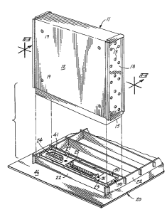
Fig. 1 shows part of an assembled electronic instrument, which
might be any radio frequency testing equipment, such as a signal
generator. The enclosed components of the instrument house circuitry
that includes analog electronic devices -forming circuits that produce
25 radio frequency signals along selected traces in the supporting printed
circuitboards. The assembled circuitry is housed within parallel modular
enclosures 11 that are frictionally attached in perpendicular orientation
to a base circuitboard 20. The base circuitboard 20 includes appropriate
traces to interconnect the modular circuits and devices within a plurality
30 of the parallel enclosures 11.
The invention is not directed to the specifics of the circuitry for
the instruments, but to the physical connecting assemblies for the
electronic and circuitboard components, as well as the shielding elements
provided in conjunction with the housings and the RF signal traces to
35 prevent leakage of radiation to the e~terior of the instrument. In
general, detail~ of the physical structure and specific electronic circuits
and devices mounted on each modular circuitboard 10 is not necessary to
1 3 1 97 4-5
--4--
an understanding of the present system for connecting and shielding
such circuits.
Referring to Figs. 6 and 8, each er.closure 11 houses a modular
circuitboard 10 having an RF circuit mounted to it. The modular
circuitboards 10 are adapted to be arranged in planes perpendicular to
the plane of the base circuitboard 20. They are held in this
perpendicular position by mounting screws 19 attached between the
surrounding enclosure 11 and each interior modular circuitboard 10.
The modular circuitboards 10 and enclosures 11 can be attached to the
base circuitboard 20 or removed from it by hand. This facilitates
assembly, disassembly and repair of the modular components making up
the electronic instrument.
Each modular circuit will include one or more RF signal traces 16
(see Figs. 6 and 8), through which radio frequency signals are directed
between the modular circuitboards 10 by the underlying base
circuitboard 20. Each modular circuitboard 10 will also contain a
continuous ground plane and is provided with various power and control
traces (not shown) that require electrical interconnections through the
base circuitboard 20.
As shown in Figs. 1, 2, 6, 7 and 8, each enclosure 11 is in the
form of a rectangular box including solid continuous metal side walls 12
that are arranged parallel to the interior circuitboard 10. Each
enclosure 11 also includes a bottom opening defined by the lower
extensions of the side walls 12 and bent end walls 15. Walls 12 and 15
together present a continuous peripheral wall configuration about the
bottom enclosure opening that includes interior and exterior wall surfaces
arranged perpendicularly with respect to the plane of the base
circuitboard 20. The intersecting walls 12 and 15 have a configuration
loosely receivable within a socket assembly on- the base circuitboard 20.
3~ They terminate along coplanar bottom edges of enclosure 11.
The interior of each enclosure 11 is ventilated through oppositely
facing end wall assemblies that include double wall baffles comprised of
baffle walls 17 and 18. Environmental ventilation or airflow for cooling
purposes is provided to the interior of enclosure 11 by staggered rows
of apertures 13 formed respectively through the baffle walls 17 and 18.
The patterns for locating the plurality of apertures 13 are selected to
eliminate overlap between the apertures of the two baffle walls 17 and 1~
in planes perpendicular to them. The staggered apertures 13 prevent
131~745
direct escape of radiation from within the interior of enclosure 11 7 while
providing adequate ventilation for dissipating heat produced by the
circuits and devices housed in it. The baffle walls 17 and 18 at each
end of enclosure 11 are slightly spaced from one another and are bent
5 and crimped (as shown in Figs. 7 and 8) to eliminate any physical gaps
through which interior radiation might leak through the open ends 14 in
enclosure 11.
The end walls 17 and 18 form a double-wall cover fixed across end
openings leading to the interior of the box. The perimeter of each
10 opening is defined by the spaced continuous side walls 12 and the
perpendicular top and bottom walls that join them along a continuous
coplanar end edge. Each of the end walls 17 and 18 has a periphery
sealingly engaged about the perimeter of the end box openings. The
first baffle wall 17 has elongated bent edges about its perimeter sealingly
15 engaging the respective walls about the end box opening within which it
is received. The second baffle wall has elongated bent edges about its
perimeter that are doubled baclc upon themselves and sealingly engage
the elongated bent edges of wall 17 and the peripheral walls of the end
opening of the enclosure 11. The bent edges of baffle wall 18 are
20 crimped tightly to secure baffle walls 17 and 18 within each end opening
of the enclosure 11 as a unitary shielding and ventilating structure.
This is illustrated in cross-section in Fig. 8.
The one piece construction of the enclosure 11, in which solid side
walls 12 are also bent to form the enclosure top wall and lower end
25 wall 15, together with the elongated overlapping connections that crimp
the baffle walls 17 and 18 to the enclosure 11 at each of its open ends,
provides radio frequency shielding coverage about the enclosure on five
sides, with no long gaps or cracks through which radiation leakage can
occur. The base circuitboard 20, which has a full top side ground
30 plane 46, forms the sixth side of the circuitboard shield ~see Fig. 6).
This is accomplished by grounding a metal socket assembly on the base
circuitboard 20 to both its top ground plane 46 and its bottom ground
plane 47, as described below, and by sealing the physical connections
between the lower opening of enclosure 11 and the socket assembly by
35 use of a resilient conductive gasket. Leal;age of radiation from belo~Y
the base circuitboard 20 is further prevented by a spaced solid metal
cover 2 8 .
.
1 31 9745
The RF signal connections between each modular circuitboard 10 and
the base circuitboard 20 are provided through a first releasable electrical
connector of conventional design, shown as a multi-pin connector that
includes separable complementary first and second connector elements 31,
5 32. Male connector element 31 is mounted to the upper side of the base
circuitboard 20 and female connector element 32 is mounted to one side of
a modular circuitboard 10 (see Figs. 2 and 6). The illustrated connector
elements 31 and 32, when joined to one another, complete a circuit
between a conductive trace 21 within the base circuitboard 20 and the
10 RF signal trace 16 on the modular circuitboard 10.
While only a single multi-pin connector is shown in the drawings for
conducting RF signals between each modular circuitboard 10 and the base
circuitboard 20, it is to be understood that multiple connectors can be
provided to accommodate the RF signal path requirements of speci~ic
15 circuits included on the modular circuitboards 10.
In the arrangement shown, the male connector element 31 has one
selected conductor or pin 33 electrically connected to the conductive
trace 21 in the base circuitboard 20. The basic electrical connections
are schematically illustrated in Fig. 4, which shows RF signal traces 16
20 on two typical modular circuitboards 10 and a base circuitboard 20. The
five pins 34 adjacent to the selected pin 33 are electricall~J connected to
both ground planes of the base circuitboard by plated-through
connections .
Again referring to Fig. 4, it can be seen that the receiving
25 conductor or socket 36 on the female connector element 32 corresponding
in location to the selected pin 33 of the male connector element 31 is
electrically connected at 35 to the RF signal trace 16 on the modular
circuitboard 10. Similarly, the adjacent five sockets 37 are individually
connected directly to the ground plane by connections schematically at 38
30 and 39. To maintain signal path integrity through the mated connector
elements 31, 32, it is most important that the pins and sockets directly
adjacent to the selected signal pin 33 and receiving socket 36 be
grounded to provide a surrounding grounded environment to the signal
transmitting elements. At least one grounded pin and socket should
35 separate any pins and sockets used for transmission of RF signals
between the modular circuitboards 10 and the base circuitboard 20.
However, where a greater number of pins and sockets are available due
to the economics involved in connector choice, all of the remaining pins
.' ',: ' ~ ' ' ~ .
.
1 31 9745
--7--
and sockets in the connector not used for signal trace communication
purposes may be grounded.
The adjacent grounded pin and socket connections provi~led
alongside the signal pin 33 and socket 36 maintain the integrity of the
5 ground return path for the RF signals as provided on modular
circuitboard 10 by its ground plane in a microstrip structure and on the
base circuitboard 20 by its two ground planes in a stripline structure.
Pin 33 and socket 36 therefore provide an effective interruptible
conductive path between the signal traces on the modular circuitboard 10
10 and the interior of the base circuitboard 20 while maintaining the
integrity of the six-sided shielded enclosure provided about modular
circuitboard 10.
The base circuitboard 20 is conventional in structure. It is a
multi-layer circuitboard having top and bottom outer ground planes 46
15 and ~7 and at least one inner layer of conductive traces. These traces
CRn include power and control signal traces, as well as the exemplary RF
signal trace 21 discussed above.
A grounded metal socket assembly is fi~ed to the base
circuitboard 20 at the full ground plane located at its upper side. It
surrounds the first multi-pin connector and is shown as a series of
intersecting fencc strips 22 spaced about a metal insert 23, as shown in
Figs. 2 and 6. The purpose of the metal socket assembly is to
frictionally mount and support the enclosure 11 that encases each
modular circuitboard 10 and to electrically ground the top ground plane
of the base circuitboard 10 to the modular enclosure 11. The
perpendicular fence strips 22 protrude upwardly from the top ground
plane of base circuitboard 20 (see Fig. 2). Fence strips 22 are slotted
to interlock within one another without any physical gaps through which
radiation might escape. Located immediately inward from each fence
30 strip 22 are similar vertical walls of metal insert 23, which define an
upwardly-open slot surrounding the multi-pin connector.
The socket assembly is completed by yieldable metal spring
gaskets 50, whose cross-sectional configuration is detailed in Fig. 5.
Gaskets 50 are further illustrated in Figs. 3 and 8. Gaskets 50 fit
35 within the upwardly open peripheral slot formed between tlle fence
strips 22 and metal insert 23 for frictionally mounting enclosure 11 to the
base circuitboard 20 with the connector elements 31 and 32 of the
multi-pin connector joined to one another. A physical connection and
'. , ~ `~
' '.
.
131~745
--8-
radio frequency interference seal between each modular circuit assembly
and the base circuitboard 20 is thereby provided by the frictional
interconnections between enclosure 11 and gaskets 50, while the P~F
signal interconnections are provided through multi-pin connectors.
As can be seen in Figs. 3, 5 and 6, the fence strips 22 and
vertical walls of insert 23 are fixed to the base circuitboard 20 by means
of a plurality of closely spaced legs 26 formed integrally along their
lower edges. These legs 26 extend entirely through plated-through
holes in the structure of base circuitboard 20 and are soldered to them
to assure that they are electrically interconnected to both its top and
bottom ground planes 46 and 47. The closely spaced legs 26 effectively
ground the socket assembly to the top ground plane 46 of base
circuitboard 20. They also complete a plurality of electrical connections
between the socket assembly and both ground planes 46 and 47 of base
circuitboard 20 in a shielding pattern within the circuitboard that
surrounds the location of connector element 31.
As can be seen in Figs. 2 and 3, a second multi-pin connector is
prov;ded between each modular circuitboard 10 and the base
circuitboard 20. It also has complementary first and second connector
elements 41, 42 mounted to the top side of the base circuitboard 20 and
to the modular circuitboard 10, respectively. The first or male
connector element 41 and the second or female connector element 42 are
adapted to complete power and control circuits between traces provided
in the base circuitboard 20 and traces on the modular circuitboard 10
(not shown). This second connector is preferably a filtered connector
for direct current power and low frequency control signals. Filtered
connectors capable of preventing passage of RF signals are readily
available for this purpose. In contrast, the RF signal connectors must
be unfiltered so as to not impede the passage of the signals transmitted
through them.
The illustrated metal insert 23 of each socket assembly includes a
base enclosure 24 that separates the connector element 31 and the
connector element 41 at the top ground plane 46 of base circuitboard 20
(see Fig. 2). 3ase enclosure 24 about connector element 41 prevents
radiation within enclosure 11 from coupling onto the control and power
traces at the point where connector element 41 solders to base
circuitboard 20. The base enclosure 24 includes a top wall 27 and an
intermediate transver'se wall 25, whose lower edge has a continuous row
,
1 31 97~5
of legs 26 also extending through plated-through holes in both ground
planes of the base circuitboard 20. Grounding isolation is provided by
legs 26 about corridors extending across the base circuitboard 20 to
confine radiation generated by P~F signal trac~es from coupling onto the
5 power and control lines. The multiple rows of grounded legs 26 for
fence strips 22, inserts 23 and walls 25 at the bottom of the socket
assemblies that mount the removable enclosures 11 to the base
circuitboard 20 also assure that the ground planes 46, 47 at both sides
of base circuitboard 20 are at a constant potential throughout their
10 areas .
As shown schematically in Fig. 4, each conductive trace 21 within
the base circuitboard structure is routed between two parallel rows of
grounded holes or vias 29 formed completely through the base
circuitboard 20 and soldered or plated-through to form electrical
15 connections between its top and bottom ground planes 46, 47. The
grounded vias 29 preferably intersect guard traces 43 extending
alongside the conductive trace 21 to form a coplanar constant-potential
grounded element to confine radiation in trace 21. Since trace 21 is
located between the two full ground planes and the vias and guard
20 traces 43, it is essentially surrounded on all sides by grounded
elements. The result is an electrical connection in the base
circuitboard 20 extending between the various modular circuitboards 10
similar in function to the shielding function of a coaxial cable having a
grounded outer sheath.
The improved shielding characteristics of the present arrangement
are achieved by a complete six-sided grounded enclosure for each
modular circuitboard 10 -- formed by enclosure 24, the socket assembly ,
gaskets 50 and the top ground plane 46. The multi-pin connectors and
conductive traces in base circuitboard 20 provide a shielded electrical
30 connection between the circuits of the modular circuitboards 10 which
pierces this full shield without destroying its integrity. Each RF signal
connection within the base circuitboard is shielded by running between
its top and bottom ground planes 46, 47 and the adjacent rows of
vias 29.
The details of gaskets 50 can best be seen by reference to Figs. 3
and 5. Each gasket 50 is bent from an elongated strip of spring metal
material that is electrically conductive. The RFI shielding gasket 50 is
basically adapted for use within a grounded metal assembly having an
.~
.
' ' .
1 3 1 9745
-10--
open elongated slot of constant cross-section. Such slots are typically
formed by opposed inwardly facing surfaces separated from one another
by a selected spacing. In the illustrated embodiment, the inwardly
facing surfaces are provided between fence strips 22 and the opposing
5 vertical surfaces of metal insert 23. The resulting slot is adapted to
removably receive an elongated edge of a metal wall having a thickness
less than the selected spacing of the slot. Such a wall is illustrated by
the lowermost sections of the side walls 12 and end walls 15 in the
illustrated enclosures 11. The shielding gasket 50 frictionally engages
10 both the surfaces of the slot and the wall received within it.
The formed gasket 50 has a longitudinal bend closing one edge of
the gasket 50. In the illustrated embodiment, this one edge constitutes
the inner edge of the gasket within the slot in which it is used. An
open longitudinal throat is formed at the remaining edge of the folded
15 gasket 50. It includes a pair of opposed, outwardly projecting edges 51
that ar e parallel to one another and to the inner edge of the gasket 50.
The normal maximum transverse width across the edges 51 is greater
than the selected spacing between the inner surfaces of the open slots
formed between fence strips 22 and the opposing vertical walls of metal
20 insert 23. The gasket configuration is completed by a pair of inwardly
bent pinch lines 52 formed in opposition to one another between and
parallel to the outer and inner edges of the gasket 50 within the
receiving slot. The pinch lines 52 are also formed in directions parallel
to the two sharp longitudinal edges 51. The normal transverse spacing
25 between the pinch lines 52 at the interior surfaces of the gasket 50 is
less than the thickness of the metal walls 12 and 15 which are engaged
by the gaslcet 50 when enclosure 11 is mounted to the base
circuitboar d 20.
The outwardly projecting edges 51 at the open longitudinal throat
30 facing upwardly in the open slots of the socket assembly terminate
outwardly along elongated corners formed by intersecting longitudinal
surfaces. This provides a relatively sharp longitudinal corner
configuration at opposite sides of the upper end of each gasket 50 to
insure physical and electrical contact between the sides of the gasket 50
35 and the inwardly facing surfaces of the slot within which it is used.
As seen in Fig. 5, the interior surfaces of the gasket 50 between
its one inner edge and the pinch lines 52 are spaced apart by a
transverse distance greater than the thickness of the metal walls 12 and
: : '
. . .
1 31 97~5
15. This permits the walls 12 and 15 to loosely fit within the folded
gasket 50, with line contact at each side of the walls 12 and 15 being
insured by the resilient gripping action along the pinch lines 52.
Since the gaskets 50 have substantial length, they are slitted at 54
5 ( Fig . 3) periodically along their lengths to relieve uneven bending forces
that might be exerted along a particular gasket 50, thereby permitting
the gaskets 50 to conform more completely to irregularities in the wall
and receiving slot surfaces. Each slit 54 e~tends partially inward from
the throat of the gasket 50 to a location between its folded inner edge
10 and the pinch lines 52 to facilitate resilient adaptation of the gasket 50
to the metal walls 12 and 15 and slot surfaces formed between the fence
strips 22 and the opposed vertical walls of metal insert 23.
As seen in Fig. 5, the gaskets 50 provide a substantial elongated
seal between the open bottom walls of enclosure 11 and the receiving
15 upwardly open slot presented between each fence strip 22 and interior
insert 23 fixed to the base circuitboard 20. There are four lines of
contact between these grounded elements. Referring to Fig. 5, the first
line of contact is indicated by reference numeral 55 and is formed
between one of the top corner edges 51 and the inner surfnce of a fence
20 strip 22. The second line of contact, indicated by reference numeral 56,
is formed along the center of gasket 50 between a pinch line 52 and a
first side of the enclosure wall 12. A third line of contact, indicated by
reference numeral 57, is similarly formed between the opposed pinch
line 52 and the remaining side of wall 12. The fourth line of contact,
25 indicated by reference numeral 58, is presented by the engagement
between the remaining top corner edge 51 along gasket 50 and the
inwardly facing vertical surface of metal insert 23. These four lines of
contact provide multiple insurance against leakage of radiation through
the frictional fittings for each enclosure 11 on the supporting base
30 circuitboard 20. The resiliency of the individual gaskets 50 assures that
these lines of contact will be maintained despite structural variations,
dimensional variations and other irregularities that might be encountered,
since each gasket 50 can shift slightly from one side to the other without
losing good contact along the four lines described.
The gaskets 50 normally remain in place due to their frictional
engagement at the inner surfaces of the upwardly open slots formed
between the metal fence strips 22 and the insert 23. However, when
desired, inwardly facing shoulders can be bent or otherwise formed at
1 31 q745 ~ `
--12-
the top of each slot to retain gaskets 50 when the enclosures 11 are
withdrawn upwardly. Examples of such shoulders are shown by dashed
lines at 59 in Fig. 5.
The invention has been described in language more or less specific
as to structural features. It is to be understood, however, that the
invention is not limited to the specific features shown, since the means
and construction herein disclosed comprise a preferred form of putting
the invention into effect. The invention is, therefore, claimed in any of
10 its forms or modifications within the proper scope of the appended
claims, appropriately interpreted to encompass equivalents.