Language selection

Search

Patent 1319837 Summary

Third-party information liability

Some of the information on this Web page has been provided by external sources. The Government of Canada is not responsible for the accuracy, reliability or currency of the information supplied by external sources. Users wishing to rely upon this information should consult directly with the source of the information. Content provided by external sources is not subject to official languages, privacy and accessibility requirements.

Claims and Abstract availability

Any discrepancies in the text and image of the Claims and Abstract are due to differing posting times. Text of the Claims and Abstract are posted:

  • At the time the application is open to public inspection;
  • At the time of issue of the patent (grant).
(12) Patent: (11) CA 1319837
(21) Application Number: 599946
(54) English Title: INTEGRATED HEATABLE SENSOR
(54) French Title: CAPTEUR A ELEMENT CHAUFFANT INTEGRE
Status: Deemed expired
Bibliographic Data
(52) Canadian Patent Classification (CPC):
  • 73/69
(51) International Patent Classification (IPC):
  • G01N 27/12 (2006.01)
  • G01N 33/00 (2006.01)
(72) Inventors :
  • LEHTO, ARI (Finland)
(73) Owners :
  • VAISALA OY (Finland)
  • NESTE OY (Finland)
  • KEMIRA OY (Finland)
  • OUTOKUMPU OY (Finland)
  • ENGICOM N.V. (Belgium)
(71) Applicants :
(74) Agent: SWABEY OGILVY RENAULT
(74) Associate agent:
(45) Issued: 1993-07-06
(22) Filed Date: 1989-05-17
Availability of licence: N/A
(25) Language of filing: English

Patent Cooperation Treaty (PCT): No

(30) Application Priority Data:
Application No. Country/Territory Date
882697 Finland 1988-06-08

Abstracts

English Abstract


(57) ABSTRACT OF THE DISCLOSURE

The invention concerns a sensor construction for, e.g., the
measurement of gas concentration, comprising a sensor
element (8, 10); a heating element (11) arranged in
conjunction with the sensor, with which the sensor element
can be brought to a temperature above the ambient gas
atmosphere temperature; and an electronics circuitry section
(18), with which the desired electrical properties of the
sensor element (8, 10) can be measured and the heating
element (11) of the sensor (8, 10) can be controlled.
According to the invention, the sensor element (8, 10) and
the electronics circuitry (18) are placed onto the same
planar substrate, and the substrate (1, 7) is processed to
have adjacent openings around the sensor element area (8,
10) to the immediate vicinity of the area so that the
openings (5, 13, 17) extend through the substrate (1, 7),
whereby the sensor area (8, 10) is connected to the
surrounding part of the substrate and, thence, to the
electronics circuitry section (18), only along thin
isthmuses (14) remaining between the openings.

(Figure 1)


Claims

Note: Claims are shown in the official language in which they were submitted.


The embodiments of the invention in which an exclusive
property or privilege is claimed are defined as follows:
1. A sensor for, e.g., the measurement of gas concentration,
comprising

- a sensor element (8, 10),

- a heating element (11) arranged in conjunction
with the sensor for heating the sensor to a
temperature above the ambient gas atmosphere
temperature, and

- an electronics circuitry (18) for the
measurement of the desired electrical properties
of the sensor element (8, 10) as well as for the
control of the heating element (11),

c h a r a c t e r i z e d in that

- the sensor element (8, 10) and the electronics
circuitry (18) are placed on a common planar
substrate, and that

- the substrate (1, 7) is formed with adjacent
openings (5, 13, 17) situated around the sensor
element (8, 10) in the immediate vicinity thereof
and extending through the substrate (1, 7) such
that only thin isthmuses (14) are formed between
the openings (5, 13, 17) for connecting the sensor
element (8, 10) to the surrounding part of the
substrate and, thence, to the electronics
circuitry (18).

2. A sensor construction as claimed in claim 1,
c h a r a c t e r i z e d in that the sensor element (8,
10) and the electronics circuitry section (18) are formed
onto a planar substrate (1, 7) using thick-film techniques.


3. A sensor construction as claimed in claim
1, characterized in that the sensor element (8, 10)
and the electronics circuitry section (18) are
formed onto a planar substrate (1, 7) using thin-
film techniques.

4. A sensor construction as claimed in any
one of claims 1, 2 or 3, characterized in that a
heating resistor (11) of the sensor element (8, 10)
is placed on the bottom surface of the substrate (7)
so as to be aligned with the sensor element (8, 10).

5. A sensor construction as claimed in claim
4, characterized in that the heating resistor (11)
of the sensor element (8, 10) is placed on the top
surface of the substrate (7) so as to be aligned
with the sensor element (8, 10).

6. A sensor construction as claimed in claim
5, characterized in that openings (5, 3, 17) are
processed using a laser.

7. A sensor construction as claimed in claim
6, characterized in that openings (13, 15) are
processed forming two sets of openings, which
coaxially and annularly enclose the sensor element
(8, 10).

8. A sensor construction as claimed in claim
7, characterized in that the sensor element is
attached to the rest of the substrate (1, 7) along
isthmuses by 5 to 15% of its circumference.


9. A sensor construction as claimed in claim
7, characterized in that the sensor element is
attached to the rest of the substrate (1, 7) along
isthmuses by 10% of its circumference.


Description

Note: Descriptions are shown in the official language in which they were submitted.


1 31 9837

Integrated heatable sensor

The present invention relates to an integrated heatable
sensor in accordance with the preamble of claim 1.

Concentration measurements for different types of gases are
performed in an increaslng amount for both the llvlng
envlronment of man and lndustrlal processes. Inflammable
gases can be measured using sensors, whlch are operated with
their surface temperature elevated above the amblent
temperature. Inflammable gases in the ambient air are
thereby oxidized on the sensor surface, and electrons
released in the oxidization process alter the electrical
conductivity of the sensor. Conventlonally, thls change in
sensor resistance is converted lnto a voltage or current,
whose magnitude is proportional to the gas concentration
being measured.

In prior art constructions, the sensors are usually
fabricated as separated sensor elements (or chips), which
are bonded by electrical leads to the case encapsulating the
sensor. In addition, the bonding leads act as springs, which
support the sensor. Another method is to mount the sensor
onto heat-insulating posts, while the electrlcal connectlons
are bonded with thin conductors leads.

The first mentioned construction has two principal
drawbacks. Firstly, the sprlng leads must be deslgned with a
sufficient thickness in order to provide protection for the
sensor against mechanical stresses, e.g., those caused by
lmpact shocks. By contrast, a thlcker lead conducts so much
heat away from the sensor element as to necessitate the
appllcatlon of lncreased heatlng power. Secondly, although
mass production methods are being applied to the processing
of the sensors, their fabrication into separated chips,

.,

131~837
-- 2

individual mounting into the sensor case, and bonding
to the attached electronics, makes the sensor
manufacturing into a complicated and expensive
process.
The aim of the present invention is to
overcome the disadvantages of the abovedescribed
prior art technology and achieve a totally new kind
of integrated heatable sensor.
The invention is based on integrating the
sensor element onto the same substrate with the
electronics circuitry and, further, heat-insulating
it from the rest of the substrate by means of
openings fabricated around the sensor area.
In accordance with a particular embodiment
of the invention there is provided for, a sensor for,
e.g., the meansurement of gas concentration,
comprising:
a sensor element;
a heating element arranged in conjunction
with the sensor for heating the sensor to a
temperature above the ambient gas atmosphere
temperature, and
an electronics circuitry for the
measurement of the desired electrical properties of
the sensor element as well as for the control of the
heating element,
characterized in that,
the sensor element and the electronics
circuitry are placed on a common planar substrate,
and that
the substrate is formed with adjacent
openings situated around the sensor element in the
immediate vicinity thereof and extending through the
substrate such that only thin isthmuses are formed
between the openings for connecting the sensor
element to the surrounding part of the substrate and,
thence, to the electronics circuitry.

1 31 9837
- 2a -

The construction in accordance with the
invention provides outstanding benefits.
The invention makes it possible to
integrate a heatable sensor onto, e.g., the substrate
of a thick-film hybrid circuit so that the sensor and
the substrate form such an integrated structure in
which the heat flow from the sensor to the substrate
is minimized. The sensor can be integrated onto a
substrate containing the electronics circuitry during
a single workphase in the mass production process.
Further, an advantageous method, which is laser
processing, can be applied to the fabrication of the
openings, by virtue of combining this workphase with
that of the thick-film resistor trimming operation
performed during the calibration of the sensors.
The invention is next examined in detail
with help of the following exemplifying embodiments
illustrated in the attached figures.

1 3 t 9837


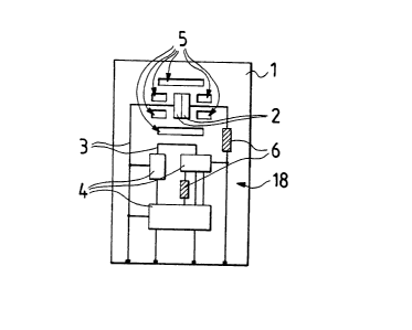
Figure 1 is a top view of an integrated sensor construction
in accordance with the invention.

Figure 2 is a top view of another integrated sensor
construction in accordance with the invention.

Figure 3 is a bottom view of the sensor construction
illustrated in Fig. 2.

With reference to the production methods of thick-film and
thin-film hybrid circuits explicitly described in, e.g.,
such publications as

Hammer D.W., Biggers J.V., Thick Film Hybrid
Microcircuit Technology, Wiley-Interscience 1972,
and

Holmes P.J., Handbook of Thick Film Technology,
Electrochemical Publications Ltd., 1976,

the details of the aforementioned techniques are omitted
herein.

According to Fig. 1, a tin-oxide based sensor 2 is fabri-
cated onto, e.g., an alumina substrate 1 in a conventional
manner, while an additional workphase is also performed by
simultaneously fabricating lead connections 3 of
surface-mount electronical components 4 as well as resistors
6. The heating resistor of the sensor 2 may be placed on
either the lower or the upper surface of the substrate. In
the construction illustrated in the figure, the heating
resistor is placed outside the illustrated area, under the
sensor 2. In con~unction with the bonding of the surface-
mount components 4, openings 5 are fabricated around the
sensor area at appropriate places using, e.g., a laser.
These openings 5 isolate the sensor 2 thermally from the

1 3 1 9837


rest of the substrate. A typical size of the sensor is a few
square millimeters and the size of the substrate is, e.g., 2
* 3 cm2. The width of the cut openings s can be, e.g., a few
hundred micrometers.

In accordance with Fig. 2, metal electrodes 8 and conductors
12 are processed onto a substrate 7 using thick-film or
thin-film techniques. A gas-sensitive layer 10 of
appropriate sensor material, e.g., SnO2 is sintered onto the
electrodes 8. The entity called here a sensor 15 is deflned
to include a sensor materlal layer 10 and the electrodes 8.
In the construction illustrated in the figure, the openings
are arranged so that the sensor 15 is surrounded by an
annular first set of inner openings, consisting of four L-
shaped openings 17, which is further enclosed by a second
set of outer openings, consisting of four rectangular
openings 13. Conductors 12 of the electrodes 8 are routed
via lsthmuses 14 remainlng between the openlngs 13 and 17.
The ratio of the isthmuses to the circumference of the
sensor 15 is about 10 %, but this parameter may be varied
from 5 % to 15 ~ as dictated by the material type and other
needs. The electronic circuitry, together with its
associated components, is not illustrated in the figure;
however, its location is outlined in Fig. 1.

Illustrated in Fig. 3 is the placement of a heating resistor
11 of the sensor to the bottom side of the substrate 7.
Conductors 16 of the heating resistor are routed to the
substrate along isthmuses remaining between openings 13 and
14.

The shape of the openings may obviously vary within very
large limits, since the most advantageous tool, the laser,
offers an extremely wide latitude of control. Hence, the
proposed rectangular shapes of openings can feasibly be
replaced by freely selected shapes with curved contours.

1 3 1 9837


Furthermore, the ideally circular shape can be replaced by
an elliptic contour.

Representative Drawing
A single figure which represents the drawing illustrating the invention.
Administrative Status

For a clearer understanding of the status of the application/patent presented on this page, the site Disclaimer , as well as the definitions for Patent , Administrative Status , Maintenance Fee  and Payment History  should be consulted.

Administrative Status

Title Date
Forecasted Issue Date 1993-07-06
(22) Filed 1989-05-17
(45) Issued 1993-07-06
Deemed Expired 2000-07-06

Abandonment History

There is no abandonment history.

Payment History

Fee Type Anniversary Year Due Date Amount Paid Paid Date
Application Fee $0.00 1989-05-17
Registration of a document - section 124 $0.00 1989-09-06
Maintenance Fee - Patent - Old Act 2 1995-07-06 $100.00 1995-06-14
Maintenance Fee - Patent - Old Act 3 1996-07-08 $100.00 1996-06-26
Maintenance Fee - Patent - Old Act 4 1997-07-07 $100.00 1997-06-10
Maintenance Fee - Patent - Old Act 5 1998-07-06 $150.00 1998-06-17
Owners on Record

Note: Records showing the ownership history in alphabetical order.

Current Owners on Record
VAISALA OY
NESTE OY
KEMIRA OY
OUTOKUMPU OY
ENGICOM N.V.
Past Owners on Record
LEHTO, ARI
Past Owners that do not appear in the "Owners on Record" listing will appear in other documentation within the application.
Documents

To view selected files, please enter reCAPTCHA code :


To view images, click a link in the Document Description column. To download the documents, select one or more checkboxes in the first column and then click the "Download Selected in PDF format (Zip Archive)" or the "Download Selected as Single PDF" button.

List of published and non-published patent-specific documents on the CPD .

If you have any difficulty accessing content, you can call the Client Service Centre at 1-866-997-1936 or send them an e-mail at CIPO Client Service Centre.


Document
Description 
Date
(yyyy-mm-dd) 
Number of pages   Size of Image (KB) 
Drawings 1993-11-17 2 32
Claims 1993-11-17 3 63
Abstract 1993-11-17 1 26
Cover Page 1993-11-17 1 12
Description 1993-11-17 6 177
Representative Drawing 2002-05-01 1 5
PCT Correspondence 1993-04-19 1 32
Prosecution Correspondence 1993-01-13 2 48
Examiner Requisition 1992-09-25 1 65
Prosecution Correspondence 1992-07-07 2 63
Examiner Requisition 1992-03-16 1 68
Fees 1996-06-26 1 48
Fees 1995-06-14 1 49