Note: Descriptions are shown in the official language in which they were submitted.
- l - 1319~7
This invention relates to a frequency synthesizer
especially but not exclusively for use in a digital wireless
telephone system wherein a subscriber unit is adapted to be
in wireless connection with a base station. The subscriber
unit has a baseband processor which performs a number of
functions including the transcoding of incoming and outgoing
signals from one type of bit stream to another and the
provision of echo cancellation. It also acts as a control
microprocessor such as, for example, by informing a
synthesizer in the system as to the desired operational
frequency to be used. It is, in addition, coupled to storage
means for receiving and storing the various functions
performed or received thereby.
The baseband processor is connected to a modem
processor to which it is coupled by a direct access means
that prevents simultaneous access by both of these
processors, but the two processors do communicate with each
other, and the modem processor, which acts as the master in
the system, may access the baseband processor's memory
through the direct access means. However, lock-out means are
provided whereby, in certain circumstances, control of the
baseband proce,sor by the modem processor is prevented.
The modem processor sends its signals, at a
predetermined sampling rate, through a frequency translated
complex signal which is converted to an analog signal. This
analog signal is subjected to deglitching by means of a
blanking process. The deglitched signal is then upconverted
and filtered to form an IF signal which is thereafter
amplified. The frequency of the amplified IF signal is added
to a frequer~y generated by the aforesaid synthesizer and the
resultant RF slgnal is amplified and passed to an antenna.
The subscriber unit utilizes contin~10~sly repetitive
frames in which it transmits during one portion of each frame
and receives during another portion thereof, these portions
being designated "slots". On the basis of certain signals
received from the base station, the baseband processor
- 2 - i3 ~9~ ~
produces initiating signals which determine whPther the
subscriber unit will be in the transmit mode or the receive
mode.
In intervals between actuation of the system, a
training mode is used wherein a known signal from the modem
processor is compared with a looped-back signal to produce
correction constants to compensate for undesirable variations
in the IF signal due to variations in temperature, component
values, etc. are obtained. These correction constants are
stored for use in correcting actual received signals.
During the demodulation, the modulated digital
signals are fed to the modem processor in the form of time
multiplexed I and Q samples and are demultiplexed. The
demultiplexed I and Q samples are fed to an equalizer and
frequency correction circuit for minimization of errors,
resulting in the production of frequency correction signals
which are used to correct any errors in the timing of the
system and in the output of the synthesizer.
According to the invention, there is provided a
frequency synthesizer for converting an IF signal to a signal
of a predetermined assigned frequency comprising a frequency
synthesizer having a pair of outputs wherein a first output
is offset from a second output by a predetermined frequency,
said first output acting to generate a frequency which, when
combined with the frequency of the IF signal, provides a
signal of a predetermined desired frequency, and said second
output being combined with a received signal to produce a
signal having the same frequency as said IF signal.
~RIEF DESCRIPTION OF THE DRAWINGS
Figure 1 is a diagrammatic view showing a Subscriber
unit embodying the present invention.
Figure 2 is a block diagram of the modulator portion
of the modem processor shown in Figure 1.
_ 3 _
Figure 3 is a block diagram of the DPSK conversion
unit shown in Figure 2.
Figure 4 illustrates the structure and function of
the FIR filter shown in Figure 2.
Figure 5 is a block diagram of the interpolator shown
in Figure 1.
Figure 6 is a block diagram of the synthesizer shown
in Figure 1.
Figllre 7 is a modified form of the input portion of
the system shown in Figure 1.
Figure 8 is a block diagram of the demodulator
portion of the modem processor shown in Figure 1.
Figure 9 is a block diagram of the course frequency
control module shown in Figure 8.
Figure 10 is a block diagram of the AFC and symbol
timing module shown in Figure 8.
GLOSSARY
Glossary of acronyms and words used in the Specification
ACRONYM DEFINITION
20 A/D Analog-to-Digital Converter
ADJ Adjustment Input
AFC Automatic Frequency Control
AGC Automatic Gain Control
BLANKING Control means for causing a signal to be
held at a predetermined amplitude level
during actuation of the control means
CODEC Combined Coder and Decoder
CPE Customer Provided Equipment (telephone
instrument)
30 D/A Digital-to-Analog Converter
DMA Direct Memory Access
DPSK Differential Phase Shift Keving Modulation
DS Data Select
EEPROM Electrically Erasable Programable Read
Only Memory
~3199i~
-- 4
EPROM Erasable Programable Read Only Memory
FIFO First-In First-Out Memory
FIR Finite Impulse Response
GLITCH Undesired Transient Signal
5 HOLD Idle Mode
I In-Phase
IF Intermediate Frequency
Kbps Kilobits per second
nS Nanosecond
10 PAL Programable Array Logic
PCM Pulse Code Modulation
PROM Programable Read Only Memory
PSK Phase Shift Keying Modulation
Q Quadrature
15 RAM Random Access Memory
RELP Residual Excited Linear Prediction
RF Radio Frequency
R/W Read/Write
S/H Sample and Hold
20 SLIC Subscriber Loop Interface Circuit
STROBE Sampling Signal
UA~T Universal Asynchronous Receiver Transmitter
VCXO Voltage Controlled Crystal Oscillator
XF External Flag Output Used for Signalling
Other Processors
SPECIFICATION
This invention relates to communications systems for
the wireless transmission of multiple information signals
utilizing digital time division circuits between a base
station and one or more subscriber stations, and it
particularly relates to the structure and functioning of such
a subscriber station.
Referring now in greater detail to the drawings
wherein similar reference characters refer to similar parts,
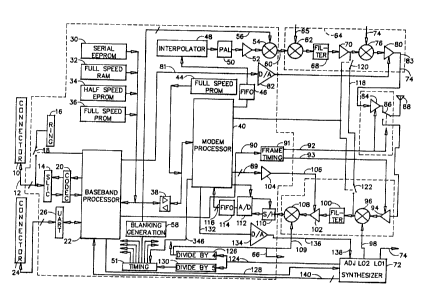
there is shown in Figure 1 a connector 10 for connection to
- 5 - ~ 9 ~ ~ ~
the customer-provided equipment (CPE). A line pair 12 leads
from the connector 10 to a SLIC 14 and is also connectable to
a ringer circuit 16 through a relay 18. The SLIC 14 is a
standard chip for providing various functions such as battery
voltage, over-voltage production, ringing, signalling
detection, as from a rotary dial, the handset status, line
testing, etc. It also contains the hybrid which separates a
plurality of voices into ingoing and outgoing signals. The
SLIC 14 is ~oupled to a codec 20 having ingoing and outgoing
lines to and from a baseband processor 22 whereby in the
ingoing direction it converts analog voice signals to digital
signals, i.e., 64 kbps u-law PCM, while in the outgoing
direction, it converts the digital signals to analog voice
signals. It may sometimes be desirable to bypass the codec
so that the SLIC 14 is directly coupled to the baseband
processor 22. There is an alternative access to the baseband
processor through a connector 24 and a IJART 26, which
provides a direct digital connection to the baseband
processor, thereby bypassing the SLIC and codec. This direct
access connection serves two purposes: (1) to pass only
digital signals, when so desired, thereby bypassing all
analog connections, and (2) to allow direct access to the
processors and memories for easy maintenance and test
purposes.
The baseband processor 22 has several functions, one
of which is to convert the 64 kbps PCM signal to 14.57..~
kbps by means of a transcodinq function, which as, for
example, provided by residual excited linear prediction
(RELP). It also provides echo cancellation, and, in
addition, acts like a control microprocessor, as, for
example, by informing the synthesizer used in the system as
to the desired operational frequency. The baseband processor
22 is coupled to a bootstrap memory chip 28 as well as to a
serial EEPROM 30, which is an electrically erasable, non-
volatile memory where selected bits may be electricallyerased without erasing other bits stored therein. This
- 6 - ~ 3~ ~9 ~ 7
EEPROM 30 is used to store both the subscriber identification
number and the network identification number (the base
station with which it is used). In addition, the baseband
processor 2~ is coupled to a full speed RAM 32 in which it
stores the signals received therein. The RAM 32 also
includes a "cache" means, and, in addition, is used as a
random access memory for RELP conversion, echo cancellation
and other control functions. The baseband processor 22 is
also coupled to a half-speed EPROM 34 and a full-speed PROM
36 which store the RELP and echo cancellation functions as
well as various other functions such as the control function.
The baseband processor 22 is, in addition, coupled via direct
memory access (DMA) 38 to a modem processor 40.
The DMA 38 prevents the occurrence of simultaneous
access of RAM 32 by both the baseband and modem processors.
The DMA interface is used to transfer voice and
control data between the baseband ànd modem processors. The
modem processor 40 acts as the master and controls the
baseband processor 22 via hold lines (not shown). The modem
processor 40 has the capability to access the baseband
processor 22, halt its processing and cause the control
lines, address and the data busses to assume the high
impedance state of a three-state output. This permits the
modem processor 40 to access the baseband processor's DMA
memory through the DMA Interface and read or write to it.
This is accomplished by the modem processor 40
asserting its XF bit, which is gated to the baseband
processor's Hold input. When the baseband processor receives
this command, it will finish executing the current
instruction, stop its processing, cause its control data and
address busces to assume the high impedance state of a three-
state output and then issue a Hold Acknowledye signal back to
the modem processor. Immediately after the modem processor
issues the Hold command, it will continue on with other tasks
while waiting for the baseband processor to send the Hold
Acknowledge signal. Once the modem processor receives the
_ 7 _ ~3~9~37
Hold Acknowledge signal, it will take control of the baseband
processor's control, data, and address buses and then read or
write to the DMA RAM 32. After the modem processor completes
accessing the DMA RAM, it will take away the Hold input on
the baseband processor, which will then resume processing
where it left off. The baseband processor also has the
capability to lock out the modem processor by setting its own
XF bit high. This bit is gated with the Hold from the modem
processor and can override the Hold line at any point before
the baseband processor goes into the Hold state. The modem
processor uses 10 bits of the address bus and all 16 bits of
the data bus. It also uses three control lines: Strobe,
R/W, and DS.
Either the baseband processor 22 or the modem
processor 40, acting in either direction, may obtain signals
from the RAM 32 in accordance with the signals described
above. The two processors communicate with each other by way
of a portion of RAM 32 that is set aside to be used as a
cache. The modem processor 40 is also coupled to a full
speed PROM 44 which contains the program for this processor.
The modem processor 40, in its modulation mode, sends
its signals via a FIFO 46 to an interpolator 48, these
signals being at a sampling rate of 320 kHz. The
interpolator 48 effectively increases this sampling rate by
5 to convert it to 1600 kilosamples~second (1.6
megasamples/second). The interpolator, in conjunction with
the crystal filter (hereinafter described), which acts as an
integrator, effectively approximates a 5 tap FIR filter.
This usage of digital and analog hardware to implement an FIR
filter differs from the classic all digital hardware FIR
~mplementation. The interpolator output is fed into a PAL
50.
The PAL is configured as a type of mixer into which
is fed a 400 kHz square wave, as indicated at 50, which comes
from a timing generator 51, as we~i as the 1600
kilosamples/second signal. The 1600 kilosamples/second
- 8 - 1~ 7
signal represents a 16-kilosymbol/second PSK signal with a
zero carrier and a desired 20 kHz bandwidth. In effect, the
PAL can be considered as a frequency translator. The PAL
circuit which when configured to perform a 2's complement
function controlled by a 400 kHz square wave effectively
performs a time multiplexed quadrature mixing and effectively
translates the 20 kHz wide baseband signal up to 400 kHz.
The output from the PAL 50 is a time multiplexed,
frequency translated complex signal which is passed to the
D/A converter 52 which converts the digital signal into an
analog signal. The output from the D/A converter 52 is fed
to a mixer 54 into which is also fed a deglitching/blanking
pulse 56 from a blanking generation module 58. Glitch energy
is a major contribution to noise in a sampled data system.
Glitch energy occurs during transitions from one input word
to another. In a D/A converter, each incoming bit, depending
upon its state, may cause a change in output analog level.
Such changes resulting from the various bits usually do not
occur simultaneously and therefore cause glitches. Classical
solutions to this problem are the use of a sample and hold
following the D/A or the use of a de-glitching D/A. Both of
these alternatives, however, are unduly expensive.
"Blanking" returns the output of the mixer to an intermediate
reference level during the transition periods, typically
about 35 nS before and 130 nS after the digital switching
times, thereby suppressing large glitch spikes that occur on
the D/A output. Although blanking creates harmonics away
from the center fre~uency of interest, the use of relatively
tight IF filtering substantially removes these harmonics.
This blanking method also reduces the sampling rate content
in the output.
The output from mixer 54, indicated at 60, is fed to
a mixer 62 in an upconverter, generally designated 64. The
mixer 62 has a 20 MHz input indicated at 65, which is common
with a 20 M~z line 66. The output of mixer 62 is the sum of
20 MHz fro~ input 65 and the 400 kHz signal received from
- 9 - 13~9~7
mixer 54, with a resultant output of 20.4 MHz. This output
is fed into a crystal filter 68 which passes only this sum,
constituting the IF signal, to an amplifier 70.
A synthesizer is shown at 72. Within this
synthesizer 72 is a synthesizer module which provides an
output LOl. Also within the synthesizer module, a second
circuit derives a second output LO2 wherein the output of LO2
tracks the output of LOl at a fre~uency of 5 MHz below the
frequency of LOl. The synthesizer uses as a reference the 80
MHz VCXO. The output LOl is fed through line 74 to a mixer
76 which also receives the IF output from amplifier 70.
Since the IF signal has a value of 20.4 MHz, if, for example,
a frequency of 455.5 MHz is desired at the output of mixer
76, the synthesizer is operated to generate a frequency of
435.1 MHz, which when added to the 20.4 MHz, gives the
desired frequency of 455.5 MHz. This output is then
amplified by a variable gain amplifier 80. The baseband
processor 22, on the basis of decoding certain signals from
the base station, sends a gain control signal on line 81,
through a D/A converter 82, to the variable gain amplifier
80. Variable gain amplifier 80 has limited bandwidth and,
therefore, does not pass the undesired difference frequency
also produced by the mixer 76. The output of amplifier 80 is
passed through line 83 to a power amplifier 84, which
accomplishes the final amplification before the RF signal
passes through a relay 86 to an antenna 88.
The unit employs a system whereby a frame repeats
every 45 milliseconds. In this system, the unit transmits
during a portion of the second half of each frame and
receives during a portion of the first half of the frame.
One configuration might be where both portions of the half
are of equal length (although they may not necessarily be
equal). Another configuration (16-ary) might be where four
e~ual length portions are available to the subscriber during
an entire frame. Each of the four portions may be termed a
slot. Each slot contains, as part of its initial data, a
- lo 1~ 7
unique word which is used by the unit to establish timing for
reception of the remaining data in the slot. The first slot
of the four is preceded by an AM hole which is used to
determine a slot arbitrarily designated by the base station
as the first slot. The AM hole and the unique word are part
of the incoming signal from the base station. The duration
of the AM hole is used to determine whether a particular RF
channel is a control channel or a voice channel.
A data signal is derived from the average magnitude
of the signal represented at 116. A threshold proportional
to said average magnitude is compared to unaveraged
magnitudes. If the threshold is not exceeded by said
unaveraged magnitude for a predetermined period of time, it
is assumed that an AM hole has been detected. The modem
processor 40 stores the time at which the AM hole was
determined to occur in RAM 32. The baseband processor, on
the basis of (a) modulation mode (4-ary or 16-ary), (b) the
time at which an AM hole occurred, as stored in RAM 32, and
(c) the time at which a unique word was received, as
separately determined by the baseband processor, produces
initiating signals which indicate when the unit should be in
a transmit mode or a receive mode. Such initiating signals
are coupled via line 90 to frame timing module 91.
The frame timing module 91 converts the initiating
signals into two series of pulses. One series of pulses is
connected via line 92 to enable power amplifier 84 and to
actuate relay 86 so as to connect the output of amplifier 84
to antenna 88. During the period of the pulse on line 92,
the unit i~ designated to be in the transmit mode. When
relay 86 is not so actuated, it is configured to connect
antenna 88 to the input of preamplifier 94.
The other series of pulses from frame timing module
91 are connected via line 93 to a preamplifier 94 to enable
this preamplifier. The unit is designated to be in the
receive mode during this series of pulses. The preamplifier
94 passes received signals to a mixer 96, which also receives
output L02 from the synthesizer 72 through line 98~ The
output of mixer 96 is fed to a crystal filter 100, the output
of which, in turn, is fed to an IF amplifier 102.
The modem processor 40 passes via line 89, the
aforementioned data signal, which is derived from the average
magnitude of the signal represented at 116, to a D/A
converter 104 which produces an analog AGC voltage signal
which passes through line 106 to amplifier 102, thereby
indicating to this amplifier how much gain is required in
order to compensate so that the IF signal is always at the
same amplitude. This amplifier also receives the output from
crystal filter 100. The output from amplifier 102 passes to
a mixer 108 into which is also applied an input of 200 kHz
from line 109 to produce a resultant 400 MHz signal. This
400 kHz signal is then passed to an A/D module which consists
of sample and hold circuits 110, and A/D converter 112 and a
FIF0 114.
The output from the A/D conversion module is 64
kilosamples/second and this output is fed through line 116
into the modem processor 40. The modem processor 40
demodulates this signal and passes the demodulated data into
the cache portion of RAM 32 which is accessed by the baseband
processor 22 in which the RELP conversion takes place. The
resultant output has 64 kbps PCM on a continuous serial
basis. This output is fed to the codec, which converts it to
an analog signal that is then fed to the SLIC which, in turn,
feeds it to the telephone instrument; or, alternatively, the
16 kbps fro~ the cache can be decoded into a digital signal
which is fed to the UART 26.
When used in the training mode, a loopback is
provided at 118 between two relays 120 and 122. This
loopback, which is at the IF side rather than at the RF side,
decreases the number of elements required. The training mode
is that in which a known signal is sent out by the modem
processor through the remainder of the transmitter elements
~3i~g~7
- 12 -
set to IF amplifier 70. Because relays 120 and 122 are
operated, the output of the amplifier 70 is connected to the
input of crystal filter 100.
Additionally, an output of the baseband processor 22,
indicated line 90, fuses to frame timing 91 and causes a
pulse on line 93 to totally disable amplifier 94 during the
training mode. Furthermore, during the training mode, frame
timing 91 produces another pulse on line 92 which totally
disables amplifier 84. The known signal generated by the
lo modulator is compared with the actual signal returned to the
demodulator. A subsidiary program is then set up to
compensate for variations due to various factors such as
variations in temperature, component values, etc. The
correction constants are stored in the RAM 32. The modem
applies these stored corrections to the received signals.
The training mode takes place in intervals between actuation
of the system.
The synthesizer module 72 contains an gO MHz
oscillator (VCX0) derived from the received signal. The 80
MHz signal generated by the oscillator goes through line 124
to a divide-by-4 circuit 126, the output of which goes to
mixers 62 and 108. This output also goes to the two
processors to provide clock pulses (square waves). In
addition, it goes through line 124 to a divide-by-S circuit
130 and then to timing module 51. The modem processor
determines any difference in frequency between the center
frequency of the input signal and a submultiple of the clock
frequency.
Any resulting difference is applied by the modem
processor, via line 132, to a D~A converter 134. The output
of the D/A converter 134 is applied via line 136 and ADJ
input 138 to the VCX0 (hereinafter described) in such a
manner as to change its frequency in the direction required
to minimize the preceding resulting difference. A lock loss
detector signaL is applied through line 14C to the baseband
- 13 - ~ 7
processor 22 to indicate when there is a loss of
synchronization in the synthesizer.
The modem processor 40, as shown in Figure 2,
comprises a DPSK converter 150 into which data is fed through
line 152. The data is then fed at 16 kHz symbol/second rate,
to a FIR filter 154. The output from FIR filter lS4,
indicated at 156, is asynchronous data comprising 10 complex
samples/symbol, time-multiplexed IQ pairs. This output is
fed to the ~IFO 46, described above, where asynchronous to
synchronous conversion takes place. The output from the FIFO
46, in the form of 160,000 pairs of data words/second, is fed
into the interpolator 48, described above, which
demultiplexes the IQ pairs, and remultiplexes the IQ samples
at 1.6 MHz rate.
In a 16-ary modulation scheme, the binary input
sequence is divided up into 4-bit symbols. In 16-ary PSK,
the 4-bit symbols determine the phase of the carrier during
the given symbol period. The task of converting the binary
input to the PSK waveform is performed by the modulator.
Figure 3 shows how a sequence of sa.nples (S), shown
at 160, is transformed into a sequence of Inphase (I) and
Quadrature (Q) samples in the DPSK converter 150 of the modem
processor 4t!. The symbols are first inverse Gray encoded, as
shown at 16~. This is done to minimize the number of bit
errors that occur due to the most likely incorrect symbol
decisions in the demodulator.
The output of the inverse Gray encoder 162 is fed
into a pha~e quantizer 164 which determines the absolute
phase value O, introduced by the current symbol. This phase
value is then fed into the differential encoded 166 which
computes the absolute phase value O;'. O;' represents the
modulo 16 sum of the current differential phase O, and the
previous phase O;-/'.
~ + ~ -/ ') MOD 16
The modulo 16 addition corresponds to the modulo 360
addition th~t is performed when adding angles.
~ 3 ~
The differential phase ~j' is fed into cos and sin
lookup tables to compute the I and Q components of the
current symbol.
The I and Q samples are fed into the 6-tap Finite
Impulse Response (FI~) filter 154 shown more specifically in
Figure 4. The function of the FIR filter is to create an
oversampled PSK waveform from the I and Q samples. The Q
samples are fed into a bank of ten 6-tap FIR filters labelled
"hj,j" (j = 1 through 10). Similarly, the I samples are fed
into a bank o ten filters labelled llhajll. The outputs of
these 20 filters are time division multiplexed as shown onto
a single parallel bus that runs at a sampling rate which is
ten times the sampling rate of the I,Q pairs at the input of
the filter.
The interpolator 48, shown more specifically in
Figure 5, comprises an input 180 and a relay 182 that is
connected to the PAL 50 by a line 183, the relay 182 being
movable between the input 180 and a line 184. Optionally
insertable in the line 183 is a multiplier la5 that may be
used to multiply the inputs from the line 183 as well as an
optional input 187 that may be applied from the modem
processor or from any desired auxiliary memory. The relay
182 is connected to the PAL 50 by the line 183 and the line
184 leads from the I memory 186 which has an input 188 from
the Q memory 190. A 1.6 MHz input is provided for both the
I/Q and ~/I memories as indicated at 192 and 194
respectively. ~he interpolator demultiplexe~ the multiplexed
I.Q samples at a 160 kHz rate and then resamples and
remultiplexes at an 800 kHz rate.
The synthesizer 72, functionally described above, is
illustrated in Figure 6, where there is shown an 80 MHz VCXO
module 200 that receives a signal from the ADJ input 138.
This input controls the exact frequency of the VCXO module.
The output from the VCXO module is connected via line 202 to
the synthesizer 204. This synthesizer 2G4 is capable of
synthesizin~ frequencies between 438.625 and 439.65 MHz in
- 15 -
appropriate synchronism with the signals over line 202. The
particular frequency is selected by an input signal over line
128 (also shown in Figure 1).
The output of the synthesizer 204 is fed, via line
206 and filter 208 to become L01. The output of synthesizer
204 is also fed, via line 210, to a synchronous translator
212. The output of the VCX0 200 is fed through line 214 to
a divide by 16 module 216, the 5 MHz output of which is fed
through line 218 to the synchronous translator module 212.
The output on line 214 is also connect~d to a reference
output 221.
Module 212 subtracts the 6 MHz input from line 218
from the frequency on line 210, producing a difference
frequency that is fed, via filter 220, to become Lo2. In
this manner, the frequencies appearing as L02 vary between
433.625 and 434.65 MHz, whereby the frequency of the L02 is
always 5 MHz below the frequency of L01.
Additionally, the output from the synthesizer 204,
via line 222, and the output from the synchronous translator
212, via li~e 224, are combined in a synchronization detector
226 in such manner that if either the frequency on line 206
is not synchronous with the frequency on line 202 or the
frequency output of synchronous translator 212 is not
synchronous with the combination of the frequency on line 206
and the output frequency of the divide-by-:!6 module 216, a
loss of synchronization (lock loss) signal is sent on line
140 (also shown in Figure 1.).
The particular combination of one synthesizer 204
plus the divide-by-16 module 216 and che synchronous
translator 212 provides the same function as the two separate
synthesizers previously used, but with fewer parts, greater
stability, easier tolerances, etc.
~ igure 7 illustrates a preferred circuit to test the
customer interface. In this respect, the modem processor 22
(shown in Figure 1) digitally generates a 1 kHz sine wave
that is passed to the codec 20 (shown in Figure 1) that
~3~9~7
- 16 -
converts it to an analog sine wave which is, in turn, passed
through the hybrid function of the SLIC 14 to line pair 12.
A relay K (not shown in Figure 1) is inserted immediately
adjacent the connector 10 so that it may disconnect the
connector from the circuit. Any reflected signal from the
unterminated line pair 12 at the open relay K is returned
through the hybrid function of the SLIC and is converted to
a digital signal by the codec 20. This digital signal is fed
to the baseband processor 22 which compares the reflected
signal with the originating signal and determines whether any
undesired impedances or connections, e.g. grounds, are
present on the line pair 12.
Figure 8 illustrates the demodulator portion of the
modem processor 40 and shows the 400 kHz output from the
mixer 108 (shown in Figure 1) applied to the high precision
sample and hold circuit 110, which has an aperture
uncertainty of 25 nanoseconds or less, the output of which is
passed to the A/D converter 112. The output of A/D converter
112 is fed through line 116 to the modem processor (all as
shown in Figure 1). The input at line 116 comprises time
multiplexed I and Q samples (which may have some cross-
product distortion) in the form of two complex sample
pairs/symbol. Said time multiplexed I and Q samples are
applied to the demultiplexer 298 where they are
demultiplexed. The demultiplexed I and Q samples are applied
to an equalizer module 300 whose objectives are to minimize
(a) error energy of the received data stream, (b) modified
error energy of the data stream delayed by 0.05 T (T being
1/16000 of a second), (c) modified error energy of the data
stream advanced by 0.05 T, (d) energy of the data stream from
the adjacent upper channel (desired receive frequency plus 25
kHz), and (e) energy from the data stream of the adjacent
lower channel (desired receive frequency minus 25 kHz).
The equalizer is a complex 28 tap FIR filter wherein
the filter weights are determined by minimizing the above
five object:ives. For this purpose, five training signals are
131~7
- 17 -
generated by the modulator. These are: (a~ a signal at the
desired frequency wherein the receiver and transmitter clocks
are synchronized, (b) the same signal as (a) but wherein the
receiver clock is advanced with respect to the transmitter
clock by 0.05 T, (c) the same signal as (b) except that it is
delayed by 0.05 T, (d) the same signal as (a) but wherein the
carrier frequency is increased by 25 kHz, and (e) the same
signal as (d) except that the carrier frequency is decreased
by 25 kHz. In cases (d) and (e), to create the training
signal with a 25 kHz deviation, the modem processor shifts
the transmit FIR filter coefficients by 25 kHz.
By comparing the actual inputs during the
presentations of each of the five training signals with a set
of desired outputs, a set of weighting coefficients is
obtained, which when implemented in the equalizer, achieve
the aforementioned objectives. These weighting coefficients
- are stored in the RAM 32.
The equalized I and Q samples are fed into a module
302 which produces an output which is the arc tangent of the
ratio ~f the equalized Q and I samples. This output, shown
at 304, rep:resents the phase of the received signal.
The equalized I and Q samples are al;~ simultaneously
fed to a course frequency module 306, shown in greater detail
in Figure 9. The I and Q samples are summed to produce a
lower sideband 308 (as shown in Figure 9), and simultaneously
the difference between the I and Q samples is formed to
produce an upper sideband 310. A magnitude calculation is
then performed on both the upper and lower sidebands, as
indicated at 312 and 314. The difference operation between
the magnitudes take place at 316. This difference indicated
at 318, represents a frequency error.
As shown in Figure 8, the output 304 of the arc
tangent modu'e 302 is fed to the AFC and symbol time tracking
module 320 (which is shown in greater detai.! in Figure 10).
35 The phase correction value, indicated at 322 in Figure 10, is
subtracted from the detected phase 304, resulting in the
~31~7
- lS -
corrected phase indicated at line 324~ The corrected phase
324 is fed into a symbol detector 326 which detects the
current symbol in terms of the phase value and quantizes the
phase to the nearest 22.5 degree increment. The quantized
phase, indicated at 328, is subtracted from the corrected
phase 324 at 330. This results in the phase error signal
indicated at 332. This error signal 332 is fed into a second
order loop filter, generally indicated at 334, which computes
the phase correction value, indicated at line 336, as well as
the frequency correction signal, shown at 338. This
frequency correction signal is applied to the VCXO through
line 132 shown in Figure 1.
The error signal 332 is fed through line 340 to a
symbol timing tracking module 342 which also receives the
output from the symbol detection module 326 through line 344.
The symbol timing tracking module 342 contains an algorithm
which tracks the phase over a number of predetermined
symbols, looking at the starting phase of the first symbol
and the phase of the last symbol, and then determines the
slope. It tries to determine from the phase versus time
function where the zero crossings that actually occurred and
comparing them with where they should have occurred, a timing
adjustment is computed that will correct for the difference.
The symbol clock will be adjusted at the beginning of the
next slot. The symbol timing tracking module 342 provides an
output 346 which is applied to the timing module 51 (shown in
Figure 1).
The frequency correction signal 338 from the AFC and
symbol timing module 320 is applied to a weighting module 348
(as shown in Figure 8) where it is weighted. The output 350
from module 348 is fed into a summing module 352 where signal
350 is summed with the output 318 of module ~06 to provide an
output 354 which is applled to the D/A converter 134. The
output lrom D/A converter is shown in Figure 1 as being
applied to the synthesizer at 138.
- 19 -
Although the invention, as described above, provides
for various separate elements, it is possib~e to include the
functions of many of these elements such as, for example, the
full speed PROM 44, the FIFO 46, the interpolator 48 and the
PAL 50, within a modem processor of sufficiently large
capacity. This may also be true of such elements as the
frame timing 91, the blanking generation 58, the timing means
Sl, the divide-by-4, the divide-by-5 and some or all of the
synthesizer 72. Furthermore, the baseband processor and the
1~ modem processor may also be combined in a simple unit which
may also incluc1e the codec and the UART.