Note: Descriptions are shown in the official language in which they were submitted.
~ 3 ~
Magneto-optical recording apparatus and energizing circuit
for use in such a magneto-optical recording apparatus.
The invention relates to a magneto-optical
recording apparatus for recording an information signal on
a magneto-optical record carrier, which recording apparatus
comprises a field coil for generating a magnetic field in
the record carrier, an energizing circuit for energizing
the field coil, and a control circuit for controlling the
energizing circuit depending on the information signal in
order to modulate the generated magnetic field in conformity
with the information signal.
The invention further relates to an energizing
circuit for use in such a magneto-optical recording appara-
tus.
For recording in magneto-optical materials it was
customary until now to magnetise the magneto-optical
15 material in a specific direction prior to recording and
subsequently during recording to expose the material to a
magnetic field whose direction is opposite to the direction
of the previously applied magnetization and at the same
time to heat the material locally by means of an intensity-
20 modulated laser beam to a temperature near the Curie point,to produce a pattern of magnetic domains corresponding to
the modulation pattern and having a direction of magneti-
zation which differs from the surrounding area.
This method has the drawback that the previously
2~ recorded part must be erased before a new recording can
be made.
A recording technique which mitigates this draw-
back is already known from Philips Technical Review, Vol.
42, no. 2, August 1985, page 41. In this recording technique
30 the magnetic field is modulated instead of the laser beam.
However, this recording technique using magnetic-field
modulation is not utilised in practice because no satis-
2 1~38~
factory solution has been found for the circuit for energi-
zing the field coil. The problem then encountered is that
as a result of the strong magnetic field (approximately
200-300 oersted) the energy stored in the magnetic field
5 is so high that the magnetic field can only be reversed
rapidly enough by applying a large voltage difference
across the magnetic coil, which in principle can be realised
by means of voltage sources having a high output voltage
(approximately 100 V). The field coil can then be energized
10 via a series resistor to limit the steady-state current.
In conventional magneto-optical recording apparatuses, in
which the remainder of the electronic circuitry operates
with a supply voltage of 5-15 V, magnetic-field modulation
therefore means that an additional 100-V voltage source has
5 to be used, which makes magneto-optical recording with a
modulated magnetic field impracticable, the use of the
series resistor has the disadvantage that a substantial
amount of heat (approximately 10 W) is dissipated in the
series resistor.
It is the object of the invention to provide a
magneto-optical recording apparatus which requires a
substantially lower supply voltage and which has an energi-
zing circuit with minimal dissipation.
According to the invention this object is achieved
25 in that the field coil is arranged in a parallel resonant
circuit, in that the energizing circuit comprises switches
controlled by the control circuit for alternately closing
a first and a second current path in order to energize the
field via said current paths alternately with a positive
30 and a negative current, and current-inhibiting means
constructed to inhibit after interruption of one of the
current paths, the current supply to the field coil via
the other current path for a time interval corres-
ponding to substantially half the resonant period of the
35 resonant circuit.
Since the field coil is arranged in the resonant
circuit an oscillation will arise in the resonant circuit
3 131~98~
after blocking of a current path so that the current
through the field coil will be sinusoidal. The current
direction is then reversed. After half a resonant period
the current reaches an extreme value, whose absolute value
5 is substantially equal to the absolute value at the instant
of uncoupling of the terminal but whose sign is opposite
to the sign at the uncoupling instant. By energizing the
field coil via the other current path at the instant at
which the extreme value is reached the current can be
10 maintained at said extreme value. Since for maintaining
this current it is merely required to compensate for the
voltage drop across the resistance of the field coil, the
voltage across this coil need only be a few volts, enabling
a low-voltage source already needed for the other electronic
15 circuitry to be employed for the power supply of the mag-
netic-field modulator.
An embodiment of the magneto-optical recording
apparatus is characterized in that the current-inhibiting
means comprise rectifying elements arranged in the current
20 paths.
This embodiment advantageously utilizes the fact
that when the extreme current value is reached the voltage
across the coil is reversed, the current path via the other
current path circuit being inhibited automatically for half
25 the resonant period by the use of the rectifying elements.
Another embodiment of the magneto-optical recording
apparatus, which is very suitable for recording d.c.-free
encoded signals, is characterized in that a high-pass filter
is arranged in a common part of the current paths, which
30 filter includes the parallel resonant circuit, in that a
first one of said current paths is adapted to connect,
when closed, said common part to a d.c. source, and in that
a second one of said current paths is adapted to short-
circuit, when closed, said common part. This embodiment is
35 based on the recognition of the fact that in the case of d.c.
free information signals the use of a high-pass filter in
the power-supply circuit has no influence on the strength
of the magnetic field produced by the energizing current,
4 l~
so that it is possible to energize the field coil from
a single power supply.
A further embodiment of the invention is charac-
terized in that the switches are transistors of the FET
5 type-
This embodiment has the advantage that a typeof switch is used, which is capable of withstanding the
high reverse voltages produced across the switches when the
current paths are opened, uncoupled, so that very short
10 switching times can be obtained.
Moreover, for the currents required in magneto-
optical recording, which are of the order of magnitude
of 1 Ampère, the switching times of FET-transistors are
substantially smaller than those of bipolar transistors
15 which can handle both high reverse voltages and the desired
large currents. If the field coil is energized by means of
a bridge circuit comprising FET-transistors the prevailing
reverse voltage is divided between two transistors, which
renders the circuit even more immune to these reverse
20 voltages.
In conventional FET transistors the heat dissi-
pation in p-channel FETs is substantially higher than in
n-channel FETs, so that it is desirable to use energizing
circuits comprising only FET-transistors of the same channel
type.
An embodiment of the magneto-optical recording
apparatus comprising an energizing circuit which meets
this requirement is characterized in that the energizing
c~cuit comprise a series arrangement to be connected to a
30 d.c. source, which series arrangement comprises, in this
order, a first rectifying element, a first FET-transistor,
a second rectifying element, and a second FET transistor
of the same channel-type as the first FET-transistor, the
high-pass filter being connected to the junction point
between the first rectifying element and the first FET-
transistor and to the junction point between the second
rectifying element and the second FET-transistor, the
5 1319~
energizing circuit further comprising an impedance for
coupling the junction point between the first FET-transistor
and the second rectifying element to a point of fixed
potential.
Embodiments of the invention will now be described
more in detail, by way of example, with reference to
Figures 1 to 7, of which
Figure 1 shows an embodiment of a magneto-optical
recording apparatus in accordance with the invention,
Figure 2, 4, 5, 6 and 7 show magnetic-field
modulators for use in a magneto-optical recording apparatus
in accordance with the invention,
Figure 3 shows a number of signal waveforms
occurring in the magnetic-field modulator.
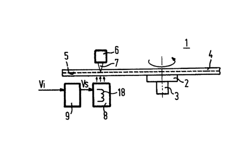
Figure 1 shows an embodiment of a magneto-optical
recording apparatus 1 in accordance with the invention.
record carrier 4 is rotated by a drive means com~rising
a turntable 2 and a motor 3. The record carrier 4 is
provided with a recording layer 5 of a magneto-optical
20 material of a customary type. By means of an optical head
6 a radiation beam 7, for example a laser beam, is aimed
at the recording layer 5. The magneto-optical material is
then heated to a temperature near the Curie point. By means
of a magnetic-field modulator 8 the heated portion of the
25 magneto-optical material is exposed to a magnetic field
of adequate strength to magnetize the heated portion in
a direction which depends on the direction of the magnetic
field. The magnetization persists after cooling. The mag-
netic modulator 8 modulates the magnetic field in conformity
30 with a control signal Vs which is derived from an information
signal Vi by an encoding circuit 9, for example an EFM
encoder. Thus, a pattern of magnetic domains representative
of the information signal is formed in the recording layer ~.
Figure 2 shows an example of a magnetic-field
35 modulator. A series arrangement of an electronic switch 11
and a diode lZ is arranged between a terminal lO at a
positive potential Vp and a node 13. A series arrangement
of an electronic switch 15 and a diode 16 is connected
6 ~ 9~8~
between the node 13 and a terminal 14 at a potential Vn
opposite to Vp. The node 13 is connected to one (17) of
the terminals of a field coil 18 for generating the magnetic
field. The other terminals 19 of the field coil 18 is
5 connected to a terminal 20 at earth potential. A capacitor
21 is arranged in parallel with the magnet coil 18. The
magnet coil 18 and the capacitor 21 together constitute a
parallel resonant circuit. The capacitance of the capacitor
21 is selected in such a way that the resonant period of
10 the resonant circuit is smaller than the maximum permissible
switching time required for the reversal of the magnetic
field. In an apparatus for recording standard E~M signals
a capacitance of 1 nF is suitable in conjunction with an
inductance of 5~1H
A control circuit 22 derives the control signal
for the electronic switches 11 and 15 from the control
signal Vs. The relationship between the states of the switches
11 and 15 and the logic values of the control signal Vs
is given in Table 1.
20 Table 1.
. jV9 switch 1 1 switch 15
0 open closed
25 1 closed open
,
The operation of the magnetic-field modulator 8
will now be explained with reference to ~igure 3.
At the instant tO the magnetic-field modulator
30 is in a stable state in which the logic value of control
signals Vs is "1", which means that the switch 11 is closed
and the switch 15 is open. The voltage Vm across the field
coil 18 is then equal to the potential difference (Vp)
between the terminal 10 and the terminal 20. The current
35 Im through the coil depends on the resistance of the field
coil 18. In the case of a resistance having a customary
value of 1 n and a customary desired current strength of
1 A the required potential difference can be as low as
. ,
7 ~ 3 1 ~
a few volts. In response to the ~ "O" transition of the
control signal Vs at the instant t1 the switch 11 is opened,
so that the resonant circuit comprising the field coil 18
and the capacitor 21 is uncoupled from the terminal 10.
5 In the resonant circuit this gives rise to a transient
effect in the form of a sinusoidal variation of the current
Im and the voltage Vm. Although the switch 15 is now closed
the coupling of the terminal 17 is inhibited by the diode
16 as a result of the high negative voltage ~5O-100 V)
lO induced in the field coil 18.
At the instant t2 the diode 16 is turned on, so
that the potential on the terminal 17 becomes equal to the
negative potential Vm. This instant t2 is situated substan-
tially half a resonant period after the instant t1 at which
5 the switch 11 is opened. At this instant the current has
decreased to a value Im, whose absolute value is equal to
the absolute value of the current at the instant t1 but
whose sign is opposite to the sign of the current at the
instant t1. As from the instant t2 the terminal 17 is
20 coupled to the terminal carrying the negative potential
Vn, the current value remains equal to In until at the
instant t3 the logic value of Vs again changes from ~'O"
to "1", so that the switch 11 is closed and the switch 15 is
opened again, the direction of the current Im being conse-
25 ~uentlY reversed.
In the embodiment shown in ~igure 2 the parallelresonant circuit comprises a parallel arrangement of the
field coil 18 and the capacitor 21. In practice, it is
found that in many cases it is not necessary to arrange
30 a capacitor across the magnet coil 18 because the parasitic
capacitance of the field coil, the switches and wiring
is adequate for a correct operation of the magnetic-field
modulator 8.
Further it is to be noted that the diodes 12
and 16 are not needed if the switches are controlled in
such a way that after one of the switches has been opened
the other switch is not closed until expiry of half a
resonant period. However, because of its simplicity and
8 t 3 `1 ~
i~munity to resonant-frequency variations the embodiment
comprising the diodes is to be preferred.
Figure 4 shows an embodiment of the magnetic-
field modulator 8 which can be powered by means of a single
5 direct voltage supply. Elements corresponding to those in
the embodiment shown in Figure 2 bear the same reference
numerals. The switch 11 comprises a transistor of the
p-FET type, which is available for example under the type
number BST 100. The switch 15 comprises a transistor of
10 the n-FET type, which is availbale for example under the
type number ~ST 70A. FET transistors are very suitable for
use as switches in the present magnetic-field modulator,
because these transistors are capable of withstanding the
high reverse voltages arising during change-over of the
15 switches. This is in contra distinction to bipolar transis-
tors, which can handle only substantially lower reverse
voltages and which in practice are therefore suitable only
for recording signals of comparatively low frequency.
Moreover, bipolar switching transistors which can handle
20 the required large currents and high reverse voltages have
substantially larger switching times than FET-transistors.
The control circuit 22 comprises two buffer amplifiers 30
and 31, which suitably form part of the same integrated
circuit, for example a circuit of the type 74HC125. This
~5 has the advantage that the delay times of the amplifier
circuits 30 and 31 are substantially equal to each other,
so that the instants of opening and closure of the switches
are well adapted to each other,
The embodiment shown in Figure 4 differs from
30 that shown in Figure 2 in that a capacitor 32 is arranged
between the node 13 and the terminal17 of t~ coil 18. The capacitor
32 ~ e~her wi~ the resonant circuit constitutes a high-pass
filter to eliminate the d.c. component. This has the advan-
tage that a single power supply can be used.
The embodiment shown in Figure 4 is very suitable
for recording d.c.-free encoded signals, such as for example
EFM modulated signals. In such d.c.-free encoded signals
9 ~ 31~9~
the average time during which the signal has the logic
value "1" is equal to the time that the logic value is "O".
~or the embodiment of ~igure 4 this means that the current
in, the coil is the same for both current directions, which
5 is desirable for magneto-optical recording because the
strength of the magnetic field should be the same for both
directions of magnetization.
~ igure 5 shows an embodiment of the magnetic-
field modulator which can also be powered by means of a
tO single power supply and which is also adapted to record
signals which are encoded in a non-d.c.-free manner.
In ~igure 5 elements corresponding to the elements
in Figure 2 and Figure 4 bear the same reference numerals.
In the present embodiment the node t3 and the terminal
15 19 constitute two diagonally opposite nodes of a bridge
comprising a first branch which comprises the switches
11 and 15 and the diodes 12 and 16 and a second branch
which is identical to the first branch and which comprises
the switches 1la, 15a and the diodes 12a, 16a. The switches
20 11 and 15 are controlled in the manner described above
by a control circuit 22, which derives the control signals
for the switches 11 and 15 from the control signal Vs.
The switches 11a and 15a are controlled in a similar way
by a control circuit 22a which is identical to the control
25 circuit 22. The control signals for the switches 11a and
15a are derived from the signal Vs which is derived from
the signal Vs by means of an inverter circuit 4O. In this
embodiment of the magnetic-field modulator rwo diagonally
opposite switches are closed while the other two switches
30 are open depending on the logic value of the control signal
Vs, so that the polarity of the voltage across the field
coil depends on the logic value of the control signal Vs.
Apart from the afore-mentioned advantage the
embodiment of ~igure 5 has the advantage that the high
35 induction voltage produced during uncoupling is divided
between two switches, so that very high induction voltages
can be handled.
lo i3~99~
~ ig. 6 shows another example of the magnetic-
field modulator 8. Between the terminal 10 and the terminal
14 a series arrangement is situated, which comprises, in
this order, a diode 60, an n-channel FET 61, a diode 62,
5 and an n-channel FET 63. Together with the capacitor 32
the parallel resonant circuit comprising the field coil 18
and the capacitor 21 again constitutes the high-pass filter,
which is arranged between a junction point 64 (between the
diode 60 and the transistor 61) and a junction point 65
10 ¦between the diode 62 and the transistor 63).
A non-inverting amplifier 69 and an inverting
amplifier 70 derive the drive signals A and A for the
transistors 61 and 63 respectively from the signal Vs.
These drive signals drive the FETs 61 and 63 in such a way
15 that alternately only one of these transistors 61 and 63
is turned on. When the transistor 63 conducts and the tran-
sistor 61 is cut off the field coil 18 is energized via the
current path comprising the diode 60, the field coil 18,
the capacitor 32 and the transistor 63. If subsequently
20 the transistor 63 is turned off and the transistor 61 is
turned on a trasient effect is produced in the resonant
circuit comprising the field coil 18 and the capacitor 21,
so that for a time interval corresponding to half the
resonant period of the resonant circuit an induction voltage
25 is produced, which keeps the diode 62 in the cut-off state.
At the end of said transient interval the current in the
field coil 18 is reversed and the diode is turned on again,
causing the capacitor 32 to discharge via the circuit com-
prising the diode 62, the transistor 61 and the field coil.
30 The capacitance of the capacitor 32 is selected in such a
way that it may be regarded as a short-circuit for the
frequencies with which the transistors 61 and 63 are switched.
If the drive signals A and A are d.c.-free as in the case
that ~FM-signals are recorded, this means that the voltage
35 across the capacitor 32 is always substantially equal to
half the voltage difference between the terminals 10 and 14,
so that the current through the field coil continually
11 ~3~
varies between a negative value and a positive value,
said positive and negative currents being equal in absolute
value. This is essential for magneto-optical recording
because during recording the magnetic fields thus produced
5 should have the same strength for both possible directions.
The magnetic-field modulator shown in Fig. 6
comprises two n-channel FETs instead of one p-channel EET
and one n-channel FET, as in the magnetic-field modulator
shown in Fig. 4. As the heat dissipation in the currently
10 available p-channel FETs is substantially higher than in
n-channel FETs the heat dissipation in the circuit for
energizing the field coil in the embodiment shown in Fig. 6
will be substantially lower than in the embodiment shown
in Fig. 4.
For a reliable operation of the circuit shown
in Fig. 6, however, it is desirable to couple the junction
point 66 between the transistor 61 and and the diode 62
to a point 68 of constant potential via an impedance 67.
This is because it is necessary that, in order to turn on
20 the transistor 61, the gate-source voltage of the transistor
should have a well-defined value. In the absence of the
impedance 67 the gate-source voltage would not be well-
defined during the time interval in which the diode 62
is cut-off. Moreover, it is to be noted that the circuit
25 shown in Fig. 6 may also be equipped with p-channel FETs
if the polarity of the voltage between the terminals 10
and 14 is reversed and, in addition, the cathodes and
anodes of the diodes 60 and 62 are interchanged.
Further, it is to be noted that in principle
30 the capacitor 21 may be replaced by two capacitors, one of
these capacitors being connected between the junction point
64 and the terminal 14 and the other capacitor being
connected between the terminal 14 and the junction point
71 between the field coil 18 and the capacitor 32. It is
35 alternatively possible to arrange the capacitor 21 between
the junction points 64 and 65. This is because the capacitor
32 may again be regarded as a short-circuit for the pre-
vailing switching frequencies.
` 12 ~3~9~'~
~ ig. 7 shows a field-coil energizing circuit
comprising four n-channel EETs 72, 73, 74 and 75 and a
bridge circuit. The parallel arrangement of the field coil
18 and the capacitor 21 is connected between two diagonally
5 opposed bridge nodes. The two other nodes of the bridge
are connected to the terminals 10 and 14. A diode 78 is
arranged between the transistor 72 and the junction point
76 and a diode 79 between the transistor 74 and the junction
point 77 in order to inhibit the current supply from the
10 d.c. source connected to the terminals 10 and 14 during
the re~ersal of the current in the field coil 18.
The use of low-dissipation n-channel EETs again ensures
a minimal dissipation in the circuit.