Note: Descriptions are shown in the official language in which they were submitted.
13201~2
- 1 -
TITLE OF TH~ INVENTION
Method for Forming a Deposited Film
BACKGROUND OF THE INV~NTION
Field of the Invention
This invention relates to a method for formation
of a deposited film useful for obtaining a functional
film, particularly a semiconductive film which is
useful for electronic devices such as semiconductor
device,optical input sensor device for an optical image
inputting apparatus, photosensitive device for electro-
photography, etc.
Related Background Art
In the prior art, for formation of functional
films, particularly crystalline semiconductor films,
suitable film forming methods have been individually
employed from the standpoint of desired physical
characteristics, uses, etc.
For example, for formation of silicon deposited
films such as of amorphous or polycrystalline, i.e.
non-single crystalline, silicon which are optionally
compensated for lone pair electrons with a compensating
agent such as hydrogen atoms ( H ) or halogen atoms (X),
etc., (hereinafter abbreviated as "NON-Si (H,X)",
particularly "A-Si (H,X) " when indicating amorphous
silicon and "poly-Si (H,X) " when indicating poly-
crystalline silicon) (the so-called microcrystalline
1~20102
-- 2
I silicon is included within the category of A-Si (H,X~
as a matter of course), there have been employed the
vacuum vapor deposition method, the plasma C~D method,
the thermal CVD method, the reactive sputtering method,
the ion plating method, -the optical CVD method, etc.
Generally, the plasma CVD method has been widely used
and industrialized.
However, the reaction process in formation of a
silicon deposited film according to the plasma CVD
method which has been generalized in the prior art ,is
considerably complicated as compared with the
conventional CVD method, and its reaction mechanism
involves not a few unclarified points. ~lso, there exist
a large number of parameters for formation of a
deposited film such as substrate temperature, flow
rate and flow rate ratio of gases to be introduced,
pressure during formation, high frequency power,
electrode structure, structure of a reaction vessel,
speed of evacuation, plasma generating system, etc.
20 By use of a combination of such a large number of .
parameters, plasma may sometimes become unstable state,
whereby marked deleterious influences were exerted
frequently on a deposited film formed. Besides,
parameters characteristic of film forming devices must
be selected for each device and therefore under the
present situation it has been difficult to generalize
the production condition.
,~
132~102
1 Also, in the case of the plasma CVD method,
since plasma is direc-tly generated by high frequency
or microwave, etc., in a film forming space in which a
substrate on which film is to be formed is placed,
electrons or a number of ion species generated thereby
may give damages to the film in the film forming
process to causa lowering in film quality or non-
uniformization of film quality. Moreover, the
condition suitable for crystallization of a deposited
film is restricted and therefore it has been deemed to
be difficult to produce a polycrystalline deposited film
with stable characteristics.
On the other hand, for formation of an epitaxial
deposited film such as of silicon, germanium, group
i5 II-VI or Group III-V semiconductors, etc., there have
been used the gas~phase epitaxy and the liquid phase
epitaxy as defined in a broad sense (generally speaking,
the strict definition of epitaxy is to grow another
single crystal on a single cxystal, both having the
same single crystal axes, but here epitaxy is interpreted
in a broader sense and it is not limited to the growth
onto a single crystal substrate).
The liquid phase epitaxy is a method for
precipitating a semiconductor crystal on a substrate by
dissolving a starting material for semiconductor at
high temperature to a super-saturated state in a solvent
metal which is molten to a liquid and cooling the
~ 4 ~ 132~1~2
I solution. According to this method, since crystals are
grown under a state most approximate to thermal
equilibrium among various epitaxy techniques, crystals
with high perfectness can be obtained, but on the other
hand, bulk productivity is poor and surface state is
bad. For such reasons, in an optical device which
requires an epitaxial layer which is thin and also
uniform in thickness, problems are accompanied such as
yield in device production, or influences exerted on
device characteristics, etc., and therefore this method
is not frequently used.
On the other hand, the gas phase epitaxy has
been attemp~ed by physical methods such as the vacuum
vapor deposition method, the sputtering method, etc.,
or chemical methods such as hydrogen reduction of a
metal chloride or ~therwise thermal pyrolysis of a
metal organic compound or a metal hydride. Among them,
the molecular beam epitaxy which is a kind of the
vacuum vapor deposition method is a dry process under
ultra-high vacuum, and therefore high purification and
low temperature growth of crystals are possible,
whereby there is the advantage that composition and
concentration can be well controlled to give a relatively
flat deposited film. However, in addition to an
enormous cost required for a film forming device, the
surface defect density is great, and no effective
method for controlling directionality of molecular beam
,...
- 5 - ~320102
1 has been developed, and also enlargement of area is
difficult and bulk productivity is not so high. Due
to such many problems, it has not been industrialized
yet.
The hydrogen reduction method of a metal chloride
or the ther~al pyrolysis method of a metal organic
compound or a metal hydride are generally called the
halide CVD method, the hydride CVD method, MO-CVD
method. For these methods, by the reason that a film
forming device can be made with relative ease and also
as the starting materials, i.e. metal chloride, metal
hydrides and organic metals, those with high purities
are now readily available, they have been studied widely
at the present time and application for various devices
has been investigated.
However, i-n these methods, it is required to heat
a substrate to a high temperature at which reduction
reaction or thermal pyrolysis reaction can occur and
therefore the scope of substrate material to be
selected is limited, and also contamination with
impurities such as carbon or halogen, etc., is liable
to cause if decomplsition of starting material is
insuf~icient, thus having the drawback that control-
lability of doping is poor. Also while, depending on
the application use of a deposited film, it is desired
to effect bulk production with reproducibility with
full satisfaction in terms of enlargement of area,
,...
~ 5 - 13~02
1 uniformization of film thickness as well ~s uniformness
of film ~uality and yet at a high speed film formation,
under the present situation no technique which enables
bulk production with maintaining practical characteris~ics
sa-tisfying the above demands has been established yet.
SUMMARY OF THE INVENTION
. .
A principal object of t:he present invention is
to provide a method for forming a deposited film which
is easy in control of film quality simultaneously
with saving energy and can give a crystalline deposited
film having desired characteristics uniformly over a
large area and excellent in semiconductive characteristics.
Another object of the present invention is to
provide a method for forming a deposited film which is
excellent in productivity and bulk productivity and can
form simply and efficiently a crystalline deposited film
having high quality and excellent physical character-
istics such as electrical, optical or semiconductive
characteristics, etc.
The present invention has been accomplished as
the xesult of intensive studies which have been made by
: the present inventors in order to achieve the objects
of the present invention as mentioned above by solving
the various problems as described above, and it is a
method for forming a deposited film, comprising the step
(A) of introducing a starting material (A) which is
,_
- 7 - ~3201~2
I either one of a gaseous starting material for formation
of a deposlted film and a gaseous halogenic oxidizing
agent having the property of oxidative action on said
starting material into a film forming space in which a
substrate having a material which becomes crystal
neclei for formation of a deposited film to be formed
thereon or a material capable of selectively forming
crystal nuclei scatteringly on its surface is previousl~
arranged to have said starting material adsorbed onto
the surface of said substrate to form an adsorbed layer
(I) and the step (B) of introducing the other starting
material (B) into said film forming space, thereby
causing the surface reaction on said adsorption layer
(I) to form a crystalline deposited film (I).
The method for forming a deposited film of the
present invention-having the above constitution has one
specific feature in forming a deposited film by use of
a gaseous halogenic oxidizing agent without utilizing
plasma reaction while the plasma CVD method of the prior
art forms plasma discharging by permitting discharging
energy, etc., to act on starting gases for formation
of a deposited film, and therefore, it has the
advantage that no bad influence by etching or abnormal
discharging, etc., during film formation will not be
raised.
Also, the method for forming a deposited film
of the present invention has another specific feature
,,
- 8 - 1 3 2 ~ 1 ~ 2
I in forming a very thin deposited film on a substrate
by making either one of a gaseous starting material and
a gaseous halogenic oxidizing agent showing an o~idation
action on said starting material adsorbed onto the
substrate surface to form an adsorbed layer before
introduction of the other, and by doing so there is
the advantage that a deposited film with uniform film
thickness and uniform film quality can be obtained.
Also, the method for forming a deposited film
of the present invention utilizes the redox reaction of
a gaseous starting material which becomes the
constituent elements of the deposited film with a
gaseous halogenic ocidizing agent and requires no high
temperature for deposition, and therefore there is no
disturbance of structure by heat, and no heating
installation duri-ng production and no expense
accompanied with running thereof are required, whereby
a device can be made lower in cost. And, it becomes
possible to select the substrate material from a wide
scope of materials without depending on heat
resistance.
Also, the method for forming a deposited film
of the present invention forms a deposited film
according to the reaction between a gaseous starting
2~ material and a gaseous halogenic oxidizing agent which
progresses as concerned with the adsorbed molecules,
and therefore enlargement of area is facilitated not
- 9 1320102
1 depending on the shape and the size of the substra~e,
and at the same time starting materials employed may
be very small in amounts, whereby the film forming
space can be made smaller to improve dramatically the
Yield.
Also, the method for forming a deposited film
of the present invention can determine the sizes of
crystal grains by arranginy nuclei for crystal growth
as desired on a substrate, ~hereby a crystalline
deposited film having the characteristics suited for
the purpose can be deposited at any desired region.
Also, according to the method for forming a
deposited film of the present invention having the
constitution as described above, energy during forma-
tion of deposited film can be saved and at the sametime control of film quality can be easily practiced,
whereby it becomes possible to form a good crystalline
deposited film having uniform film quality and
characteristics over a large area. Further, it is
possible to obtain efficiently a crystalline film
which is excellent in productivity and bulk productivity,
of high quality and also excellent in various
charactexistics such as electrical, optical, semi-
conductive characteristics, etc.
BRIEF DESCRIPTION OF THE DRAWINGS
Fig. l is a schematic illustration of the film
13201~2
-- 10 --
I forming de~ice used in Examples of the present in1~enti~n
Fig. 2 shows an embodiment of the film forming
steps according to the present invention.
Fig. 3 shows an another embodiment of the film
forming steps according to the present invention.
Fig. 4 shows a further embodiment of the film
forming steps according to the present invention.
DRSCRIPTION OF THE PREFERRE~ EMBODIMENT
In the method for forming a deposited film of
the present invention, the gaseous starting material to
be used for formation of a deposited film (hereinafter
called "gaseous starting material (I)") is a material
to be subjected to oxidation action through contact
with the gaseous halogenic oxidizing agent (hereinafter
called "halogenic oxidizing agent (II)"), and may be
selected suitably as desired depending on the kind,
characteristic, use, etc., of a deposited film to be
desired. In the method of the present invention, the
above gaseous starting material (I) and the halogenic
oxidizing agent (II) have only to be gaseous when
introduced, and may be gaseous, liquid or solid under
an ordinary state. In the case when the gaseous
starting material (I) or the halogenic oxidizing agent
(II) is liquid or solid under an ordinary state, a
carrier gas such as Ar, He, N2, H2, etc., is used to
effect bubbling, optionally with heating, and thereby
1~2~02
1 introduce the gaseous starting material (I) or the
halogenic oxidizing agent (II) in a gaseous state into
a film forming space to form an adsorbed la~er on a
substrate, and then the other material is introduced in
a gaseous state.
During this operation, the introducing pressure
of the above gaseous starting material (I) or the
halogenic oxidizing agent (II) may be set by
controlling the flow rate of the carrier gas or the
vapor pressure of the gaseous starting material (I? or
the halogenic oxidizing agent (II). When the gaseous
starting material (I) or the halogenic oxidizing agent
(II) is a gas under an ordinary state, it can be also
introduced as diluted with a carrier gas such as Ar,
He, N2, H2, etc., if necessary.
As the gaseous starting material (I) to be used
1n the method of the present invention, for obtaining
a deposited film of e.g. silicon belonging to the
group IV of the periodic table, there may be employed
straight and branched chain silane compounds, cyclic
silane compounds, etc., as effective ones.
Specifically as the gaseous starting material
(I), examples of the straight chain silane compounds
may include SinH2n+2 (n = 1, 2, 3, 4, 5, 6, 7 or 8),
Z5 examples of the branched chain silane compounds
SiH3SiH(SiH3)SiH2SiH3, and examples of cyclic silane
compounds SinH2n (n = 3, 4, 5 or 6), etc.
- 12 - ~3~ 2
1 of course, these silicon compounds may be used
in the method of the present invention is made yaseous
when introduced into a film forming space and at the
same time has the property of exerting o~idation action
effectively on the gaseous starting material (I) for
formation of a deposited film only through contact
therewith, and halogenic gases such as F2, C12, Br2, I2,
ClF, etc., may be employed as effective ones.
Either one of these gaseous starting material
(I) and halogenic oxidizing agent (II) is first
introduced in a gaseous state at a desired flow rate and
feeding pressure into a film forming space in which a
substrate for formation of a deposited film is arranged
to form an adsorbed layer on said substrate, and then
the other is introduced after a desired time with a
desired flow rate~and feeding pressure, whereby the both
are collided against each other on the surface of the
above adsorbed layer to cause a surface chemical
reaction, whereby the above halogenic oxidizing agent
(II) exerts oxidation reaction on the above gaseous
starting material (I) to form a deposited film on the
substrate having a material which becomes the crystal
nuclei for a deposited film to be formed or a material
capable of forming selectively crystal nuclei
- 25 scatteringly on the surface. Such deposited film
forming process of the present i.nvention can proceed
with higher efficiency and energy saving degree, whereby
-
- 13 1320~02
I a deposited film having desired good physical c~arac~er-
istics over the ~hole film surface can be formed a~ a
lower substrate temperature than in the prior art.
In the method of the present invention, so that
the deposited film forming process may proceed smoothl~
and a film having desired physical characteristics of
high quality may be formed, as film forming factors,
kinds and combination of the starting material for
formation of a deposited film (I) and the halogenic
oxidizing agent (II), pressure during reaction, flow
rate, inner pressure of the film forming space, kind
of the substrate, pressure during adsorption, flow
pattern of the gases, adsorption temperature and film
forming temperature (substrate temperature and
atmosphere temperature) may be selected suitably as
desired. These f-ilm forming factors are related
organically, and they are not determined individually
but determined respectively under mutual relationships.
In the method of the present invention, the process of
adsorption and reaction of the gaseous starting material
(I) for formation of a deposited film and the gaseous
halogenic oxidizing agent (II) to be introduced into
the film forming space may be determined suitably as
desired in the relationship with film forming factors
concerned among the film forming factors as mentioned
above.
The conditions of the step of forming an adsorbed
.
- 14 - 1320102
I layer on the substrate in the method for forrniny a
deposited film of the present invention are suitably
set.
In adsorption of gas molecules onto a solid
surface, there exists intramolecular force, and ~he
chemical adsorption with valence energy is greater in
its intramolecular force than the physical adsorption
with dispersion energy (corresponding to Van der Waals
force).
Also, while physical adsorption is liable to
become a multi-layer adsorption, a chemical adsorption
is a monomolecular layer adsorption, and therefore
preferably for controlling deposition of a homogeneous
thin film, the adsorption should finally be in the
form of chemical adsorption.
However, in the process of the present
invention, the steps of adsorbed layer formation
through deposited film formation, physical adsorption
and chemical adsorption of gas molecules may be
considered to be related with each other complicatedly,
and the form of adsorption is not necessarily limited.
On the other hand, the factors which determine the
adsorption state may include the kind of adsorbed
molecules, the kind of solid surface an~ the surface
state, and further temperature and pressure as
controlling factors, and it is at least necessary to
determine these controlling factors so that the
,~
-` 1320102
- 15 -
1 reaction may be carried out to gi~/e a desired depo~ited
film.
That is to say, if the pressure in the vacuum
chamber in the cause from adsorption and the reaction
is too low, desorption from the state of physical
adsorption is liable to occur, while if the temperature
is too high, dissociating adsorption from the state of
chemical adsorption is liable to occur, and therefore
the reaction process suitable for a desired deposited
film must be selected.
In one cycle for formation of a deposited film
of the present invention (the step (A) of adsorbed
layer formation and the step (B) of deposited film
formation through reaction between the adsorbed layer
and the starting material), there are included the
following steps prior to uniform formation of a
deposited film on the substrate surface: The step of
introducing the starting material A into the film
forming space and permitting it in a suitable amount
adsorbed on the substrate to form an adsorbed layer
(the first step; step (A)) and the s-tep of permitting
the adeorbed layer of the starting material A to
remain while discharging superfluous starting material
A (the second step). In these steps, the pressures may
be set suitably for the above reasons, and the pressure
in the first step may be preferably higher for
sufficient progress of adsorption, preferably 1 x 10 7
1 3 ~ 2
- 16 -
I to 10 Torr, more preferably 1 x 10 to 1 Torr.
The pressure in the second step may be
preferably lower for discharging superfluous star~ing
material A, preferably 1 x 10 1 to 1 Torr, more
5 preferably 1 x 10 to 1 x 10 Torr.
Further, one cycle for formation of a deposited
film of the present invention comprises subsequent to
these steps the step of introducing the starting
material B to cause the surface reaction with the
adsorbed layer on the substrate to form a deposited
film (the third step; step (B)), and the next step of
discharging by-products formed other than the deposited
film at this time (the fourth step), and the pressure
during the reaction in the third step may be preferably
higher in order to enhance the probability of the
contact between the starting materials A and B, but the
final value is determined suitably as desired in view
of the reactivity.
The pressure in the third step may be
20 preferably 1 x 10 8 to 10 Torr, more preferably 1 x 10 6
to l Torr.
The pressure in the fourth step may be
preferably 1 x 10 to 1 Torr.
In the present invention, the aforementioned
steps (A) and (B) are conducted at least once, and
depending on the case, steps (A) and (B) may be repeated
in this order as required. In that case, the time
1320102
I required for each step (A) or (~) may be constant ~r
varied over the whole cycles.
In the method of the present invention, for
forming selectively a desired crystalline deposited film,
it is necessary to arrange previously a material ~,7hich
becomes crystal nuclei for a deposited film to be
formed or a material capable of forming selectively
crystal nuclei in the form corresponding to the purpose
regularly or irregularly scatteringly on the substrate
surface.
In the former case, by arrangement of single
crystalline grains on the substrate, a crystal can be
selectively grown with the single crystalline grains
becoming crystal nuclei.
lS Also, by selecting suitably the film forming
conditions and the-kind of crystalline material which
become crystal nuclei, crystalline deposited films of
different kinds can be selectively formed.
In the case of the latter, by utilizing the
difference in nuclei formation density of the
depositing material according to the kinds of the
materials of the deposited surface, by arranging a
different kind of material from the material of the
substrate surface scatteringly with a desired pattern
on the substrate, a desired crystalline deposited film
can be formed selectively.
As the substrate to be used in the former case,
--` 1 32~102
- 18 -
I a substrate with small gro~Jth of silicon crystals having
silicon single crystal grains arranged thereon may 'oe
employed, Further, in place of the silicon crystal as
described above, crystals different in kind from silicon
may be also used as the nuclei, but the materials of
these crystals are required to satisfy the follo~liny
conditions.
1. The lattice constant of the crystalline
material on the substrate surface should be identical
with or very approximate to the lattice constant of the
deposited film.
2. The coefficients of thermal expansion of the
crystalline material on the substrate surface and the
deposited film should be identical with or very
approxlmate to each other.
Hence, as the material which should constitute
the surface of a suitable substrate for obtaining a
deposited film of e.g. crystalline Si, there may be
included GaF2, ZnS, Yb, Mn3Ga, NaCoF3, Ni3Sn, Fe3C,
NiTex (x < 0.7), CoMnO3, NiMnO3, MaZn3, CuCl, AlP,
Si, etc.
Further, even when the above two conditions
are not fully satisfied, by selecting the deposition
conditions more adequately, a crystalline deposited
film can be also obtained, and the method for forming
a deposited ~ilm of the present invention is not
limited to the materials only as described above.
1320102
- 19 -
I As the substrate to be used in the latter case,
for example, those having Si3N4 arranged scatteringly
on SiO2 film or those having SiO2 covering over Si3~4
film to have partially the subbing Si3N4 exposed may
be employed.
These substrates utilize the property of silicon
crystal nuclei which are formed with ease on Si3N4 and
with difficulty on SiO2, and in the method for forming
a deposited film of the present invention, both amorphous
and crystalline materials can be used, provided they
have difference in difficultly and easiness in formation
of nuclei.
The substrate temperature (Ts) during film
formation may be set suitably depending on the kind of
the deposited film to be formed and the kind of the
substrate used.
The method of the present invention is described
in more detail by use of Examples, but the present
invention is not limited by these Examples.
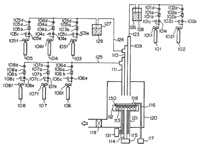
Fig. 1 shows one example of a preferable device
for embodying the method for formation of a deposited
film of the present invention.
The device for forming a deposited film shown
in Fig. 1 is divided broadly into three parts of the
main device, the discharging system and the gas feeding
system.
The main device is provided with a film forming
space.
132~02
- 20 -
I 101 to 108 are respectively bomhs filled ~"ith
the gases to be used during film formation, lOla-108a
are respectively gas feeding pipes, lOlb-108b are
respectively mass flow controllers for controlling the
flow rates of the gases from the respective bombs,
lOlc-108c are respectively gas pressure gauges, lOld-
108d and lOle-108e are respectively valves, and lOlf-
108f are respectively pressure gauges indicating the
pressures in the corresponding gas bombs.
120 is a vacuum chamber, having a structure
such that a pipeline for introduction of gas is provided
at the upper portion and a reaction space is formed
downstream of the pipeline, and also having a structure
such that a film forming space provided with a
substrate holder 112 may be formed so that a substrate
118 may be placed-as opposed to the gas introducing inlet
of said pipeline. The pipeline for introduction of gas
has a three-arrangement structure, having from the
innerside a first gas introducing pipe 109 for introduc-
ing gases for the gas bombs 101, 102, a second gasintroducing pipe 110 for introducing the gases from the
gas bombs 103-105, and a third gas introducing pipe 111
for introducing the gases from the gas bombs 106-108.
Feeding of the gases from the bombs to the
respective introducing pipes is done through the gas
feeding pipelines 123-125, respectively.
The respective gas introducing pipes, the
-- 1320~02
- 21 -
I respective gas feeding pipelines and the vacuum chamber
120 are evacuated to vacuum by a vacuum evacuating
device not shown through the main vacuum valve 119.
The substrate 118 can be set freely at any
desired position relative to the respective gas introduc-
ing pipes by moving the substrate holder 112 verticall~
and in the directions of X and Y.
In the case of the method of the present
invention, the distance between the substrate and the
gas introducing inlet of the gas introducing pipe may
be determined appropriately in view of the kinds of the
deposited film to be formed, its desired characteristic~,
gas flow rates, the inner pressure of the vacuum chamber,
etc., but it should preferably several mm to 20 cm,
more preferably about 5 mm to 15 cm.
130 is a cooling pipe for making the gas
molecules of the starting material A easily adsorbable
onto the substrate 118, and it is connected to the flow
rate controller 131. Cooling can be also used during
film formation or after film formation other than in
the first and the second steps in which adsorption is
effected.
113 is a heater for heating the substrate,
which heats the substrate 118 to an appropriate
temperature during film formation, preheats the
substrate 118 before film formation, and further, after
film formation, heats the film for annealing.
: ' '
132~1~2
- 22 -
I To the heater for heating the substra~e 113 is
fed power from t~e power source 115 through the wire
114.
116 is a thermocouple for measuring the
temperature of the substrate (Ts) and is connected
electrically to the temperature display device 117.
126 and 127 are bubblers for liquid starting
materials, and used with filling of liquid starting
materials for formation of a deposited film 128 and
129. When the starting materials for formation of a
deposited ~ilm are gases under an ordinary state, it is
not necessary to use bubblers for liquid starting
materials.
Example 1
By means of the film forming device shown in
Fig. 1, a deposited film according to the method of the
present invention was prepared as described below.
SiH4 gas filled in the bomb 101 was fed at a
flow rate of 40 sccm through the gas introducing pipe
20 109, F2 gas filled in the bomb 106 at a flow rate of
60 sccm and the ~e gas filled in the bomb 107 at a flow
rate 120 sccm through the gas introducing pipe 111 into
the vacuum chamber 120. In this Example, the bubblers
126 and 127 for liquid starting materials were not used.
The substrate 118 was prepared according to the
steps shown in Fig. 2.
First, a polycrystalline silicon substrate 201
~ 320102
- 23 -
1 as shown in Fig. 2(A) was washed, and subsequently
silicon oxide thin film 202 was deposited on the whole
surface of the substrate 1 according to the sputtering
method (in this step other various thin film depositing
methods such as vacuum vapor deposition, plasma discharg-
ing, MBE, CVD, etc., may be employed3 (Figure 2(B)).
Subsequently, an electron beam resist layer 203
was formed on the thin film 202 (Figure 2(C)~, and the
electron beam resist layer 203 exposed to light by use
of a photomask with a desired pattern and the electron
beam resist layer 203 was partially removed by
development (Figure 2~D)).
With the use of the remaining electron beam
resist 203A as the mask, the silicon oxide thin film 202
was subjected to etching to form a thin film 202A with
a desired pattern-(Figure 2(E)).
According to the steps as described above, a
substrate 118 with the crystal faces where a poly-
crystalline silicon exists were exposed at constant
zO intervals from the silicon oxide film was obtained.
The domains of the silicon crystal exposed on the
substrate surface were 500 A in width, with intervals
of 300 ym therebetween.
Next, the vacuum chamber 120 was evacuated under
sufficient baking by means of an evacuating device not
shown to 5 x 10 9 Torr. SiH4 gas filled in the bomb 101
was permitted to flow at a flow rate of 4 sccm through
132~102
- 24 -
I the gas introducing pipe lO9 into the vacuum chamber
120 for 0 . 3 sec under the state maintained at an
evacuating speed o~ 0.1 rn Torr/cm by controlling the
evacuating valve 119. Subsequently, the valve 101d was
closed to stop feeding of SiH4 gas, and the state
controlled to a vacuum degree of 0.01 Torr by opening
the evacuating valve 119 was maintained for 2 sec.
F2 gas (diluted to 10 % with He) filled in the
bomb 107 was introduced at 4 sccm through the gas
introducing pipe 111 into the vacuum chamber 120. The
evacuation rate at this time was controlled to 0.8 m
Torr/sec by controlling the evacuating valve 119, and
after this state was maintained for 5 sec, the valve
107a was closed to stop feeding of F2 gas, and the
state controlled to a vacuum degree of 0.004 Torr by
opening the evacuation valve 119 was maintained for
3 sec.
By repeating the operation as described above
for 4200 times, a crystalline silicon deposited film 204
with a thickness of about 4600 A was obtained.
Fig. 2(F) shows schematically the cross-
section of the crystalline silicon deposited film 204
obtained on the substrate 118. 205 denotes grain
boundaries in Fig. 2(F).
Further, by the use of the respective samples
obtained, crystallinity of the deposited films was
evaluated by the X-ray diffraction method and the
,..
- ` 13~102
- 25 -
1 electron beam diffraction method, whereby they ,wer~
confirmed to be polycrystalline films. Further, the
grain size of the polycrystalline silicon was found to
be about 250 +20 ym. Variance in crystal grain sizes
was uniform over the whole surface of the substrate,
When the surface state of the samples was
observed by a scanning type electron microscope, the
smoothness was good without wavy pattern, etc., and
the film thickness irregularity t was +4 ~ or less.
Also, the mobility and conductivity of the crystalline
Si deposited film of the obtained samples was measured
by the Van der Pauw method to be 250 (cm/V sec),
5 x 10 5 (S cm 1), respectively.
Example 2
The substrate 118 was prepared according to
the steps shown i~ Fig. 3.
First, a glass base plate 301 of a material
having substantially uniform composition as shown in
Fig. 3(A) was washed and then an amorphous SiN (A-SiN)
thin film 302 was formed with a thickness of about 2 pm
on the whole surface of the base plate 301 (Figure 3(B))
by means of thermal CVD.
Subsequently, surface annealing of the above
A-SiN thin film 302 was effected in N2 atmosphere by
means of a laser annealing device on the A-SiN thin
film 302 to form crystalline Si3N4 (C-Si3N4) 303
in the surface layer (up to 1 ~m deep of the A-SiN thin
132~02
~ 26 -
I film 302 to 1 ~um (Figure 3(C)).
As the laser used at this time, Ar-CW laser of
4880 A, a scanning speed of 2.5 cm/sec and an energy
of 10 W was irradiated. Subse~uently, the surface of
the C-Si3N4 layer 303 was scanned by means of the above
laser annealing device in 2 atmosphere to form
selectively the SiO2 layer 304 ~Figure 3(D~).
According to the steps as described above, a
substrate 118 having C-Si3N4 layer 303A exposed at
constant intervals with other portions being covered
with SiO2 layer 304 was formed. The domains of C-Si3~4
layer 303A exposed on the substrate surface were about
300 ~m in width with intervals of 200 ~um therebetween.
Further, by use of this substrate 118,
crystalline silicon was deposited by means of the device
shown in Fig. 1 si~ilarly as described in Example 1.
~ irst, the vacuum chamber 120 was evacuated
under sufficient baking by means of an evacuation
device not shown to 5 x 10 9 Torr. Siff4 gas filled in
the bomb 101 was permitted to flow for 0.3 sec at a
flow ~ate of 5 sccm into the vacuum chamber 120 through
the gas introducing pipe 109 under the state maintained
at an evacuation speed of 0.1 m Torr/sec by controlling
the evacuating valve 119. Subsequently, the valve lOld
was closed to stop feeding of the SiH4 gas, and the
evacuation valve 119 was opened and the state controlled
to a vacuum degree of 0.1 Torr was maintained for 2 sec.
., .
~ 132~1~2
- 27 -
1 F2 gas (diluted to 10 ~ with He) filled in the
bomb 107 was introduced at 6 sccm through the gas
introducing pipe 111 into the vacuum chamber 120. The
evacuation rate at this time was made 0.8 m Torr/sec
by controlling the evacuation valve 119, and after this
state was maintained for 5 sec, the valve 107a was
closed to stop feeding of the F2 gas, and the state
controlled to vacuum of 0.01 Torr was maintained for
4 sec by opening the evacuation valve 119.
By repeating this operation for 4500 times, a
crystalline silicon deposited film with a thickness of
about 2.3 ,um was obtained.
Fig. 3(F) shows schematically the cross-section
of the crystalline silicon deposited film 305 obtained
on the substrate 118. 306 denotes grain boundaries in
Fig. 3(F).
Further, by use of the respective samples
obtained, crystallinity of the deposited films was
evaluated by the X-ray diffraction method and the
electron beam diffraction method, whereby they were
confirmed to be polycrystalline silicon films. Further,
the g~ain size of the polycrystalline silicon determined
by the Scherrar method was found to be about 120+25 lum.
Variance in crystal grain sizes was uniform over the
whole sur~ace of the substrate.
When the surface state of the sample was
observed by a scanning type electron microscope, the
13201~2
- 28 -
I smoothness was good without wavy pattern, etc., ~nd the
film thickness irregularity was +4 ~ or less. Also,
the mobility and conductivity of the crystalline Si
deposited film of the obtained samples was measured by
the Van der Pauw method to be 120 (cm/V sec), g Y~ 10 6
(S cm 1), respectively.
Example 3
By means of the film forming device shown in
Fig. 1, a deposited film according to the method of the
present invention was prepared as described below.
SiH4 gas filled in the bomb 101 was fed at a
flow rate of 40 sccm through the gas introducing pipe
109, F2 gas filled in the bomb 106 at a flow rate of
60 sccm and the He gas filled in the bomb 107 at a
15 flow rate 120 sccm through the gas introducing pipe 111
into the vacuum chamber 120. In this Example, the
bubblers 126 and 127 for liquid starting materials
were not used.
The substrate 118 was prepared according to the
steps shown in Fig. 4.
First, a polycrystalline silicon substrate 401
as shown in Fig. 4(A) was washed, and subsequentlv
amorphous SiO2 thin film 402 was d~posited on the whole
surface of the substrate 401 according to the sputtering
method (in this step other various thin film depositing
methods such as vacuum vapor deposition, plasma
discharging, MBE, CVD, etc., may be employed) Figure 4(B)).
1320~02
- 29 -
1 Then, amorphous Si3N4 thin film 403 was deposi~ed on said
SiO2 thin film 402 C~igure 4(C)].
Subsequently, an electron beam resist layer 404 "as
formed on the thin filrn 403 LFigure 4(D)~, and the electron
beam resist layer 404 exposed to light by use of a photo-
mask with a desired pattern and the electron beam resist
layer 404 was partially removed by development ~Figure 4(E)l.
With thé use of the remaining electron beam resist
layer 404A as the mask, the Si3N4 thin film 403 was subjected
to etching to form Si3N4 thin film 403A with a desir,ed
pattern ~Figure 4IF)~.
According to the steps as described above, a
substrate 118 where the surface of the SiO2 layer 402 was
exposed at constant intervals from the Si3N4 thin film 402
was obtained. The above Si3N4 thin film portions were
arranged on the Si~ thin film 402 at a width of 200 ~m
and an interval of 200 pm.
Next, the vaccum chamber 120 was evacuated under
sufficient baking by means of an evacuating deviGe not shown
to 5 x 10 9 Torr. SiH4 gas filled in the bomb 101 was
permitted to flow at a flow rate of 4 sccm through the gas
introducing pipe 109 into the vaccum chamber 120 for 0.3
sec under the state maintain~d at an evacuating speed of
0.1 mTorr/cm by controlling the evacuating valve 119.
Subsequently, the valve lOld was closed to stop feeding
of SiH4 gas, and the state controlled to a vacuum degree
of 0.01 Torr by opening the evacuating valve 119 was
, . ..
1~2~102
- 30 -
I maintained for 2 sec.
F2 gas (diluted to 10~ with He) filled in the bomb
107 was introduced at 4 sccm throuyh the gas introducing
pipe 111 into the vaccum chamber 120. The evacuation rate
at this time was controlled to 0.8 mTorr/sec by controlling
the evacuating valve 119, and after this state was maintained
for 5 sec, the valve ~07a was closed to stop feeding of
F2 gas, and the state controlled to a vacuum degree of
0.004 Torr by opening the evacuation valve 119 was main-
tained for 3 sec.
By repeating the operation as described above for10000 times, a crystalline silicon deposited film 405 with
a thickness of about 3.0 jum was obtained.
Fig. 4(G) shows schematically the cross-section
of the crystalline silicon deposited film 405 obtained on
the substrate 118.
Next, by the use of the respective samples obtained,
crystallinity of the silicon deposited films was evaluated
by the X-ray diffraction method and the electron beam
diffraction method, whereby they were confirmQd to be
polycrystalline silicon films. Further, the grain size
of the polycrystalline silicon determined by the Scherrar
method was found to be about 40 ~ 0.5 ,um. Variance in
crystal grain sizes was uniform over the whole ~urface of
the substrate.
When the surface state of the samples was observed
by a scanning type electron microscope, the smoothness was
- 31 _ ~32~102
I good without wavy pattern, etc., and the film thickn~Ds
irregularity t was +4% or less. Also, the mobilit~ and
conductivity of the crystalline Si deposited film of the
obtained samples was measured by the Van der Pau~7rnethod
to be 300 (cm/V sec), 9 x 10 6 (S cm 1), respectively.
Example 4
The substrate 118 was prepared according to the
steps shown in Fig. 4.
First, a glass base plate 401 of a material having
substantially uniform composition as shown in Fig. ,4(A)
was washed and then an amorphous SiN:H thin film 402 was
formed using SiH4 gas and NH3 gas with a thickness of
about 2 ~m on the whole surface of the base plate 401
CFigure 3(B)~ by means of plasma CVD.
lS Subsequently, an amorphous SiO2 thin film 404 was
formed to 500 A thick on the above SiN:~ thin film 402 by
means of the sputtering method rFigure 4(C)~.
Then, an electron beam resist layer 404 was applied
onto the SiO2 thin film 403 LFigure 4(D)~, and the electron
beam resist layer 404 was exposed with the use of a photo-
mask having a desired pattern followed by partial removal
of the electron beam resist layer 404 by development
~Figure 4(E)~, The SiO2 layer 403 was then subjected to
etching to form an SiO2 layer 403A having a desired pattern
with utilizing the remaining electorn beam resist layer
404A as a mask.
According to the steps as described above, a
.v
- 32 - 1~20102
1 substrate 118 having domains 402A where the Si3eJ4 la~er
402 was exposed at constant intervals with other portions
being covered with SiOz layer 403A was formed, The domains
of Si3N4 layer 402A exposed on the substrate surface ~ere
about 300 ~um in width with intervals of 280 ~m therebetween.
Further, by use of this substrate 118, crystalline
silicon was deposited by means of the device shown in Fig.
1 similarly as described in Example 3.
First, the vacuum chamber 120 was evacuated under
sufficient baking by means of an evacuation device not
shown to 5 x 10 9 Torr. SiH4 gas filled in the bomb 101
was permitted to flow for 0.3 sec at a flow rate of 5 sccm
into the vacuum chamber 120 through the gas introducing
pipe 109 under the state maintained at an evacuation speed
of 0.1 mTorr/sec by controlling the evacuating valve 119.
. Subsequently, the valve lOld was closed to stop feeding
of the SiH4 gas, and the evacuation valve 113 was opened
and the state controlled to a vacuum degree of 0.1 Torr
was maintained for 2 sec.
F2 gas (diluted to 10~ with He) filled in the bomb
107 was introduced at 6 sccm through the gas introducing
pipe 111 into the vacuum chamber 120. The evacuation
rate at this time was made 0.8 mTorr/sec by controlling
the evacuation valve 119, and after this state was main-
tained for 5 sec, the valve 107a was closed to stop feeding
of the F2 gas, and the state controlled to vacuum of 0.01
Torr was maintained for 4 sec by opening the evacuation
~320102
- 33 -
I valve 119.
By repeating this operation for 7000 times, a
crystalline silicon deposited film with a thickness of about
2.8 ~m was obtained.
Fig. 4(G) shows schematically the cross-section
of the crystalline silicon deposited film 405 obtained on
the substrate 118.
Further, by use of the respective samples obtained,
crystallinity of the deposited films was evaluated by the
X-ray diffraction method and the electron beam diffraction
method, whereby they were confirmed to be polycrystalline
silicon films. Further, the grain size of the poly-
crystalline silicon was found to be about 90 + 7 ~m.
Variance in crystal grain sizes was uniform oYer the whole
surface of the substrate.
When the surface state of the sample was observed
by a scanning type electron microscope, the smoothness was
good without wavy pattern, etc., and the film thickness
irregularity was +4~ or less. Also, the mobility and
conductivity of the crystalline si deposited film of the
obtained samples was measured by the Van der Pauw method
to be 120 (cm/V sec), 4 x lO 6 (S cm 1), respectively.
The method for forming a deposited film of the
present invention can form a deposited film only by
contacting a gaseous starting material with a gaseous
halogenic oxidizing agent, and has the advantage of
requiring particularly no reaction exciting energy from
.~
1~201~2
- 34 -
I the outside. Accordingly, it becomes possible to lower
the substrate temperature. Also, since a material which
becomes the crystal nucleus for the deposited film or
capable of forming selectively the crystal nucleus can be
S arranged at a desired position on the substrate surface,
any desired crystalline deposited film can be formed.
Further, simultaneously with saving of energy, it is possible
to obtain a crystalline deposited film having uniform film
quality and characteristics over a large area with easy
control of the film quality. Further, a crystallinç film
excellent in productivity, bulk productivity and having
high quality with excellent electrical, optical semi-
conductive and other physical properties can be obtained
with ease.