Note: Descriptions are shown in the official language in which they were submitted.
1320259
BACKGROUND OF THE INV~NTION
Field of the Invention:
The present invention relates to broadband signal
switching equipment and more particularly to cross point matrices
constructed in field effect transistor technology.
Descri~tion of the Prior Art
If emitter-coupled logic (ECL) technology can be
characterized by properties such as high working speed,
moderately high degree of integration and moderately high
dissipatéd power, then field effect transistor (FET) technology,
given only moderate working speeds in comparison thereto,
however, is distinguished by an extremely high degree of
integration and by extremely low dissipated powers. These latter
properties lead to efforts to penetrate into speed regions
previously reserved for the bipolar technique with integrated
circuits in FET technology.
Known in this context, ~rom EP-A-0 264 046, is a
broadband signal switching equipment comprising a crosspoint
matrix that comprises matrix input lines respectively formed with
two ~ignal conductors which, first of all, are respectively
connected to two dif~erential (complementary) outputs o~ an input
digltal signal circuit and, secondly, can be connected via
crosspoints to matrix output lines that likewise are respectively
~ormed with two signal conductors. These matrix output lines
have their two signal conductors respectlvely connected to the
two signal inputs of an output amplifier circuit formed with a
di~erential ampli~ier. A crosspoint matrix constructed in FET
technology therefore has pairs o~ switching elements provided in
the crosspoints and respectively formed o~ two switching
transistors respectively charged with a through connect signal
1 3 2 0 2 ~ 9 20365-2945
or, respectively, inhibit signal at the control electrode. The
switching transistors of these pairs of crosspoint switchec;
respectively have a main electrode connected to the one or,
respectively, other signal conductor of the appertaining matrix
output line that is, in turn, provided with an output
differential amplifier having a trigger behavior, whereby the
pairs of crosspoint switches each respectively comprise two
series transistors. The two series transistors respective~y f~rm
a series circuit with a switching transistor, the series
transistors respectively naving their control electrode connected
to the one or, respectively, to the other signal conductor of the
appertaining matrix input line and having their respective main
electrode that faces away from the series circuit connected via a
sampling transistor to the one terminals (ground) of the
operating voltage source to whose other terminal every signal
conductor of the respective matrix output line is connected via a
serles transistor. The series transistors and the samplin~J
: transl~tor have their control electrodes respectively chargec1
oppositely one another with a switching matrix network drive
clock that divides a bit through~connect time interval into a
precharging phase and into the actual through-connect phasc, so
that both signal conductors of the matrix output lines are
charged via the respective precharging transistor at least approxi-
mately to the potential prevailing at the other terminal of
the operating voltage source in every pre-phase given an
inhibited sampling transistor.
In addition to the advantages that are connected with a
crosspoint matrix constructed in FET technology, this known
broadband signal switching equipment provides the further
advantage that, first of all, given an inhibited crosspoint, no
13202~9
disturbing signals can proceed via the crosspoint to the matrix
output, even without additional attenuating measures and that,
secondly, and given a conductive crosspoint, charge reversals of
the matrix output lines potentially occurring in the actual bit
through-connection always proceed in only one charge-reversal
direction from the one operating potential corresponding to the
one signal state and, therefore, and unequivocal transitioll of
the-through-connected digital signal appearing at the output of
the switching equipment from the one and the other signal state
is already established with a small charge reversal
~corresponding to the transgression Or a threshold adjacent to
this value Or operating potential and corresponding to the break
over point of the differential amplifier) and, therefore,
correspondingly fast.
~UMMARY OF THE lNV~NTION
The object Or the invention, therefore, is to enable a
~urther improvement in the working speed in such a breadband
eignal ~witching equipment.
The present invention is thererore dlrected to a
broadband signal swltching equipment comprising a crosspoint
matrix constructed in FET technology that comprises matrix input
line~ respectively formed with two signal conductors, the
respective two signal conductors thereor being connected, first
Or all, to the two dirrerential outputs Or an input digital
signal circuit comprising two such differential outputs and,
seoondly, are connectible via the cro~6points formed with pairs
of switching elements to matrix output lines that are likewise
respectively formed with two ignal conductors. The matrix
output lines respectively have their two signal conductors
leading to the two signal inputs of an output amplifier circuit
13 2 ~ 2 a ~ 20365-2945
formed with a differential amplifier havin~ a trigger behavior,
whereby the pairs of switching elements are respectively formed
~ith two switching transistors that are respectively charged with
a through-connect signal or, respectively, inhibit signal at the
control electrode and that have a main electrode connecte~ to the
one or, respectively, to the other signal conductor of the
appertaining matrix output line. The pairs of matriY~ elements
respectively comprise two series transistors that respectively
form a series circuit with a switching transistor. The series
transistors respectively have their control electrodes connected
to the one or, respectively, to the other signal conductor of the
appertaining matrix input line and their main electrode that
faces away from the series circuit connected via a sampling
transistor to the one terminal of the operating voltage source to
whose other terminal every signal conductor o~ the respective
matri~ output line is connected via a prechargirlg transistor.
'~'he precharging ~ransistors and the sampling transistors h~ve
their control electrode respectively charg¢d oppos.itc one ~lnotller
with a switching matrix network drive clock that sub-divides a
bit through-connect time interval into a precharging pha~e and
into the actual ~hrough-connect phase, so that both signal
conductors of the matrix output lines are charged via the respec-
tive pre-charging transistors at least approximately to the
potential prevailing at the other terminal of the operatiny
voltage source, being approximately charged thereto in every pre-
phase given an inhibited sampling transistor ~his broadband
signal switching eq~ipment i5 characterized, according to ~he
present invention, in that the two pre-charging transistors are
connected to one another at their main electrodes facing toward
the respective matrix output line, being connected to one another
- ~32~2~
20365-2945
via a shunt transistor whose control electrode is connected to
the control electrodes of the pre-charging transistors.
In combination with the advantage of an acceleration
of the pre-charging of the matrix output lines, the present
invention produces the further advantage of an extremely early
balancing of the potentials of the matrix output lines, so that
the initial conditions for reliable amplification by a
following differential amplifier are also established at a
correspondingly early time.
A further increase in the working speed of the
broadband signal switching equipment is obtained when, in
accordance with a further feature of the invention, a pre-
charging transistor associated to the matrix input line is
provided in addition to a sampling transistor associated wlth a
matrix lnput line or, alternatively thereto, when a pre-
charging transistor a~sociated to a matrlx output llne ls
provlded in addltlon to a Kampllng tran~lstor a~soclated to a
matrlx output line.
Accordlng to a broad aKpect of the lnventlon there ls
provlded ln a broadband ~wltchlng apparatus of the type
lncludlng a fleld effect translstor matrlx comprlslng a
plurality of matrix input lines and a plurality of matrix
output lines deflning a plurality of crosspolnts, ln which each
matrlx lnput llne comprl~es a palr of complementary lnput
slgnal conductorK and each matrlx output llne comprlses a palr
of complementary output ~lgnal conductorY, each of said output
llne~ having lts output conductors connected to two slgnal
input~ of a respectlve output ampllfier formed of a
differential ampllfier having a trigger behavior, in which each
of said crosspoints comprises a pair of switching transistors
each including a respective main electrode connected to a
` ~32~2~
20365-2g45
respective output conductor and a control electrode connected
to receive a through-connect signal, a pair of series
transistors each connected in series with a respective
switching transistor and each including a control electrode
connected to a respective input conductor and a main electrode
faclng away from the series circuit connected via a sampling
transistor to one terminal of an operating voltage source to
whose other terminal each said output signal conductor is
connected via a respective pre-charging transistor, said pre-
charging and sampling transistors oppositely charged atrespective control electrodes with a switching matrix drive
clock that subdivides a through-connect time interval into a
pre-charying phase and a through-connect phase so that both
slgnal conductors of the matrix output llne are pre-charged in
each pre-charging phase at least approximately to the potential
existlng at sald other voltage source terminal given an
lnhiblted sampllng transistor, the improvement comprisingl
a shunt transi~tor connected across the main electrodes of
said pre-charging transistors whlch electrodes are connected to
the respectlve output conductorsr the control electrode of said
ffhunt tran~lstor belng connected to sald control electrodes of
sald pre-charglng transistors for recelving the drlve clock.
Accordlng to another broad a~pect of the lnvention
there iB provided a switching matrix for broadband switchlng
apparatus, comprlsing,
a plurallty of input amplifier circuits each including an
input and a pair of complementary outputs;
a plurality of output amplifier circuits each lncluding a
differential amplifier having a trigger behavior and including
a pair of input~ and an output;
132~239
20365-2945
a plurality of input lines each comprising a pair of input
conductors connected to respective ones of said outputs of a
respective input amplifier circuit;
a plurality of output lines each comprising a pair of
output conductors connected to respective ones of said inputs
of said output amplifier circuits and an output; and
a plurality of crosspoints operable to connect said inputs
to said outputs, each of said crosspolnts comprising
a first pair of switching transistors each including a
controlled current path connected to a respective conductor of
a re~pective output line, and a control electrode connected to
receive a through-connect signal which extends between ground
and an operating potential,
a second pair of switching transistors each inaludlng a
controlled current path connected in series between a
reepectlve controlled current path of sald first pair of
cwltching translstors and a common polnt, and a control
electrode connected to a re~pectlve conductor of an lnput line,
a pair of pre-charglng translstors each lncludlng a
controlled current path connected in ~erles between the
operatlng voltage and a respectlve one of sald output
conductors of said output line, and a control electrode for
receivlng clock pulses, each of said clock pulses extendlng
between the operating potentlal and ground and ~haped to define
a pre-charglng pha~e and through-connect phase,
a shunt transl~tor lncludlng a controlled current path
connected across ~ald conductors of sald output llne, and a
control electrode connected to recelve said clock pulses, and
a sampllng transistor includiny a controlled current path
connected between said common point and ground, and a control
electrode connected to receive said clock pulses.
6b
` 13202~9
20365-2945
BRIEF DESCRIPTION OF THE DRAWINGS
Other objects, features and advantages of the
invention, its organization, construction and operation will be
best understood from the following detailed description, taken
in conjunction with the accompanying drawings, on which:
FIG. 1 is a schematic representation of a broadband
signal switchlng equipment;
FIG. 2 is a schematic representation of a circuit
constructed ln accordance with the invention which may be
employed ln the matrix of the equipment of FIG. l;
Figure 3 i8 a schematic representation of a circuit
constructed in accordance with the invention which may be
employed in the matrix of FIG. l;
6c
~3 2 ~ 2 3 9 20365-2945
FIG. 4 is a schematic representation of a circuit
constructed in ~ccordance with the invention which m~y be
employed in the matrix of FIG. l; and
FIG. 5 is a graphic illustration of signal curve~ which
will be experienced in practicing the present invention.
DESCRIPTION OF ~HE PREFERRED EMBODIMENTS
Referring to FIG. l there is a schematic illustration
of a known broadband signal switching equipment, known from EP-A-
0 264 046 at ~hose input terminal el---ej---en leadin~ to column
lines sl---sj---sn of crosspoint matrix input digital signal
circuits E1---Ej---En are provided and whose outputs al---ai---am
reached by row lines zl---zi---zm of the crosspoint matrix are
provided with output amplifier circuits Pl---Ai---Am. rhe
crosspoint matri~: comprises crosspoints KPll---KPij---KPmn whose
matri~ switchincJ elements, as indicated in greater detail for a
pair of switchiny elements Kij at the crosspoint KPij, can
have a respective control input s controlled by an address
decoder element or holding memory element, th.is, howcver, not
haviny to be set forth in greater detail here since :ucll drivcs
o~ matrix elements are notoriously Xnown in the art and
appropriate explanations, moreover, may already be found
elsewhere such as in DE-P-36 31 634.2.
The matrix input lines (column lines) are each
respectively formed with two signal conductors sl', 511 I---Sj I,
sj " --sn', sn" that are respectively connected to complementary
~differential) outputs of the respectively appertaininy input
digital signal circuit E1---Ej---En that is shown in FIG. 1 as an
amplifier haviny a non-inverting output and an inverting output,
i.e. as what is referred to as a differential line driver. q'he
matrix input lines (column lines) sl', sl''---sj', sj''---sn',
1320239
sn~ therefore proceeding, on the one hand, from the
complementary outputs of the input digital signal circuits El---
Ej---En are connected to matrix output lines (row lines) on the
other hand via crosspoints KPll---KPij---KPnm formed with pairs
of switching elements (Kij at the crosspoint KPij in FIG . 1 ),
these matrix output lines (row lines) being likewise respectively
formed with two signal conductors zl', zl" ---zi', zi''---zm',
zm " and having these respectively leading to the two signal
inputs of an output amplifier circuit Al---Ai---Am that is formed
with a differential amplifier having a trigger behavior.
Such a differential amplifier having a trigger behavior
can be realized with what is referred to as a gated flip-flop
which is fundamentally known from the IEEE Journal of Solid-State
Circuits, October 1973, pp. 319-323, FIG. 6, and is likewise
already known from various modifications such as, for example,
the German publlshed application 24 22 136, FIG. 3, element 16',
and the German published application 26 08 119, FIG. 5, whereby a
balan¢ing transistor provided therein in the IEEE publication and
in the German published application 24 22 136 as well as pre-
charging transistors provided therein in the German p~blished
application 24 22 136, or, respectively, load transistor~
provided therein in the German published application 26 08 ll9
are to be expediently fashioned as p-channel transistors. A
further possible realization is known from EP-A-O 264 046, FIG.
5.
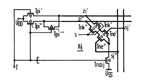
FIGS. 2, 3 and 4 illustrate how the pairs of matrix
switching elements Ki~ can be realized in circuit-oriented terms.
The pairs of switching elements Kij respectively formed with two
switching transistors Tnk', Tnk " that have their respective
control electrodes charged with a through-connect signal or,
1 3 2 0 2 ~ 9 20365 2945
respectively, inhibit signal and have the main electrode
connected to the ~ne or, respectively, to the other sign~l
conductor zi~, zi~ of the appertaining matrix output line each
respectively comprise two series transistors Tne', Tne" that
respectively form a series circuit with a switching transistor
Tnk' or, respectively, Tnk''. These series transistors
respectively have their control electrodes connected to the one
signal conductor sj' or, respectively, to the other signal
conductor sj'' of the appertaining matrix input line (column
line) sj and the respective main electrode facing away from the
series circuit being connected via a sampling transistor Tna
(namely Tnaij in FIG. 2 or, respectively, Tnaj in FIG. 3 or,
respectively,Tnai in FIG. 4) to the one terminal U5s (groun~) of
the operating voltage source. The signal conductors zi', zi'' of
the respective matrix output line (row line) zi are respectively
connected to the other terminal UDD of the operating voltaye
source via a pre-charging transistor Tpi' or, respectively,
Tpi" . The two pre-charging transistors Tpi', Tpi" l1ave their
main electrodes ~acing toward the respective matrix output line
~zi', zi ") connected to one another via a shunt transistor
Tpi' " whose control electrode is connected to the control
electrodes of the pre-charging transistor Tpi', Tpi".
As also illustrated in FIG,. 2, a respective sampling
transistor Tnaij associated to a pair of swi~c~ling
elements can be provided. Alternatlvely, however, as shown in
FIG. 3, a sampling transistor Tnaj that is shared by all pairs of
switchingelements lying at one and the same matrix input line
(column line) 5j and that, therefore, is associated to a ma~rix
input line can be respectively provided or, as may be seen from
FIG. 4, a sampling transistor (Tnai in FIG. 4) shared by all
~3~2J~
20365-2945
pairs ofswitc~ingelements lying at one and the same matrix output
line (row line) ~i that, therefore, is associated to a matrix
output line can be respectively provided. As may be seen fromFIG-
URE 3, a pre-char~ing transistor Tpaj associated to a matri~: input
line can be provided in addition to a sampling transistor Tnaj
associated to a matrix input line and, as may be seen from FIG.
4, a precharging transistor Tpai associated to a matrix output
line can be provided in addition to a sampling transistor Tnai
associated to a matrix output line.
As also indicated in FIGS. 2-4, given a crosspoint
matrix constructed in complementary-metal-oxide-semiconductor
(CMOS) technology, the switching transistors Tnk, the series
transistors Tne and the sampling transistors Tna can be n-channel
transistors and the pre-charging transistors Tpi can be p-channel
transistors. Opposite one another, pre-charging transistors Tpi
and ~ampling transistors 'rna respectively have their control
electrodes connected with a clock T, as indicated in FIG. 5 at
line T, that ~.ubdivides a bit through-connect time intervc)l into
a pre-charge phase pv and into a main phase ph in the manner
indicated at the bottom of FIG. 5.
During the pre-charge phase pv, as shown at the bottom
of FIG. 5, the two respective signal conductors ~zi', zi'') o~
the matrix output lines (row lines) zi arecharged at least approxi-
mately to the operatiny potential UDD via the respective pre-
charging transistor (Tpi' or, respectively, q'pi " in FIGS. 2-4),
to which end the pre-charging transistors Tpi', Tpi " formed by
p-channel transistors in the present example can be made
transmissive by a "low" clock signal T (see line T, FIG. 5).
With the trailing edge of the clock signal T, the shunt
transistor Tpi " ' lying between the two signal conductors zi',
1 3 2 ~ 2 ~ 9 20365 2945
zi'' thereby also becomes simultaneously conductive, with the
result of a short of the two signal conductors zi', zi'' as a
result whereof a balancing of potential of the two signal
conductors zi', zi'' initially occurs very quickly at the
beginning of the pre-phase (the time tl of FIG. 5, line zi).
Subseq~ently, t~lereto, both signal conductors zi', zi" (ti~at are
now balanced in terms of potential) are charged towards the
operating potential UDD via the two pre-charging transistors
Tpi', Tpi'', whereby the overall charging time is shortene~ in
that both pre-charging transistors Tpi', Tpi'' are now involved
in the charging event after the equalization of potential
produced by the shunt transistor Tpi" '.
Simultaneously with the unlocking of the pre-charging
transistors Tpi', Tpi'' and of the shunt transistor Tpi''', the
transistors Tna (Inaij of FIG. 2, Tnaj in FIG. 3 anc~ lnai in
FIG 4) formed by n-channel transistors are driven in the
opposite sense in the example by the same "low" clock signal T,i.e.they
are inhibited, so that the charging of the respective two signal
conductors (zi', ~i") o~ the matrix output lines ~row lines) zi
2G can proceed independently of the drive o~ the respective
switching transistors Tnk', Tnk " ~in FIGS. 2-4) and o~ the
respective series transistors Tne', Tne " ~in FIGS. 2-4) of the
individual pairs of matrix switching elements Kij. As the lines
sj in FIG. 5 shows, the potential corresponding to the respective
bit to be through-connected can thereby already potentially build
up ~or, respectively, be maintained) on the respective matrix
input line (column line) sj.
When, as shown in FIG. 3, a precharging transistor Tpa;
associated to a matrix input line is provided in addition to a
sampling transistor Tnaj associated to a matrix input line or, as
- 1 3 2 0 2 ~ 9 20365-2945
shown in FIG. 4, a precharging transistor Tpai associated to a
matri~ output line is provided in addition to a sampliny
transistor Tnai associated to a matrix output line, then t~e
pseudo-ground line PM is charged during the pre-charge phase pv
via the pre-charging transistor (Tpaj in FIG. 3, Tpai in FIG. 4)
wherewith the respective pair of matrix switching elements Kij is
unburdened in this respect. Particularly given extensive
crosspoint matrices having a multitude of pairs of matrix
switching elements Kij connected to the pseudo-ground line PM,
this leads to a noticeable shortening of the charging time that,
in turn, fully enters into a corresponding increase in the
wor~.ing speed.
Due to the equality of potential of the two signal
conductors zi', zi" produced by the shunt transistor Tpi''', the
initial conditions for reliable amplification by the differential
ampli~ler ~i (PlG. 1) are established correspondingly ear]y, so
that the following main phase ph (bottom o~ FIG. 5) can already
begin at a corres~ondingly earlier point in tlme. In the present
example, the pre-charging transistors Tpi', Tpi" and the shunt
transistor Tpi " ' ~in FIGS. 2-4) are inhibited in the main phase
ph ~see bottom of FIG. 5) by a "high" clock signal T (see FIG. 5,
line T) ànd the sampling transistors Tna (Tnaij in FIG. 2, Tnaj
in FIG, 3, Tnai in FIG. 4) are simultaneously unlocke~. When the
switchlng transistor6 Tnk', Tnk " ~ln FIGS. 2-~) estahlished in
the example by n-channel transistors, are corlductive in a pair of
matrix switching elements Kij due to a through-connect signal ~a
"high" through-connect signal in the example, as shown in FIG. 5,
line s) applied at the control input s and when, there~ore, the
crosspoint is in its through-connect condition, then, dependent
on the signal states prevailing on the two signal conductors s~',
1 3 2 0 2 ~ ~ 20365-2945
sj'' of the appertaining matrix input line (column line) sj and
corresponding to the bit to be through-connected, the signal
conductors zi', zi'' of the matrix output line (row line) zi
connected to this matrix input line (column line) sj via the
appertaining matrix switching element Kij will now be discharged
or, respectively, will remain at the potential UDD assumed in the
pre-phase pv. When "low" signal state prevails on a sicJnal
conductor sj' or, respectively, sj'' of the appertaining matrix
input line (column line) sj and, correspondingly, the (n-channel)
series transistor Tne~ or, respectively, Tne'' (in FIGS. 2-4) of
the appertaining pair of matrix switching elements Kij i5
inhibited, then the appertaining signal conductor zi' or,
respectively zi " of the matrix output line (row line) zi will
not discharge via the appertaining matrix switching element of
this pair of matrix switchiny elements Kij but will retait1 the
potential U~D state insofar as no other crosspoint leadi.ng to
this matrix output line (row line) zi is situated in the through-
connect condition.
When, by contrast, the "high" siynal state prevails on
a signal conductor sj' or, respectively, sj " which was just
under consideration in the matrix input line (column line) sj
and, accordingly, the series transistor Tne' or, respectively,
Tne " (in FIGS. 2-4) of the pair o~ matrix switching elements Kij
under consideration as well as the switching transistor Tnk' or,
respectively, Tnk" and the appertaining sampling transistor Tna
are conductive, then the allocated signal conductor ~zi' or,
respectively, zi " of the matrix output line ~row line) zi is
discharged via this matrix switching element of the pair of
matrix switching elements Kij and is drawn to the potential Uss.
132~239
The respective input signal is therefore through-
connected in an inverted form via a crosspoint that is unlocked
proceeding from its control input s.
In the exemplary embodiment set forth above with
reference to FIGS. 2-4, the pre-charging transistors Tpi', Tpi''
are formed by p-channel transistors, whereby these p-channel pre-
charging transistors Tpi and the sampling transistors Tna formed
by n-channel transistors are controlled opposite one another by
one and the same signal T as a consequence of the different
channel type. In a departure thereof, however, it is also
possible to realize the pre-charging transistors with n-channel
transistors such that only transistors of one and the same
channel type are employed when the switching transistors (Tnk),
the 6eries transistors ~Tne) and the sampling transistors (Tna)
are also n-channel transistors. So that the pre-charging,
transistors and the sampling transistors are then again
respectively oppositely charged with the switching matrix network
drive ¢lock at their control electrodes, the switching matrix
network drive clock 6ignal ~T), as in the exemplary embodiments
set forth with reference to FIGS. 2-4, is to be directly supplied
to the sampling transistors (Tna) but the inverted switching
matrix network drive clock signal, by contrast, is to be supplied
to the ~n-channel) pre-charging transistors.
Although I have described my lnvention by reference to
particular illustrative embodiment~ thereof, many changes and
modifications of the invention may become apparent to those
skilled in the art without departing from the spirit and scope of
the invention. I therefore intend to include withln the patent
warranted hereon all such changes and modifications as may
reasonably and properly be included within the scope of my
contribution to the art.
14