Note: Descriptions are shown in the official language in which they were submitted.
1320279
The invention relates to a multiprocessor system
including a main processor and a co-processor.
In a conventional multiprocessor system including
a main processor and a co-processor such as a processor
specializing in floating-point arithmetic, the co-processor
is comprised of a plurality of electronic components, such
as integrated circuits (IC's), mounted on a plurality of
circuit boards, so that the internal state of the co-
processor can be observed relatively easily. However,
since IC-related technologies have progressed remarkably in
recent years, a typical co-processor now is fabricated with
one large scale integrated circuit (LSI), making it more
difficult to observe the internal state of the co-
processor.
An object of the invention is, therefore, to
provide a multiprocessor system free from the above-
mentioned disadvantage of the current conventional co-
proceesor.
According to an aspect of this invention, there
is provided a multiprocessor system which includes a co-
processor that executes operations instructed by a main
proceeeor using one or more internal registers incorporated
in said co-pro¢essor, said co-processor comprising mode
dlsplay means indicating one of a ~irst mode and a second
mode in accordance with one of a first request and a second
requeet selectively input from said main processor; and
initialization control means which does not initialize said
one or more internal registers when said mode display means
indicates said first mode at the time of completion of each
of eaid operations, and initializes said one or more
internal registers when said mode display means indicates
said second mode at the time of completion of each of said
operatione.
According to another aspect of the invention,
there is provided a process performed by a multiprocessor
system comprising the ~ollowing steps: checking a request
'~'
1320279
line between a main processor and a co-processor to
determine whether a main processor instruction sent from
said main processor to said co-processor is a mode-setting
instruction or a mode-resetting instruction; setting a
debugging mode flag register in said co-processor if said
main processor instruction is said mode-setting instruction
or said mode-resetting instruction; determining if said
main processor instruction is a register dumping
instruction if said main processor instruction is not said
mode-setting instruction or said mode-resetting
instruction; storing contents of internal registers in said
co-processor in a saving area of a main memory if said main
processor instruction is a register dumping instruction;
and executing said main processor instruction as an
arithmetic instruction and clearing said internal registers
if a debugging flag is in an OFF state if said main
processor instruction is neither said register dumping
instruction nor said mode-setting instructions or said
mode-resetting instruction.
Some embodiments of the invention will now be
de~cribed, by way of example, with reference to the
accompanying drawings, in which:
FIG. 1 i~ a block diagram of an example of
conventional multiprocessor systems;
FIG. 2 is a block diagram o~ an embodiment of the
invention; and
FIG. 3 is a flow chart for explaining an
operation o~ the embodiment.
In order to facilitate understanding of the
invention, de~cription will be first provided concerning a
conventional multi-processor ~y~tem.
Referring now to FIG. 1, a conventional multi-
proces~or syetem comprise~ a main processor ~not shown),
~our co-proces~or circuit boards 121 to 124 constituting
one co-proce~sor that operates in accordance with a
microprogram, an external bus 101 connected to the main
proce6~0r as well as the circuit boards 121 to 124, an
132~27~
interface bus for debugging 102 connected to the circuit
boards 121 to 124, and a circuit board for debugging 103
connected to the bus 102. When an instruction is received
from the main processor, under control of the microprogram
the co-processor receives data from the main processor
through the external bus 101, and then processes the data.
Upon completion of the processing, the co-processor
transfers its internal state information, that is, the
contents of its various internal registers (which are
located dispersively on the boards 121 to 124) to the
circuit board 103 via the bus 102. In this manner, the
internal state information of the co-processor is collected
on the ~ircuit board 103.
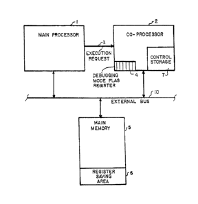
Referring to FIG. 2, an embodiment of the
invention comprises a main processor 1 such as a general-
purpose microprocessor, a co-processor 2 which is
internally provided with a debugging mode flag register 4
and whose operation is controlled by a microprogram stored
in a control storage 7, a main memory 5 having a saving
area 6 for saving the content~ of internal registers of the
¢o-proces~or 2, an external bus 10 connecting both of the
proce~or~ 1 and 2 to the main memory 5, and an execution
reque~t line 11 transmitting instructions from the
processor 1 to the co-proces~or 2.
The co-proce~sor 2 performs operations in
accordance with the operation flow shown in Fig. 3 under
control of the microprogram. The operations will next be
de~cribed in detail.
It is assumed that the processor 1 first is~ues
a mode-setting instruction which is tran~mitted to the co-
proces~or 2 via the line 11 ~step Sl).
The co-processor 2 first examines whether the
instruction received from the line 11 is any one of a mode-
~etting in~truction and a mode-resetting lnstructlon ~Step
S2). Since the instruction received is for setting a
debugging mode, a debugging mode flag stored in the
debugging mode register 4 which is usually kept in an OFF
B
i32027~
state is turned into an ON state (Step S7). After turning
the mode flag into the ON state, the processor 2 waits for
a subsequent instruction (Step Sl). Then, when the co-
processor 2 receives an instruction for an arithmetic
operation from the processor 1, the processor 2 checks to
see whether or not the instruction received is any one of
a mode-setting instruction or a mode-resetting instruction
(Step S2). Since the instruction received is neither the
mode-setting instruction nor the mode-resetting
instruction, the processor 2 next examines whether the
received instruction is a register-dumping instruction
(Step S3). If not, the processor 2 performs an arithmetic
operation specified by the received instruction (Step S4)
because the received instruction is not a register-dumping
instruction. After completion of the execution of the
instruction, the processor 2 checks to see if the mode flag
is in the ON state. If at (Step 5) this time, the mode
~lag is in the ON state, the processor 2 waits for the next
instruction without initializing its internal registers.
Then, when the processor 2 receives a register-dumping
instruction from the processor 1, the processor 2 examines
whether the instruction received is a register-dumping
in~truction a~ter it executes the operation at Step S2.
Since the received instruction is a register-dumping
instruction, the processor 2 stores the contents of the
internal registers into the saving area 6 o~ the main
memory 5 (Step S6) and then waits ~or a subsequent
in~truction (Step S1). A~ter completion o~ the execution
o~ the register-dumping instruction, the processor 1 issues
a mode-resetting instruction to the processor 2 which then
per~orms the above-mentioned judgement operation at Step
S2. Since the instruction issued is a mode-resetting
instruction, the processor 2 turns the mode Plag into the
OFF ~tate and then waits for the next instruction.
The debugging mode ~lag is usually kept in the
OFF state, and the internal registers are usually
initialized (Step S8) whenever an arithmetic operation
132~79
specified by an arithmetic instruction given from the
processor 1 is completed. Such initialization allows the
processor 2 to start execution of the next instruction as
soon as possible.
While this invention has thus far been described
in conjunction with the preferred embodiment thereof, it
will now readily be possible for those skilled in the art
to put this invention into practice in various other ways.
~0