Note: Descriptions are shown in the official language in which they were submitted.
~32~3~
CARDIAC PACEMAKER WITH SWITCHED CAPACITOR AMPLIFIERS
BACKGROUND OF THE INVENTION
The present invention relates generally to artlficial
cardiac pacemakers, and more particularly to an implantable
bradycardia pacemaker having switched capacitor ampli~ier
circuits for various functions, including sensing of cardiac
activity, providing a voltage reference in conjunction with
such sensing, and voltage regulation.
In the normal human heart, the sinoatrial (S-A~ node
is the primary natural pacemaker by which rhythmic electrical
excitation is developed. The cardiac impulse generated at
the S-A nodc is transmitted to the atrial chambers at the
right and left sides of the heart. In response, the atria
contract, pumping blood from those chambers into the
respective ventricular chambers. The impulse is transmitted
to the ventricles through the atrioventricular ~A-V) node,
which imposes a delay, and via a conduction syste~ comprising
the bundle of His, the right and left bundle branches, and
the Purkinje fiber~. In response, the ventricles contract,
the right ventricle pumping unoxygenated blood through the
pulmonary artery to the lungs and the left ventricle pumping
oxygenated (arterial) blood through th~ aorta and the lesser
arteries to the body.
The right atrium receives the venous ~unoxygenated)
blood from the upper part of the body (head, neck and chest)
~3~33
via the superior vena cava, or upper great vein, and from the
lower part of the body (abdonen and leg~) via the inferior
vena cava, or lower great vein. The blood oxy~enated by the
lungs is carried via the pulmonary veins to the left atrium.
This action is repeated in a rhythmic cardiac cycle
in which the atrial and ventrlcular chambers alternately
contract and pump, then relax and fill. One-way valves along
the vein~, between the atrial and ventricular chambers in the
right and left sides of the heart (the tricuspid valve and
the mitral valve, respectively), and at the exits of the
right and left ventricles (the pulmonary and aortic valves,
respectively~ prevent backflow of the blood as it moves
through the heart and the ci-culatory system.
The S-A node is spontaneously rhythmic, and the
normal cardiac rhythm originating therefrom is termed sinus
rhythm. Disruption of the natural pacemaking and propagation
system occurs as a result of aging or disease, and is
commonly treated by artifioial cardiac pacing. The
artificial pacemaker is implanted to deliver rhythmic
electrical to the heart as necessary to effect stimulation at
the desired rate. Bradycardia pacers are designed to sense
cardiac activity at a rate lower than the normal sinus rate
range, and to return the rate to a selected value within that
range. In its simplest form, the pacemaker consists of a
pulse generator powered by a self-contained battery pack, and
a lead including at least one stimulating electrode
~ 3 2 ~ 3 3 ~
electrically connected to the pu15~ gen~rator. The lead is
typically o the catheter type for intravenous insertion to
position the stimulating electrode for delivery of electrical
impulses to excitable myocardial tissue in the appropriate
chamber at the right side of the patient's heart. Usually,
the pulse gcnerator i9 surgically implanted in a subcutaneous
pouch in the patient's chest. In operation, the electrical
stlmuli are delivered to the exc~table cardiac tissue via an
electrical circuit that includes the stimulating and
reference electrodes and the body tissue and fluids.
Typically, the pacemaker is designed to operate in
one of three different response modes, namely, asynchronous
(fixed rate), inhibited (stimulus generated in absence of
specified cardiac activity), or triggered (stimulus delivered
in response to speciPied cardiac activity). The demand
ventricular pacemaker has been the most widely used type,
sensing the patient's natura:! heart rate and applying stimuli
only during periods when that rate falls below the preset
pacing rate.
Pacemakers range fro~ the simple fixed rate devlce
that provi~es pacing with no sensing function, to the highly
complex model implemented to provide fully automatic dual
chamber pacing and sensing functions. The latter type of
pacemaker is the la~est in a progression toward physiologic
pacing, that is, the mode of artificial pacing that restores
cardiac function as much as F,ossible toward natural pacing.
~ ~Qci3~
In V.S. patent No. 4,880,004 of Baker et al.,
titled "Implantable Cardiac Stimul.ator with Automatic Gain
Control and Bandpass Filtering in Feedback Loop" (Attorney's
Docket No. 046/077, assigned to the same assignee as is the
present application, a cardiac stimulator is disclosed in
which the electrical signal representative of detected cardiac
activity is subjected to automatic gain control and bandpass
filtering. The resulting signal is processed for comparison
with inner and outer targets, or refPrence levels, to
determine of the nature of the cardiac activity and ultimately
to correct abnormalities in that activity. The device
described in the Baker et al. application is primarily
concerned with tracking rapidly vaxying signals of the type
commonly associated with fibrillation, in which the heart
undergoes random contractions of individual tissue sections
rather than coordina~ed contraction of the entire mass of
tissue of the chamber. The device locks in on the signal,
changing signal gain as necessary to track the signal, toward
delivering a therapy suitable to return the heart to ncrmal
cardiac activity. The filtered and amplified signal is
compared with inner and outer targets and the gain is varied
according to target crossings.
It is a principal cb~ect of the present invention to
provide a bradycardia pacemaker which utilizes a switched
capacitor amplifier and comparator system to sense abnor~al
cardiac activlty and stimulate the he~rt accordingly.
Another object of the present invention is ~o provide
highly stable voltage re!feIenc~ levels, using switched
capacitor amplification, as targets for comparison with ~he
level of the cardiac signal.
Yet another objec:t o~ the invention is to provide
stable regulation of the supply voltage for the pacemaker,
utilizing switched capacitor a~plification.
SUMMARY OF THE INVENTION
According to the present invention, a pacemaker sense
amplifier which differs from the traditional forms is
employed to detect evoked potentials. In particular, the
sense amplifier comprises a switched capacitor amplifier
which allows the amplifier's bandpass frequency and gain to
be selectively adjusted, and a dual comparator switched
capacitor amplifier system in which each comparator is
multiplexed to provide two target reference levels each for
comparison against the gain and frequency selected dete~ted
signal representative of cardiac activity. If a comparator
is tripped as a consequence of the input signal level
exceeding the selected target level, the pulse generator of
the pacemaker is instructed to pace. On occasions when the
target level exceeds the input signal level, the pulse
generator is inhibited.
The voltage reference from which the target levels of
~ 3 ~
the comparators are derived also utilizes a switched
capacitor aMplifier according to the invention. The
amplifier is switched in a manner to detect and amplify input
levels that are sensitive to temperature in opposite
directions such that the sensitivity is cancelled out in the
ampli~icat$on and a ~ubsequent sample and hold opera~tion.
The resulting voltage reference level is converted to a
reference current which i~ independent of supply voltage and
other circuit componen'ts, to Purther stabilize the output
voltage reference.
According to anot:her feature of the invention, a
volta~e regulator is provided which also employs a
multiplexed multi-target single comparator to selectively
compare and thereby control the level to which the output
pacing capacitors of the pacemaker are charged, and the level
selected as the end of service battery voltage of the
pacemaker~
BRIEF DESCRIPTION OF THE DRAWINGS
The above and other objects, aspects, features and
advantages of the present invention will become more apparent
from a consideration of the ensuing detailed description of a
presently preferred embodlment thereof, taken together with
the accompanying drawings, in which:
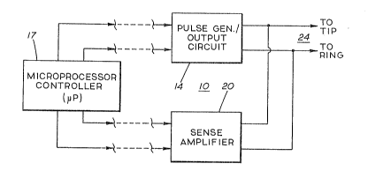
FIG. 1 is a simplifed block diagram of the overall
cardiac pacemaker including a microprocessor-controlled sense
~ 32~
amplifier according to the invention;
FIG. 2 is a schematic circuit diagram of the
preferred embodiment of the sense amplifier of FIG. 1;
FIG. 3 is the ga:~n--frequency characteristic of the
variable gain stage of the circuit of FIG. 2;
FIG. 4 is a timin~ diagram for the comparator stage
of the amplifier circuit of FIG. 2;
FIG. 5 i5 a diagram showing the voltage reference
targets for an exemplary portion of a cardiac signal;
FIG. 6 is a schematic circuit diagram of the
preferred embodiment of the invention utilized to provide the
voltage reference for the circuit of FIG. 2; and
FIG. 7 is a schematic circuit diagram of an exemplary
embodiment of a voltage regulator for the pacemaker according
to a preferred embodiment: of the invention.
D AILED DESCRIPTION OF THE P EFERR.D EMBODIMENT
Referring now to FI~. 1, a cardiac pacemaker 10
comprises an output circuit 14, a mlcroprocessor controller
1~, and a sense amplifier 20. ~ith bipolar operation, for
example, a pair of electrodes may be coupled to output
circuit 14 and sense amplifier 20 via a lead assembly 24 for
pacing and sensing functi.ons. The output circuit 14 is of
any conventional type for generating stimulating pulses which
are to be selectively deliverld (depending on the specific
nature of the pacemaker, such as fixed rate, inhibited or
3 ~
triggered) to the heart of the pacemaker patient, via the
stimulating cathodic electrode of lead assembly 24 and
through the return path of the body tissue and fluids and the
indifferent anodic electrode. Output circuit 14 is also
conventionally implemented to be controlled by microprocessor
l~. For example, the microprocessor may be used to control
the amplitude and width of each stimulating pulse, and the
timing of the discharge of 01ltpUt capacitors of the output
circuit following charging to a desired energy level directly
from the pacemaker batteries or Prom a multiple of the
battery output.
According to the invention, sense amplifier 20, which
includes several stages, pro-~ides automatic gain control and
voltage comparisons by means of switched capacitor
amplifiers. The automatic gain control feature of the
invention is provided utilizlng a low current, low voltage
switched capacitor amplifier with good transient response.
Referring to FIG. 2, amplifier Al i'3 a conventional input
stage for amplifying and filtering the slgnal representative
o~ cardiac activity ~f the patient in whom the pacemaker is
implanted. The signal is obtained at the tip and the ring
inputs 30 of the implanted pulse generator section which is
electrically connected to the sensing electrodes of the
pacing lead 32. Blankin~ switches serve to disconnect the
~nputs during pace. The output signal of amplifier stage Al
is applied to a variable gain stage A2 comprising a switched
capacitor high-p~ss ampl~fier 35, and a plural~ty of switches
~ 3 ~
driven by non-overlapping clock phases. A capacitor CF is
connected in a feedback loop for the amplifier. The other
capacitor with associated switches is the equivalent- circuit
of a resistor.
The microprocessor programs the switches associated
with an array ~0 of parallel capacitors, for selective
electrical connection of capacitors in the array in parallel.
The ratio of the capacltors in array 40 is binary weighted,
such that capacitor 41 is C, capacitor 42 is 2C, capacitor 43
is 4C, and so forth, the effective capacitance being CT
(Ctotal). The flat band gain of the stage is equal to Ctotal
over CF (CT/CF)~ which provides gain control. The effect i~
a variable gain stage which may be written into by the
microprocessor to provide the desired capacitance values, and
thereby the gain. The output signal of stage A2 is a further
filtered and amplified version of the cardiac signal. A
subsequent amplifier stage A3 may be employed to provide
additional gain, if desired.
The value of unit capacitor Cu, adapted to be
selectively connected in the ~eedback path of amplif ier 35,
is significant in tha~ it aids in determining the gain versus
frequency characteristic (FIG. 3) of variable gain stage A2.
In particular, the ratio o~ C~r and CF together with the unit
capacitor and the clock used to set the switches determine
the corner 50 of the gain-~requency characteristic. The
amplifier stage A2 blocks DC, and at a selected frequency the
3 3 ~
ampll~er prOvldes 9ignal ~aln. At the h~gh frequencles of
the f~at band (~B) reglon of the ampl.ifier, the signal ~s
sub~ected to a relatlvely c~nstant galn AFB equal to CT/CF.
Referrln~ agaln to FIG. 2, the output 9i~nal of A2
(or A3, if us~d) is fed to a comparator stage 55 whlch look5
at th~ amplltude of th~ l~com~n~ nal and compares it to a
scaled volta~e r~ference- If the amplltude of the incoming
~ignal ~rom the varlable yain ~tage A2 ls greater than the
level of the voltage reference, the comparator generates a
logical output. This indicates that the signal amplitude is
sufficiently large and is sensed, and informs the rest of the
logic of the action to be taken.
The system of the present ~nvention differs from the
AGC/bandpass and comparator system of the cardiac ~tl~lator
disclosed in the aforementioned U.S. patent No. 4,B80~004
application in, among other things, the syste~ by which ~ain
change is effected, comparators are sequenced and targsts are
created for comparison with the incomin!~ signal. In the
present invent~on the use of switched capacitors allows time
divlsion. In particular, in the ~ult~-tar~et dual comparator
stage 55, each of two comparators ~8 and 59 is ~ultiplexed to
provide four targets, or voltage reference levels, wlth two
targets provided by each set o~ comparators. Co~parator 59
is identical to comparator 58, except that the latter is used
for establishing and measuring signal voltages and target
levels above analog ground whereas the former perorms that
~ 3
function below analog ground.
Referring also to the timing diagram of FIG. 4, the
basic comparator 58 operates wlth two phases consisting of an
auto zero (AZJ phase and a measure (M) phase. The phasing
for the switches associated with each comparator is indicated
by the A~ and M labels. In one phase the amplifier is auto-
zeroed to charge the capacitors C1 and G2 of comparator 5~.
Capacitor C2 is connected to VDD, and capacitor C1 is
connected to the input of the comparator stage. Then,
immediately prior to the next phase, the measure phase, those
capacitors have been charged such that one is relative to
analo~ ground and the other has the input voltage stored on
it away from analog groulld. Additionally, they also have the
offset voltage of the amplifier stored on them. In the
measure phase, capacitor C1 is switched to the analog ground
point (VAG), and capacitor C2 is switched to VREF~ and
therefore the .input signal voltage to the comparator relative
to the analog ground po~nt will trip the comparator if that
voltage is ~ufficiently above (or below) analog ground. The
comparator stage 55 may be viewed as looking at signal levels
about analog ground that have been scaled by the ratio
Cl/(Cl+C~).
In each auto-~ero phase, C1 i8 charged to Vin and C2
is connected to VDD, as well as to store the offset voltage.
In the following phase, C2 is switched to V~EF and C1 is
switched to VA~. If the voltage on C1 does not change, the
~2~
voltage seen by the comparator would decrease by an amount
equivalent to the ratio C1/~C1 ~ C2J. If the voltage on C2
does not move, the signal level seen by the comparator would
increase. In essence, the comparator is reading Vin relative
to VD~, and V~EF relative to VAG~ and subtracting the two
readings. The comparator is utilized to create the zero
point and to store all voltage off5ets. The VREF to VDD
excursion i5 always the same, and sets a target ~in this
instance, an inner or lower target) constituting a threshold
level based on the ratios of the capacitors (here, C1/C2).
When Vin is moved up toward ~JAG in the measure phase, if the
voltage at the node being me~sured returns to become equal to
that excursion, the comparator will be tripped.
The upper (or outer) target is established and the
input voltage lsignal level) is compared against it in a
similar manner using capacitor C3 in place of C2. C3 is
connected to V~D during the auto-~ero phase by the ~witch
selection as shown in the timing diagram, at the same tlme
that C1 is connected to the comparator ~tage input node.
Then, in the following measure phase, C1 ls ~w~tched to
analog ground and C3 i~ switched to the voltage reference.
The upper target is therefore establi~hed accordi~g to the
ratio Cl/C3. The relat~onship of the various volta~s and
5ignal levels and the target levels in the comparator stage
55 is shown in FIG. 5.
Referring now to the timing diagram of FIG. 4, there
12
~ 3 ~
are two phases of the clock, the auto-zero (AZ) phase and the
measure (M) phase. The select (SEL) clock selects the phase
to provide multiplexing. The M phase actually strobes the
value to be latched in at the point indicated on the measure
cycle, as shown by the arrows in FIG. 4, to select which
target (lower or upper) is to be used as a thre~hold level at
a particular point in the cycle.
In one auto-zero/measure cycle, capacitor C3 is in as
a result of 'the switching produced by the SEL and Mu (M
upper) clock. In the next auto-zero/measure cycle, capacitor
C3 is out and capacitor C2 is in as a consequence of the
switching produced by the SEL and ML (M lower) cloc~. The
clock designated M in FIG. 4 is merely a composite of the M
upper and M lower clocks. The e~fect is an alternating of
the upper and lower targets, with the upper target being
latched in during one auto-zero/measure cycle and the lower
target being latched in during the next cycle. Hence, a
single comparator is multiplexed to provide two different
targets.
The target will either be tripped or not, depending
on the magnitude of the input signal. Comparator 58
determines the relative magnitudes of the input signal and
inner and outer targets above analog ground, and comparator
59 does the same with respect to the input signal and targets
below analog ground, as shown in FIG. 5. The two comparators
are non-overlapping; that is, both are never high or low at
13
~ 3 ~
the same ti~e which i~ an important aspect of the
comparison. On one cycle, the clock signal i5 applied to a
switch such that the amplifier is auto-zeroed. The voltages
stored on the capacitors are then measured, and, depending on
the ma~nitude of the stored volta~es relative to the
reference voltage, the target is either tripped or not. On
the next cycle the amplifier is auto-~eroed, the measurement
of stored voltage versus voltage reference is taken, and the
switch is .left open.
It will be observed, then, that the capacitor C3 is
connected into the circuit on every other cycle. On the
cycle that capacitor C3 is in, another target i5 provided.
The same ratio is presented against capacitor C1, but on one
phase C3 is in and on the ne~t phase C3 is out. The result
is that two different targets are provided, but not at the
same time. The sequence is auto-zero, measure, one
capacitor; then, auto-zero, measure, second capacitor. In
the long term, there are effectively two targets. In
reality, ~he same amplifier is being multiplexed to provide
two targets. This is achieved by the addition of capacitor
C3 and the associated switch.
The logic circuit 63 includes latches to lock in the
information at the end of each measure cycle. A relatively
simple OR gati~g circuit wi~l suffice, with latching based on
the application of the M upper and M lower phases of the
clock (FIG. 4) coincident with an output from the respective
14
~32~3~
OR gate. The amplifier is auto-zeroed to remove any offset
voltage, the capacitors are charged, the amplifier is allowed
to settle out, and the information is loc~ed in. By that
time this comparator is either high or low, depending upon
whether the input voltage to the comparator was sufficiently
large to trip the target. At that point in time, the answer
is latched in and supplied to the logic circuit. As a
consequence of the multiplexing of the t~o comparators, four
targets are provided. The output bits are indicated as Vu
(upper) and VL (lower), and indicate whether an upper target
or a lower target was tripped (that is, exceeded by the
magnitude of the signal into the dual comparator stage) and,
if so, which target speclfically. The two targets are scaled
two to one in the presently preferred embodi~ent of the
invention, although that is not essential and a different
ratio may be used if desired.
Referring now to FIG. 6, the circuit employed to
provide the voltage reference from which the various targets
are derived has three main components. The first, in bloc~
80, is a diode array in conjunction with a switched capacitor
amplifier having auto-zero an~ measure phases. DiPferences
in diode voltages are utilized together with the amplifier to
create a signal constitu~ing ~ voltage reference which, at
least on first order, is independent of temperature. The
second ma~or component is a s~mple and hold circuit 85 which
holds the final result. It ignores the auto-zero phase and
~ 32~3~
provides sample and hold to hold the final answer, and also
buffers for outside use. The voltage reference signal is
available at the output circuit of the amplifier 88. To make
the final answer insensitive to other circuit components to
the extent feasible, a current is created from the voltage
reference to produce a suppl~-independent current reference
92 to drive the diodes.
The switched capacitor amplifier is initially i~
auto-2ero mode. Capacitor C5 is thereby connected across the
ampli~ier input (by actuation of switch 94) to store the
offset voltage, and thereby E~utting the amplifier in unity
gain. All ten of the diodes D1 are coupled in parallel and
are turned on to allow current flow through all of them when
switch 96 is on. Each of diodes D1 is of the same emitter
size as the others. For any diode, the voltage across it is
a function of the current flowing thro~gh it. By way of
example, the DC value may be approximately 0.5 volt with a
given current level. But if two diodes have the same emitter
area and the same fixed current flows through them, the total
voltage in the previous exam~le will drop by 18 millivolts.
This is a function of the emit~er size and the current
flowing though it -- the area of the device. So voltage is a
function of the current through the diode and the area of the
device.
The ten diodes are identically the same, for ratioing
purposes. Instead of making one ten times larger than the
1~
~ 3~,~r~3,~
other, better ratioing is achieved by using ten identlcal
diodes Dl ratioed to D2. During the auto-zero phase, the
voltage produced by the current through diodes Dl and diode
D2 is approximately VBE ~base-to-emitter) which, for example,
may be about half a volt. It should be noted that the diodes
are appropriately connected transistors for devices fabri-
cated in CMOS, which is preferred, At this point, however,
the amplifier 99 is in the auto-zero phase also, with
switches 94 and 98 closed, and capaci~ors Cs and C6 are being
charged to the offset voltage. Hence, the amplifier 99 does
not see VBE as an input voltage.
During the next phase, the measure phase, the auto-
zero switches are open and switch 101 is closed to put
capacitor Cs back in the feedback circuit of the amplifier,
with the offset stored on it. Amplifier 99 is again
available to a~plify signal appearing at its input, and the
amplification will take place according to the ratio of those
capacitors, c6/cs. The incremental input voltage to
amplifier 99 is now delta VBE, since diodes Dl have been
removed ~rom the current path, and whatever current flow
exists is through diode D2. Thus, for example, if the
voltage at the input node to the amplifier were 0.5 volt when
the large current flowed through the diodes Dl path, the
voltage is now considerably .ess than that (delta VBEJ, and
will be amplified. Consequently, the final voltage is VBE
[(C6/C5) x delta VBE]. That is the answer stored by the
~32~
samp~e and hold circuit 88 when, at the end of the measure
phase, switch 104 is closed.
Voltage VBE obtained with current flow through all of
the diodes D1 and D2 decrease~s with temperature, but delta
VBE which is obtained from t~le ratioed difference in current
~low, increases with temperature. The increase of the latter
is less than the decrease of the former for any given
temperature increase; hence, it is necessary to amplify the
differential temperature coefficient to produce a voltage
with substantially zero temperature coePficient. In the
presently preferred embodiment of the voltage reference
circuit, that voltage is the band gap of silicon, and the
circuit is essentially a band gap voltage amplifier for
providing the voltage reference.
As noted above, it is important that the voltage
reference be made independent not orlly of temperature, but of
supply voltage as well. To that encl, the voltage Yref
resulting from the sample and hold operation is fed back to
provide a current reference by means of the circuit 92. The
current through resistor 107 (RbiasJ is Vref/Rbias, which can
be ratioed by means of the transistors 109, 110 to control
the current flow at the diode array, and provides the desired
stability.
Referring now to FIG. 7, a voltage regulator circuit
suitable for the sense amplif:ier comprises a switched
capacitor two input comparator 125, which operates in the
1~
~ 3 2 ~ ~ 3 ~
manner described for a single comparator in the sense
amplifier of FIG. 2, except that the comparator of FIG. 7 has
flve extra capacitors in an array 129 instead of a single
capacitor. The capacitors in array 129 are binary weighted
to provide 32 different trip points, depending on values that
may be programmed in from the microprocessor.
As in the exemplary comparator described with
reference to FIG. 2, comparator 125 i5 multi-target by means
of multiplexing. The circuit of FIG. 7 is used in the
presently preferred embodiment of the invention to regulate
the amplitude of the voltage on the capacitors 132 that
supply the pacing outputs to the pacing lead and electrodes.
The voltage regulator circuit is also utilized to measure Vss
and to co~pare it to the voltage reference to ascertain when
the supply level is at end of service (EOS), or at a point
now more often referred to as initial followup indicator
(IFI) or elective replacemen1: indicator (ERI). Basically,
the indication obtained by vi.rtue of this monitoring and
measurement is that the batteries of the pacemaker.are
sufficiently depleted to require replacement.
The voltage regulator also employs conventional
multiplier and logic circuitry with a pair of pumping
capacltors 138. This provides DC to DC conversion in which
the battery voltage is pumped to a multiple thereof for
charging the pacing output capacitors 132. During pacing,
the latter capacitors are discharged, and thereafter must be
19
~32~ $
recharged for ~he next reguired pace. During tha~ cycle, the
logic circuit selects the sw~tching operation of the switches
associated with the comparator to allow ~onitoring by the
comparator. When the desirecl target voltage (determined by
compari~on with the selected reference voltage) is reached,
the comparator ls tripped and charging of the output
capacitors 132 is ceased.
For the ~OS indication, the somparator u~es a tar~et
voltage appropriate for indic:ating elective replacement of
the pulse generator (the batteries) by the patient's
physician. Circuit segment 143 may be laser trimmed for the
selected EOS voltage. The capacitor array provides gain
control ~or the comparator so that, depending on the
programming of the switches by the microprocessor, a wide
array of regulated outputs i5 available for EOS, as well as
for regulation of the charging le~e:i of the output
capacitors.
Although a preferred embodiment of the invention has
been descr.ibed, it will be apparent to those skilled in the
field to which the invention pertains from consideration of
the disclosure herein that various changes and modifications
may be made to the disclosed embodiment without departing
from the true spirit and scope of the invention. Accordingly,
it is intended that the invention be lim.ited only to the
extent required by the appended claims and applicable rules
o law.