Note: Descriptions are shown in the official language in which they were submitted.
1 320~6~
1 BACKGROUND OF THE INVE~ITION
This invention relates to a tracking error
signal forming circuit and a method for obtaining a track-
ing error signal, in particular by using a reproduction
time difference between signals reproduced by at least ~t
heads having different azimuthal angles.
In a recording/reproduction apparatus, e.g. a
magnetic recording/reproduction apparatus (hereinbelow
called simply VTR), etc., when information signals record-
ed on a recording track are reproduced, the trackingcontrol is necessary in order that the play back head
reproduces the recorded signals by scanning just on the
recording track.
As a method utilized in practice for the
tracking control there is known a method, by which a track
exclusively used for the tracking control is disposed
along the longitudinal direction of the tape, in which
control signals are recorded with the frame period on a
period, which is an integer times as long as it, at the
recording of image signals and the tracking control is
efected by using these control signals at the reproduc-
tion. However, this method has a drawback that the track
exclusively used for the tracking control is necessary and
that it is impossible to obtain tracking error signals
over the whole region of the recording track.
~k
1 320568
1 As another method used in practice there is
known a method, by which pilot signals for the tracking
control are recorded on the recording track and at the
reproduction tracking error signals are obtained by
comparing reproduction lavels of the pilot signals repro-
duced from each track adjacent to the main track, which
the head is scanning and reproducing. According to this
method, since it is possible to obtain tracking error
signals over the whole region of the recording track, when
the play back head is mounted on an electro mechanical
converting element constituted by a piezo-electric
element, etc. and the mechanical position of the head is
varied by using the tracking error signals described
above, it is possible to construct a control system
capable of following bending of the track. However this
method has a drawback that, since it is necessary to
record the pilot signals, superposing them on the
information signal, the bandwidth of the information
signal is is reduced by the bandwidth corresponding to
that of the pilot signals and therefore S/N of the
information signal is worsened correspondingly.
In order to remove these drawbacks, ~ method has
been proposed, by which the tracking error signals are
obtained over the whole region of the recording track
without using pilot signals. The method is disclosed in
JP-A-55-150129 and by the method the ~ ~between the
track deviation and the reproduction time difference
f~vO
between reproduced by at least ~ heads having different
1 320568
azimuth anc31es is used. Since this invention relates to
the metllocl, fulldamental conception of the method will be
explained helow.
In the following discussion reference will be made
to -the accompanying drawings in which: -
Fig. l is a scheme showing the relation betweena magnetization trajectory and a pair head;
Fig. 2 is a scheme for explaining the conception
of a method for dividing the signal, when tlle pair head is
used;
Fig. 3 shows the relative positional relation
between the recorded maynetization trajectory and a
playback head:
Fig. 4 shows variations o~ the tracking error
signal in the state where the pair head is mounted
correct]y;
Fig. 5 shows various mounting states of the
heads;
Fig. 6 shows the relative positional relation
between a magnetization trajectory recorded by using a
pair head in the state where the heads are mounted incor-
rectly, and a play~back pair head in the state, where the
heads are mounted also incorrectly:
Fig. 7 shows variations of the tracking error
signal, when a pair head in the state, where the heads are
mounted incorrectly, is used;
Fig. 8 shows the relation between the recorded
magnetization trajectory and the head scanning trajectory;
- 3 -
1 32056~
- Fig. 9 shows variations in the output level oE
reproduced signals obtained by the scanniny with the pair
head indicated in Fig. 8 and the time difference between
the reproduced sigllals with respect to time;
Fig. 10 is a block diagram sllowing the construc-
tion of a recording circuit;
Fig. 11 is a block diagram illustrating a first
embodiment oE this invention;
Fig. 12 is a block diagram illustrating in
detail a time difference detecting circuit and a reference
value forming circuit in tlle first embodiment of this
invention;
Fig. 13 indicates signal waveforms at various
parts in the device indicated in Fig. 12;
Fig. 14 is a block diagram illustrating in
detail a maximum value detecting circuit in the first
embodiment of this invention;
Fig. 15 indicates signal waveforms at various
parts in the circuit indicated in Fig. 14;
Fig. 16 shows the relation between the recorded
magnetization trajectory and the head scanning trajectory;
~ ig. 17 shows a reproduced signal obtained when
the head is forcedly displaced;
Fig. 18 is a block diagram showing the construc-
tion of a recording circuit;
Fig. 19 is a block diagram illustrating a second
embodiment of this invention;
Fig. 20 is a block diagram illustrating in
detail a time difference detecting circuit and a reference
value forming circuit in the second embodiment of this
,~ invention;
~ 3a
" 1 32056~
Fig. 21 indicates signal waveEorms at various
parts in the device indicated in Fig. 20;
Fig. 22 is a block diagram illustrating in
detail an on-track state detecting circuit in the second
embodiment of this invention;
Fig. 23 shows a scanning trajectory obtained by
using the head;
Fig. 24 indicates signal waveEorms a~ various
parts in the circuit indicated in Fig. 22; and
Fig. 25 is a block diagram of a circuit for
forming a starting signal, which drives the on-track state
detecting circui-t, in a third embodiment o~ this invention.
Fig. 1 shows magnetization trajectories recorded by
two heads having different azimuthal angles. In the
~igure 101 is a magnetic tape, which is Eorward in the
direction indicated by an arrow 102. 103 and 104 indicate
two heads having azimuthal angles, which are di~ferent
from each other. They scan the tape simultaneously in the
direction indicated by an arrow 105. Such heads, i.e. two
heads, which scan the magnetic tape simultaneously and
have azimuthal angles, which are different from each
other, are called below a pair head. 106 and 107 indicate
head gaps in the head, respectively. Al, A2, A3, ... are
magnetization teajectories recorded by heads having the
same azimuthal angle as the A head indicated by 103 and
Bl, B2, B3, ... are magnetization trajectories recorded by
heads having tlle same azimuthal angle as the B head indi-
cated by 104. The pair of tracks Al, Bl and the pair o~
tracks A2, B2 may be recorded either by a same pair head
or by another pair head. This relation is determined by
3b
_
1 320568
the number of rotations of the rotating cylinder, in which
magnetic heads are integrated, and the number of pair
heads integrated therein, which can be arbitrarily decided
at the design of the device. The signal on each of the
magnetization trajectories, e.g. magnetization pattern of
the horizontal synchronization signal, etc. is recorded
with an angle inclined to the longitudinal direction of
I 320568
1 the track, as indicated by 108 and 109, i.e. an azimuthal
angle.
The method for recording/reproducing information
signals by means of a pair head is efficient, when the
frequency band of the information signal to be dealt with
is great. This is because, since at recording information
signals with a constant head scanning speed, the higher
the recording frequency of the information signal is, the
shorter the wavelength recording it on the magnetic tape
is and the shorter it is, the more difficult the practical
recording/reproduction is, but it is possible to divide
the frequency band of the information signal, the record-
ing wavelength can be set to be substantially long.
Fig. 2 shows the conception, by which the
~.. ~, .. ,~ o
information signal to be recorded is divided into ~ kinds
of signals. Figure 2-a indicates the original signal to
be recorded and Fig. 2-b and Fig. 2-c indicate signals
obtained by dividing the original signalr i.e. real
recording signals supplied to the pair head. The original
~wO
signal is divided in time into Z portions 201 and 202,
e.g. as indicated in the figure, which are elongated in
time as indicated by 203 and 204, respectively. That is,
it is possible to narrow the frequency band, corresponding
to the elongation in time. In Fig. 2, 205, 206, 207, etc.
are timing signals, e.g. horizontal synchronization
signals. Further the method for dividing the original
signal is not restricted to the method, by which the
original signal is divided in time, but a method, by which
- 4 -
~ 320568
1 it is divided in frequency, a method, by which it is
divided, depending on the kind of signals such as the
brightness signal, the color signal, etc., and so ~orth
are conceivable. In any case, in the case where signals
having a wide frequency band are to be recorded, the
method using a pair head is efficient in practice a~d
inevitable.
Fig. 3 shows 3 positional relations between the
recorded magnetization trajectory and the play back
scanning head. In this figure 301, 302 and 303 indicated
by broken lines indicate pair heads, each of which
consists of an A head and a B head. Each of the pair
heads scans a trajectory in the direction indicated by an
arrow 304. Al and Bl are magnetization trajectories
recorded by a pair head and signals indicated by 305 to
310 represent recording positions of horizontal
synchronization signals. The position of the pair head
with respect to the recorded magnetization trajectories is
deviated towards left on the sheet of the Fig. 3-a, on-
track in Fig. 3-b and deviated towards right in Fig. 3-c.
When a recording track is play-back-scanned with heads
having such relative positional relations, even if signals
are recorded at a same timing, they are reproduced with
different timings. For example, in Fig. 3-a, the timing,
where the horizontal synchronization signal 305 is
reproduced by the head A, is retarded with respect to the
timing, where the horizontal synchronization signal 306 is
reproduced by the head B; in Fig. 3-b the reproduction
1 320568
1 timings of the two horizontal synchronization signals are
equal; and finally in Fig. 3-c the timing, where the
horizontal synchronization signal 309 is reproduced by the
head A, is advanced with respect to the timing, where the
horizontal synchronization signal 310 is reproduced by the
head B. Consequently track deviations can be known by
examining the time difference of the horizontal synchroni-
zation signals reproduced by the heads A and B. Further
the signal, for which the time difference is examined, is
not restricted to the horizontal synchronization signal,
but it may be another specified signal. However this
invention will be explained below, supposing that the
specified signal is the horizontal synchronization signal.
Fig. 4 is a graph showing the relation between
the track deviation and the reproduction time difference
between the horizontal synchronization signals reproduced
by the heads A and B, in which the abscissa indicates the
track deviation, the position indicated by 0 being the
on-track position. The direction of the deviation towards
right and left corresponds to the direction of the devia-
tion of the head Witll respect to the recording track on
the sheet indicated in Fig. 3. ~he ordinate indicates the
reproduction time difference between the horizontal
synchronization signals reproduced by the heads A and B
and the timing, where the time difference is 0, corre-
sponds to the on-track position. Further it is supposed
that the direction of the deviation is positive, when the
timing of the horizontal synchronization signal reproduced
I 32056~
1 by the head A is retarded with respect to that reproduced
by the head B. At this time the relation between the
track deviation and the time difference between the
reproduced signals is represented by a line 401. As it is
clear from Fig. 4, if the tracking control circuit is so
constructed that the time difference indicated by the
ordinate tends to be ~, the play back head play-back-scans
the recorded track always on-track.
However the method, by which the tracking
control is efected by detecting the time difference
between the signals reproduced by the pair head, is diffi-
cult, only when the center positions of the head gaps of
the heads A and B are strictly in accordance with each
other, and otherwise it gives ri.se to track deviations.
This will be explained below.
Fig. 5 illustrates 3 mounting states of the
heads A and B. In the figure 501, 503 and 505 indicate
the head A and 502, 504 and 506 show the head B. The
scanning direction of the heads is indicated by arrows
507, 508 and 509. 512, 513 and 514 represent members for
mounting the heads, which are movable members constituted
by piezo-electric elements, etc. The heads A and B are
mounted so as to be deviated fxom each other in the
direction perpendicular to the scanning direction. The
gap in each of the head is indicated by a full line drawn
aslant in each of the heads, as indicated by 510 and 511.
Fig. 5-a shows the correct mounting state, in
which the center points 515 and 516 of the gaps of the
-- 7 --
1 32056~
1 heads are on a line 517r which is perpendicular to the
scanning direction of the heads. That is, there are no
deviations in ~he scanning direction. In a magnetization
trajectory recorded by using such heads signals having a
s same tlming are recorded side by side in the direction
perpendicular to the longitudinal direction of the
recorded track.
Fig. 5-b shows an incorrect mounting state, in
which the heads are mounted so that the center points of
the gaps thereof are deviated by an amount indicated by
518 from each other in the scanning direction. In a
magnetization tra~ectory recorded by using such a head
signals having a same timing are recorded, deviated ky the
amount indicated by 518 from each other in the longitudi-
nal direction of the recorded track.
Fig. 5-c illustrates another mounting method of
the heads, in which the heads are mounted so that the
center points of the gaps thereof are shifted by an
interval 518 corresponding to the recording wavelength of
the horizontal synchronization signal and in addition the
amount of the deviation 519 in the height of the heads
produced by the shift of the head is corrected by a height
correcting member 520. It is well known that it is
possible to locate the recording positions of the hori-
zontal synchronization signals side by side in the longi-
tudinal direction of the recorded track by means of the
heads thus constructed. However, also in this case,
unless the interval 518 is set so as to be precisely equal
1 320568
1 to the wavelength of the horizontal synchronization signal
or a length, which is an integer times as long as the
wavelength, the condition is identical to that explained,
referring to Fig. 5-b.
Fig. 6 shows the relation between the recorded
magnetization tra~ectory and the play back head, in the
case where a magnetization trajectory recorded by a pair
head, in which the mounting positions of the heads are
deviated from each other, is reproduced by another pair
10 head having also deviated heads. 601 and 602 represent
heads A and B, respectively, and 603 and 60~ indicate
recording positions of the horizontal synchronization
signals. The figure shows a state, in which the pair head
scans the recorded track, when it is on track. At this
time the time difference between reproduction timings of
the two horizontal synchronization signals reproduced by
the h`eads A and B corresponds to a difference between
distances indicated by 6n5 and 606. That is, even if the
pair head is on-track, a time difference is produced
between the reproduced signals.
~ ig. 7 shows the relation between the track
deviation and the time difference between the reproduced
signals, in which the abscissa and the ordinate have the
same meanings as those explained for Fig. 4 and 401 is the
characteristic line indicated in Fig. 4. That is, for
this characteristic line the time differenceJ~ corresponds
to the on-track position. On the other hand the charac-
teristic line indicated by 701 is that obtained, in the
1 32056~
1 case where the relation between the heads and the recorded
magnetization track is that indicated in Fig. 6. That is,
~QRd
in this case, the time difference is not ~ at the on-track
position. If the control were effected so that the time
~e~u
difference is ~ at this time, the control system would be
stabilized at the track position indicated by 702.
The mounting precision of the heads A and B is
determined by the mechanical precision at the head mount-
ing and ~luctuations are always produced. Consequently it
can be said that the relation between the recording
position of the signal and the play back pair head is
generally that indicated in Fig. 6. Furthermore, since
the relation between the distances indicated by 605 and
606 in Fig. 6 is different from deck to deck, unless this
problem is resolved, the method disclosed in JP-A-54-57287
cannot be utilized in practice.
SUMMAR~ OF THE INVENTION
The object of this invention is to provide a
tracking error signal forming circuit, by means of which
the on-track position is automatically set, even if the
relation between the recording position of the signal on
the recorded track and the gaps of the play back pair head
is that indicated in Fig. 6.
A tracking error signal forming circuit accord-
2~ ing to this invention comprises at least two heads havingdifferent azimuthal angles and mounted on an electro-
mechanical converting element, means for obtaining a
-- 10 --
1 320568
reproduction time difference between speciEied signals,
each oE ~hich is contained in the reproduced signal
reproduced by each oE the heads, reference val~e Eorming
means for forminy a reference value for the tracking
control, operatiny means for calculating the difference
between the reproduction time difEerence and the reference
value or the sum thereof, displacement means for displac-
ing forcedly the electro-mechanical converting element in
the positive or negative direction, and maximum value
detecting means for detecting the maximum value of at
least one of the reproduced signals at the displacement of
the element, the reference value forming means including
means for calculating the difference between the reproduc-
tion time difference and the fixed reference value or the
sum thereof at the point of time, where the maximum value
of the reproduced signal is obtained by the maximum value
detecting means.
1 320568
Accordingly therefore the invention also provides
a trac]cing error signal forming circuit comprising:
means for obtaining a reproduction time differ-
ence between specified signals, each of which i.s contained
in the reproduced signal reproduced by each of at least
two heads llavillg different azimuthal angles and mounted on
; an electro-mechanical converting element;
reference value forming means for forming a
reference value for the tracking control;
. operating means foe calculating the difEerence
between the reproduction time difference and the reEerence
value or the sum thereof;
maximum value detecting means for detecting the
maximum value of at least one of the reproduced signals;
and
displacement means for displacing forcedly said
electro mechanical converting element in the positive or
negative direction;
wherein said reproduction time difference at the
point of time, where the maximum value of the reproduced
signal is detected by said maximum value detecting means,
is used as the reference value for the tracking control in
said reference value forming means.
- 12
1 32056~
The invention also provides a tracking error signal
Eorming circui-t comprising:
at least two heads having different azimuthal
angles and mounted 011 an electro-mecllanical converting
element;
rneans for obtaining a reproduction time differ-
ence between specified signals, each of which is contained
in tl~e reproduced signal reproduced by each of said heads;
reference value forming means for forming a
reference value for the tracking control;
operating means for calculating the difference
between the reproduction time difference and the reference
value or the sum thereof;
displacelnent means for displacing forcedly said
electro-mechanical converting element in the positive or
negative direction; and
level difference detecting means for detecting a
level difference between reproduced signals at the dis-
placement;
wherein said reproduction time difference at the
point of time, where the value o~ said level difference
between reproduced signals detected by said level differ-
ence detecting means is within a predetermined region is
used as the reference value for the tracking control in
sai.d reference value forming means.
- 13
1 320568
The invention will now be described in more detail, by
way of example and also with referPnce to the accompanying
drawings introduced above.
Before explaining preferred embodiments of this
invention, the fundamental conception of this invention will
be explained.
Fig. 8 shows the relation between the recorded
magnetization trajectory and the head scanning trajectory and
Fig. 9 shows variations in the output level of reproduced
signals obtained by the scanning with the pair head indicated
in Fig. 8 and the time di~erence between the reproduced
signals with respect to time.
In Fig. 8 Al, A2, ... indicate magnetization
trajectories recorded by the head A and Bl, B2,`... indicate
magnetization trajectories recorded by the head B. 801, 802
and 803 represent head scanning trajectories at various
states. In order to know variations in the outpuk level of
reproduced signals, it is sufficient to examine variations in
the output of either one of the heads A and B. Consequently
explanation will be made, supposing that the head scanning
trajectory described above is the scanning trajectory of the
center of the head gap of the head A. 801 represents the
head scanning trajectory, when the head is on-track, and 802
and 803 are head scanning trajectories, e.g. when the tape is
stopped. The head scanning trajectory at the stopped tape is
not always at a constant position with respect to the
recorded track, but it has a positional relation indicated
- 14 -
t 320568
1 e.g. by 802 or 803.
Fig. 9 shows variations in the output level of
the reproduced signals and the time difference therebet-
ween with respect to time during a scanning period 901
from one end to the other in the longitudinal direction of
a recorded track (Fig. 9(c) and (d)). 902 indicates
variations in the output at the scanning 802 with the
head In the figure 9(b) shows the positional relation
between the magnetization tracks A2 and B2 and the play
back heads 906 and 907 at points of time tl, t3, t5 in the
scanning 802 with head. The point of time t3, where the
maximum value 904 of the reproduced signal is obtained, is
the moment, where the head scans the position indicated by
804. At this time the play back heads 906 and 907 are
on-track on the recorded tracks A2 and B2, respectively.
The time difference between the reproduced signals is
indicated in Fig. 9~d) and this reproduction time differ-
ence T at the point of time t3 may be the reference value
for the following tracking control. Further 903 shows
variations in the reproduction output at the scanning 803
with the head. The moment where the maximum value 905 of
the reproduced signal is obtained, is the point of time
where the head scans the position indicated by 805. That
is, it corresponds to the point of time, where the center
of the head gap in each of the heads is on-track on the
magnetization trajectory A2. Consequently, examining the
time difference between the reproduced signals at the
point of time, where the output level thereof is maximum,
- 15 -
1 320568
1 this time difference may be the reference value, when the
head is on-track. The formation of this reference value
is effected by displacing an electro-mechanical converting
element so that the magnetic head mounted on the electro-
mechanical converting element constituted by a piezo-
electric element, etc. traverses the recorded track in the
direction of the width, when the tape is stopped, i.e.
when the mode passes from the stop mode to the normal
reproduction, and by realizing the head scanning
trajectory, as indicated by 802.
Now a first embodiment of this invention will be
explained.
Fig. 10 is a scheme showing the flow of the
signal processing at the recordiny. In the figure the
image signal to be recorded is inputted in a terminal
1001. A circuit 1002 is a recording signal processing
circuit, which effects processings such as conversion of
the frequency band of the original signal into a frequency
band, which can be recorded, etc. 1003 and 1004 designate
recording amplifiers, which supply recording signals to
the head ~ 1005 and the head B 1006, respectively. 1007
represents a circuit driving the piezo-electric element
(not shown in the figure), on which the heads A and B 1005
and 1006 are mounted. At the recording, in order to keep
the displacement of the head to a constant value, it
supplies a constant voltage to the piezo-electric element.
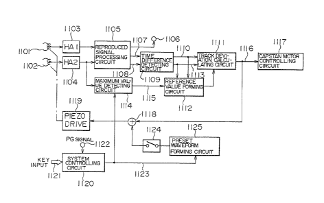
Fig. 11 is a block diagram illustrating the
first embodiment of this invention. A time difference
- 16 -
1 320568
1 detecting circuit 1109, a reference value forming circuit
1112 and a maximum value detecting circuit 1114 indicated
in the figure will be explained later in detail. In Fig.
11, 1101 and 1102 designate the heads A and B, respective-
ly, for reproduction. 1103 and 1104 represent reproduc-
tion amplifiers. 1105 is a reproduction signal processing
circuit, which converts signals reproduced by each of the
heads into the same form as the original signal so as to
be reproduction image signals, which are outputted through
a terminal 110~. Further the reproduction signal
processing circuit 1105 outputs specified signals
reproduced by the heads, i.e. horizontal synchronization
signals 1107 and 1108. The time difference detecting
circuit 1109 is a circuit for detecting the reproduction
time difference between these horizontal synchronization
signals. A signal 1110 corresponding to this time
difference is supplied to the track deviation calculating
circuit 1111 and the reference value forming circuit
1112. The time difference detecting circuit 1109 outputs
the time difference signal and at the same time decides
which one of the horizontal synchronization signals
reproduced by the heads A and B is earlier reproduced and
outputs a polarity judgement signal 1113. A circuit 1114
is the maximum value detecting circuit, which outputs a
signal 1115, whose polarity changes, when the signal
reproduced by the head 1102 is at the maximum value. ~he
reference value forming circuit 1112 forms a reference
value by using the time difference signal 1110 at the
1 320568
point of time, where the polarity oE the signal 11]5
changes. The track deviation calculating circuit 1111
calculates a difference signal between the time difference
signal 1110 supplied by the circuit 110~ and the reference
value supplied by the circuit 1112 and outputs a tracking
error signal 1116. The tracking error signal 1116 is sup-
plied to a capstan motor controlling circuit 1117 and at
the same time to a piezo-electric element driving circuit
1119 through an adder 1118. The capstan motor controlling
circuit 1117 controls the forwarding phase of the tape by
using the tracking error signal 111~. The piezo-electric
element driving circuit 1119 displaces the heads 1101 and
1102 by using the tracking error signal 1116 and effects
the control so as to follow bending of the track. A
circuit 1120 is a system controlling circuit, which output
various kinds of mode instructing signals, depending on a
key input signal 1121. Not only the key input signal but
also a PG signal indicating the rotational phase of the
rotating head through a terminal 1122 are supplied. A
gate signal 1123 outputted hy the circuit 1120 is a
signal, which is at the "High" level only during a
scanning period, where one head play-back-scans one
recorded track, at the reproduction mode. Only during the
period, where the gate signal 1123 is at the "High" level,
the maximum value detecting circuit 1114 works and at the
same time a switch 1124 is closed. A circuit 1125 is a
preset waveform forming circuit. This circuit 1125 is a
circuit for forming a saw tooth signal for driving the
- 18 -
1 320568
piezo-electric element so that the playback hPad traverses
the recorded track, as it has been already explained,
re~erring to FigsO 8 and 9.
Fig. 14 is a block diagram illustrating in detail the
maximum value detecting circuit 1114 indicated in Fig. 11 and
Fig. 15 shows waveforms at various parts in the circuit
indicated in Fig. 14. In the two figures the same reference
numerals represents identical elements.
In Fig. 14 a reproduction signal ~15-b) is inputted
through a terminal 1401. The head scans the recorded
magnetization trajectory in the direction of the width during
the period indicated by 1501 and the reproduction signal (15-
b) indicated in Fig. 15 indicates a reproduction signal
obtained, when the head is on-track and play-bacX-scans the
recorded track during the other period. Such a saanning with
the head is ef~ected by makiny th~ head movable by means of
the electric-mechanical converting element such as a
piezoelectric element, etc. only during the period indicated
by 1501 at the normal reproduction mode. The reproduced
signal (15-b) i~ detected~rectified by a detecting-rectifying
circuit 1402 and transformed into a signal indicated by a
broken line 1502 in (15-c). A circuit 1403 is a peak holding
circuit, which holds the maximum value of the signal 1502 and
outputs a signal indicated by 1503. A gate signal (15-a) is
inputted through a terminal 1407. This gate signal is an
output signal 1123 of the system controlling circuit 1120
indicated in Fig. 11, which is at the "high" level
- 19 -
1 320568
1 only during the period, where the head scans one track, at
an arbitrary point of time at the reproduction mode. The
peak holding circuit 1~03 works during the period, where
the gate signal is at the "high~ level, and the output
signal is at the "Low" level during the period, where the
gate signal is at the "Low" level. A circuit 1404 is a
level comparing circuit, which compares the level of the
output signal 1502 of the detecting-rectifying circuit
with the level of the output signal 1503 of the peak
holding circuit. The comparing circuit outputs a signal,
which is at the "High" level, when the level of the output
signal of the peak holding circuit is higher than that of
the detecting-rectifying circuit ~as indicated in Fig.
15-d) The switching circuit 1405 takes out a signal
(15-d), when the gate signal (15-a) is at the "Highn
level, and it is connected to the ground side during the
"Low~ level period. A timing signal (15-d) forming the
reference value, which will be described later, is taken
out through a terminal 1406.
Fig. 12 is a block diagram indicating in detail
the time difference detecting circuit 1109 and the
reference value forming circuit 1112 indicated in Fig. ll
as well as the tracking deviation calculating circuit
1111. Fig. 13 shows signals at various parts in the
circuit indicated in Fig. 12. Same reference nurnerals in
Figs. 11, 12 and 13 represent same items.
In Fig. 12, a horizontal synchronization signal
(13-a) contained in the signal reproduced by the head A is
~ 20 -
1 320568
1 inputted through a terminal 1201 and another horizontal
synchronization signal (13-c) contained in the signal
reproduced by the head B is inputted through another
terminal 1202. A circuit 1203 is a delay circuit, which
is triggered by the rising edge of the signal (13-a) and
outputs a pulse signal (13-b), which is at the "High"
level only during the period 1301 indicated in Fig. 13. A
circuit 1204 is a reset-set flipflop (R-S-FF) circuit,
which is set by the rising edge of the signal (13-c) and
reset by the decaying edge of the signal (13-b). The
output signal (13-a) output signal (13-d) of the ~-S-FF
circuit 1204 and the output signal (13-b) of the delay
circuit 12Q3 are inputted in an exclusive logic sum
(EX-OR) circuit 1205 so as to obtain a signal (13-e).
Since the period 1302, where the signal (13-e) is at the
"High" level, represents the time between the horizontal
synchronization signal (13-a) and (13-b), if the mounting
state of the heads A and B is correct, this time indicates
the track deviation. A circuit 1206 is a counter circuit,
2G in which the counting is started by the rising edge of the
signal (13-e) and the counting value is reset by the
decaying edge of the signal (13-b). The clock for
counting is inputted through a terminal 1207. A circuit
1208 is a latch circuit, which latches the counting value
of the counter circuit 1206 by the decaying edge of the
signal (13-e). Consequently a value corresponding to the
time difference between the horizontal synchronization
signals is latched in the latch circuit 1208.
1 320568
1 ~ signal (13-f) indicated in Fig. 13 illustrates
a state, where the signal (13-c) is advanced in time with
respect to the signal (13-a~. ~t this time the output
(13-d) of the R S-FF circuit 1204 has a waveform indicated
by (13-g). Further the output of the EX-OR circuit 1205
at this time has a waveform indicated by (13-h). Also at
this time a value corresponding to the time indicated by
1303 is stored in the latch circuit 1208.
The signal (13-a) is retarded by the delay
circuit 1215 so as to obtain an output signal indicated by
(13-i). A circuit 1216 is a D-flipflop (D-FF) circuit,
which latches the input level of the signal (13-e) by the
rising edge of the signal (13-i). For this reason, if the
horizontal synchronization signal reproduced by the head B
is retarded with respect to the horizontal synchronization
signal (13-a) reproduced by the head A, as indicated by
(13-c), the output signal of the D-FF circuit 1216 is at
the "High" level. On the contrary, if the former is
advanced with respect to the latter, as indicated by
(13-f), the output signal of the circuit 1216 is at the
"Low" level. Consequently the output signal 1217 of the
circuit 1216 is a signal indicating whether the horizontal
synchronization signal reproduced by the head B is
retarded or advanced with respect to that reproduced by
the head A, i.e. signal indicating the polarity of the
tracking error signal (whether the head is deviated from
the on-track position towards right or left).
The output signal of the latch circuit 1208
- 22 -
1 320568
1 indicated in Fig. 12 is inputted in another latch circuit
1211. A pulse signal (15-d) rising at a point of time
near the maximum value of the reproduced output signal,
which has been already explained, referring to Fig. 15, is
inputted through a terminal 1212. The latch circuit 1211
latches the content of the latch circuit 1208 with a
timing of the rising edge of the signal (15-d). That is,
the time difference between the horizontal synchronization
signals, when the head is on-track, is stored in the latch
circuit 1211. A circuit 1214 is a fixed reference value
storing circuit, in which the reference value in the case
where the mounting state of the heads A and B is correct
and the heads are on-track is stored. However, the fixed
reference value may be also ~ as the reference value, when
the heads are on-track. A circuit 1213 is a calculating
circuit, which calculates the sum of a value 1218 corre-
sponding to the time difference between the horizontal
synchronization signals reproduced by the heads, which are
on-track, and the ixed reference value 1219, or the
difference therebetween, taking the polarity of the signal
1217 into account. Consequently the output signal 1220 of
the calculating circuit 1213 is the reference value, in
which the mounting state of the heads A and B is taken
into account. The output signal of the output signal 1221
of the latch circuit 1208, which indicates the reproduced
time difference between the horizontal synchronization
signals at an arbitrary point of time and the reference
value 1220 are added or the difference therebetween is
- 23 -
1 -~20568
1 formed in the track deviation calculating circuit 1209,
taking the polarity of the signal 1217 into account.
Consequently a tracking error signal taking the mounting
state of the heads into account is taken out through the
terminal 1210.
As ~ is clearly seen from the above explana-
tion, according to this invention, since the on-track
state can be known by detecting the maximum value of the
reproduced output signal and the reference value is
calculated by using the reproduced time difference between
specified signals reproduced at that time for calculating
the tracking error signal, an effect can be obtained that
it is possible to prevent tracking deviations due to error
in the mounting of the pair head.
Before explaining a second embodiment of this
invention, the fundamental conception of the second
embodiment of this invention will be explained.
In the second embodiment of this invention the
tracking error signal is formed by using the difference
between the reproduced time difference between signals
reproduced by two heads having different azimuthal angles
and the value representing the reference time difference
and this value representing the reference time difference
is rewritten, when the on-track state is detected by
another method.
"~e~
Now this ~e~E method, by which the on-track
state is detected, will be explained ~ first.
Fig. 16 shows the relative positional relation
- 24 -
1 32056~
1 between a recorded track and play back head scanning
trajectories, in which 1601 indicates the recorded track
and 1602 to 1604 represent the head scanning
trajectories. the figure shows that 1603 is in the
on-track state and that 1602 and 1604 are in states where
the heads are deviated from the on-track towards left and
~i' .aL.ArJ Q
right, respectively, on the sheet~of the figure. E~erein-
below, unless otherwise specified, right and left means
,O~'~
right and left on the sheet~of the figure. Consider now
variations in the level of the reproduced signal, when the
head is forcedly displaced towards right and left, as
indicated by an arrow 1605.
Fig. 17 shows these variations in the level of
the reproduced signal in this case. In the figure (17-a)
is a head switching signal (H. SW signal) showing the
rotational positlon of the recording and play back head
and the time necessary for scanning one recorded track
corresponds to the time indicated by 1701. ~urther, it is
supposed that~ when the H. SW signal is at the "High"
level, i.e. during the periods indicated by Tl, T3, ....
the head is deviated forcedly towards right and on the
contrary during the periods indicated by T2, T4, ..., the
head is deviated towards left. A signal indicated by
(17-b) shows a reproduced signal obtained by deviating the
head fro~ the scanning trajectory indicated by 1603
towards left and right. 1702 indicates the level o, the
reproduced signal obtained without deviating the head and
when the head is deviated, the level of the reproduced
- 25 -
1 32056g
1 signal is lowered, whichever the direction of the
deviation is, left and right. A signal indicated by
(17-c) is a signal obtained when the head is deviated from
the head scanning trajectory indicated by 1602. In this
case the level of the reproduced signal is higher at the
"High~ level of H-SW signal and lower at the "Low" level
of H-S~ signal than the level 1703 obtained without
deviating the head. (17-d) shows a similar siynal, when
the scanning trajectory is one indicated by 1604. In this
case the increase and the decrease of the level are
opposite to those indicated by (17-c). Consequently it is
possible to known whether the present head scanning is in
the on-track state or not by detecting the difference
between the levels of the reproduced signals`obtained in
each of the periods of the H. SW signal, when the head is
deviated forcedly. For this reason it is possible to
annul the fluctuations in the mounting position of the
pair head by adopting the reference time difference as the
time difference between the reproduced signals obtained by
the pair head, when the head scanning is on-track.
Next, a second embodiment of this invention will
be explained.
Fig. 18 shows the signal processing at the
recording. In the figure the image signal to be recorded
is inputted through a terminal 1801. A circuit 1802 is a
recording signal processing circuit, which effects
processing such as conversion of the frequency band of the
original signal into another, which can be recorded, etc.
- ~6 -
t 320568
1 1803 and 180~ designate recording amplifiers, which supply
recording signals to the head A 1805 and the head B 1806,
respectively. 1807 represents a circuit driving a piezo-
electric element (not shown in the figure), on which the
heads 1805 and 1806 are mounted. A constant voltage is
supplied to the piezo-electric element in order to fix the
displacement of the heads at the recording.
Fig. 19 is a blo~k diagram illustrating the
second embodiment of this invention. A time difference
detecting circuit 1909, a reference value forming circuit
1912 and an on-track state detecting circuit 1914 indicat-
ed in the figure will be explained later in detail.
In Fig. 19, 1901 and 1902 designate the heads A
and B, respectively, for reproduction. 1903`and 1904
represent reproduction amplifiers. 1905 is a reproduced
signal processing circuit, which converts signals repro-
duced by each of the heads into the same form as the
original signal so as to be reproduction image signals,
which are outputted through a terminal 1906. Further the
reproduction signal processing circuit 1905 outputs
specified signals reproduced by the heads, i.e. horizontal
synchronization signals 1907 and 1908. A circuit 1909 is
a circuit for detecting the reproduction time difference
between these horizontal synchronization signals. A
signal 1910 corresponding to this time difference is
supplied to the track deviation calculating circuit 1911
and the reference value forming circuit 1912. The circuit
1909 outputs the time difference signal and at the same
- 27 -
1 320568
1 tim@ outputs a polarity judgement signal 1913, which
decides which one of the horizontal synchronization
signals reproduced by the heads A and B is earlier
reproduced. ~ circuit 1914 is the on-track state detect-
ing circuit, which detects the on-track state on the basis
of the reproduced signals, when the heads are forcedly
displaced. The circuit 1914 outputs a pulse signal 1915,
when the heads are not in the on-track state, and nothing,
when they are in the on-track state (e.g. ~Low" level), as
described later. Further the circuit 1914 outputs a
direction judgement signal 1926, by which it is judged in
which direction the tracking is deviated towards left or
right. The reference value forming circuit 1912 forms the
reference value by using the value of the time difference
1910, when the circuit 1914 generates a pulse signal.
Since the last pulse signal generated by the circuit 1914
represents the state just before the heads enter the on-
track state, the reference value may be the time differ-
ence signal at the moment where the last pulse signal has
arrived, and the reference value may be formed also by
evaluating the deviation from the on-track state. The
track deviation calculating circuit 1911 calculates a
difference signal between the time difference signal 1910
supplied by the circuit 1909 and the reference value
supplied by the circuit 1912 and outputs a tracking error
signal 1916 and 1925. For tracking error signal 1925,
during the period where the heads are forcedly displaced
in order to detect the on-track state, a constant value
- 28 -
1 320568
1 may be outputted. The tracking error signal 1916 is
supplied to a capstan motor controlling circuit 1917.
Further the tracking error signal 1925 is supplied to a
piezo-electric element driving circuit 1919 through an
adder 1918. The capstan motor controlling circuit 1917
controls the forwarding phase of the tape by using a
relatively low frequency signal component of the tracking
error signal 1916. The piezo-electric element driving
circuit 1919 displaces the heads 1901 and 1902 by using a
relatively high frequency signal component of the tracking
error signal 1925 and effects the control so as to follow
bending of the track.
A circuit 1920 is a system controlling circuit,
which outputs various kinds of mode instruct`ing signals,
depending on a key input signal 1921. Not only the key
input signal but also a H. SW signal are supplied to the
circuit 1920 through a terminal 1922. The H. SW signal is
supplied also to a displacement signal generating circuit
1924 and the on-track state detecting circuit 1914. A
circuit 1920 outputs an instruction signal 1923 for driv-
ing a displacement signal generating circuit 1924 and an
on-track state detecting circuit 1914. The system
; controlling circuit 1920 outputs an instruction signal
1923 for driving these circuits during a certain period,
e.g. when the stop mode passes to the reproduction mode.
The output of the instruction signal 1923 is not
outputted to the moment, where the mode is switched over,
but it is preferably outputted for every predetermined
- 29 -
1 320568
period of time e.gO in the reproduction state. It i~ because
the recording position of the horizontal synchronization
signal can be different in the course of the reproduction by
the fact that the mounting position of the head in the deck
fluctuates, when a tape which is recorded by a deck A and on
which a new signal is edited and recorded by another deck B,
is reproduced by still another deck C. When such a tape is
reproduced, it i5 desirable to check periodically the
tracking in order to improve the reliability of tracking
characteristics.
As still another method, a method may be adopted, by
which it is detected that the positions of the horizontal
syn~hronization signals of the signals recorded in the course
of the reproduction are different and at this time the
instruction signal 1923 is outputted. This method will be
explained later. The displacement signal generating circuit
1924 is a circuit ~or generating a signal for displacing
forcedly the heads in order to detect the on-track state, as
it has been already explained, referring to Figs. 16 and 17.
Fig. 22 is a block diagr~m illu~trating in detail the
on-track state detecting circuit 1914 indicated in Fig. 19
and Fig. 23 shows a head scanning trajectory.
Fig. 24 shows waveforms in various parts of the circuit
indicated in Fig. 22 and in these figures the same reference
numerals represent identical elements.
The waveforms in various parts indicated in Fig. 24
indicate the variations in waveform from the head scanning
- 30
X
1 32056~
1 trajectory 2302 indicated in Fig. 23 through 2303 to the
head scanning trajectory 2304 in the on-track state. In
Fig. 23 reference numeral 2301 indicates a recorded track.
In Fig. 22 a reproduction signal (24~f) is
inputted through a terminal 2201. A circuit 2202 is a
detecting-rectifying circuit and 2203 and 2204 are sample
hold circuits. A circuit 2205 is a sample pulse forming
circuit, which outputs sample pulses (24-b) and (24-c) at
positions retarded by a predetermined amount from edges of
the H. SW signal inputted through a terminal 2206. The
outputs (24-g) and (24-h) of the sample hold circuits
correspond to levels of the reproduced signal (24-f), as
indicated in Fig. 24. A circuit 2207 is a level differ-
ence detecting circuit, which outputs a level difference
(24-i) between the signals (24-g) and (24-h). A circuit
2208 is a level judgement circuit. The circuit 2208
judges whether the level of the input signal is within a
certain level region indicated by 2401 in Fig. 24 or
without it. The output signal (24-j) is at the "Low"
level, when the input signal to the circuit 2208 is within
the certain level region, and it is at the "High" level,
independently o the polarity of the level difference,
when ;t is without the certain level region. A circuit
2209 is an AND circuit, which outputs a "High~ level
signal at a terminal 2210, when all the signals (24-j),
(24-c) and (24-d), which starts the detection of the
on-track state, (signal 1923 indicated in Fig. 19) are at
the "High" level. Consequently a signal (24 k) is a pulse
- 31 -
1 32056~
signal, as indicated in Fig. 24. The output timing of the
pulse signal 2402, which is outputted at tha last of the
signal (24-k), is the timing of the moment, where the heads
enter the on-track state, as can be understood while
comparing it with the signal (24-f). This signal (24-k) is
supplied to the reference value forming circuit 1912
indicated in Fig. 19 and used as a timing signal for latching
the time differsnce between the signals reproduced by the
pair head. On the other hand the level judging circuit 2~08
outputs a level judging signal 2211, to which the polarity is
added. This signal 2211 is a sîgnal, which i~ at the "High"
level, when the level of the input signal (24-i) is higher
than a predetermined value, and at the "Low" level, when the
former is lower than the latter. ~herefore it is possible to
judge the direction of the track deviation on the basis o~
the polarity o~ the signal 2211. The signal 2211 is supplied
to the txack deviation calculating circuit l911 indicated in
Fig. 19.
Fig. 20 is a block diagram indicating in detail the time
difference detecting circuit 1909 and the reference value
forming circuit 1912 indicated in Fig. 19 as well as the
tracking deviation calculating 1911. Fig. 21 show~ signals
at various parts in the circuit indicated in Fig. 21 shows
signals at various parts in the circuit indicated in Fig. 20.
The same reference numerals in Figs. 19, 20 and 21 represent
identical elements.
In Fig. 20, a horizontal synchronization signal (21-a)
contained in the signal reproduced by the head A is inputted
through a terminal 2001 and another horizontal
- 32 -
1 320568
1 synchronization signal (21-c) contained in the signal
reproduced by the head B is inputted through another
terminal 2002. A circuit 2003 is a delay circuit, which
is triggered by the rising edge of the signal (21-a) and
outputs a pulse signal (21-b), which is at the "High"
level only during the period 2101 indicated in Fig. 21. A
circuit 2004 is a reset-set flip-flop (R-S-FF) circuit,
which is set by the rising edge of the signal (21-c) and
reset by the decaying edge of the signal (21-b). The
output signal (21-d) of the R-S-FF circuit 2004 and the
output signal (21-b) of the delay circuit 2003 are
inputted in an exclusive logic sum (EX-OR) circuit 2005 so
as to obtain a signal (21~e). Since the period 2102,
where the signal (21-e) is at the "High" levèl, represents
the time between the horizontal synchronization signals,
if the mounting state of the heads A and B is correct,
this time indicates the track deviation. A circuit 2006
is a counter circuit, in which the counting is started by
the rising edge of the signal (21-e) and the counting
value is reset by the decaying edge of the signal (21-b).
The clock for counting is inputted through a terminal
2007. A circuit 2008 is a latch circuit, which latches
the counting value of the counter circuit 2006 by the
decaying edge of the signal (21-e). Consequently a value
corresponding to the time diference between the hori-
zontal synchronization signals is latched in the latch
circuit 2008.
signal (21-f) indicated in Fig. 21 illustrate
- 33 -
`" 1 32056~
1 a state, where the signal (21-c) is advanced in time with
res~ect to the signal (21-a). At this time the output
(21-d) of the R S-FF circuit 2004 has a waveform indicated
by (21-g). Further the output of the EX-OR circuit 2005
at this time has a waveform indicated by (21-h). Also at
this time a value corresponding to the time indicated by
2103 is stored in the latch circuit 2008.
The signal (21-a) is retarded by the delay
circuit 2015 so as to obtain an output signal indicated by
(21-i). A circuit 2016 is a D-flipflop (D-FF) circuit,
which latches the input level of the signal (21-e) by the
rising edge of the signal (21-i). For this reason, if the
horizontal synchronization signal reproduced by the head B
is retarded with respect to the horizontal synchronization
signal (21-a) reproduced by the head A, as indicated by
(21-c), the output signal of the D-FF circuit 2016 is at
the "High" level. On the contrary, if the former is
advanced with respect to the latter, as indicated by
(21-f), the output signal of the circuit 2016 is at the
"Low" level. Consequently the output signal 2017 of the
circuit 2016 is a signal indicating whether the horizontal
synchronization signal reproduced by the head B is
retarded or advanced with respect to that reproduced by
the head A, i.e. signal indicating the polarity of the
tracking error signal.
The output signal of the latch circuit 2008 is
inputted in another latch circuit 2011. A pulse signal
(24-k), which has been already explained, referring to
- 34 -
1 320568
1 Fig. 24, is inputted through a terminal 2012. The latch
circuit 2011 latches the content of the latch circuit 2008
every time, when a pulse signal of the signal (24-k) is
inputted That is, the value, which is latched at last in
the latch circuit 2011, is produced by the pulse signal
indicated by 2402 in Fig. 24 and this value corresponds to
the time difference between the horizontal synchronization
signals, when the heads are on~track.
A circuit 2014 is fixed reference value storing
circuit, in which the reference value in the case where
the mounting state of the heads A and B is correct and the
heads are on-track is stored. However the fixed reference
value may be alsoJ~ as the reference value, when the heads
7~
are on-track. A circuit 2013 is a calculating circuit,
which calc~lates the sum of a value 2018 corresponding to
the time difference between the horizontal synchronization
signals reproduced by the heads~ which are on-track, and
the fixed reference value 2019, or the differencé there-
between, taking the polarity of the signal 2017 into
account. Consequently the output signal 2020 of the
calculating circuit 2013 is the reference value, in which
the mounting state of the heads A and B is taken into
account.
A circuit 1~11 is a track deviation calculating
circuit, which calculates the sum of a signal 2021 obtain-
ed by latching the value of the reproduction time
difference of the horizontal synchronization signals at an
arbitrary point of time and the reference value 2020 and
- 35 -
1 32~568
1 the difference thereof, taking the polarity of the signal
2017 into account. The values of these sum and difference
may be multiplied by a suitable factor, taking the loop
gain of the control system into account, and further
operated by means of a digital filter, etc. The circuit
1911 calculates the tracking error signal 1916, which is
supplied to a circuit 1917 controlling a capstan motor,
and the tracking error signal 1925 for driving the
piezo-electric element. Further a signal 1923, which
starts an operation of detecting the on-track state, and a
direction judgement signal 1926 indicating the direction
of the track deviation supplied by the on-track state
detecting circuit are supplied to the circuit 1911. In
the circuit 1911, during the period of the mode, by which
the on~track state is detected by using these signals 1923
and 1926 (when the signal is at the "High" level), the
signal 1925 is adopted as this fixed value. This is a
means for removing influences of the track deviation
produced by the forced deviation of the piezo-electric
element. Further the tracking error signal 1916 during
the period of this mode effects an operation of an
addition of a predetermined fixed value to the real
tracking error signal or a subtraction thereof from the
last, taking the polarity of the direction judgement
signal 1926 into account. By effecting this operation it
is possible to bring the head scanning close to the
on-track state by means of the controlling system for the
capstan motor. For example it is possible to move the
- 36 -
1 320568
1 state of the head scanning 2302 indicated in Fig. 23
towards 2304.
~ ext, a third embodiment, in which a starting
signal for detecting the on-track state is formed/ will be
explained.
Fig. 25 illustrates a concrete embodiment for
forming the starting signal stated above. In the figure a
reproduced signal (24-f) is inputted through a terminal
2501. A circuit 2502 is a detecting-rectifying circuit;
2503 is an A/D converter circuit; and 2504 is a latch
circuit. A pulse signal generated when the on-track state
is detected, e.g. the signal (24-k) indicated in Fig. 24
is inputted in the latch circuit 2504 through a terminal
2505. Consequently, as the last value latchèd by the
latch circuit 2504, the value of the level of the repro-
duced signal, when the heads are on-track, is stored. The
output value 2508 of the latch circuit and the value 2509
of the level of the reproduced signal at an arbitrary
point of time are compared in a magnitude comparing
circuit 2506 concerning the magnitude of the value of the
level, which outputs a signal, which is at the "High"
level, through a terminal 2507, when the level of 2509 is
lower by a value greater than a predetermined value than
the level of 2508. For this reason, when a magnetization
trajectory having a different recording position of the
horizontal synchronization signals is reproduced~ i.e.
when a magnetization trajectory recorded with a pair head
at a mounting position which is different from that of the
- 37 -
"` 1 320568
1 play back head, is reproduced, a signal, which is at the
"High" level, is outputted through the terminal 2507,
because, when such a magnetization trajectory is reproduc-
ed, the tracking control functions so that the time
difference between the reproduced signals tends to be
and as the result miss~tracking is produced so that the
level of the reproduced signal is lowered. Therefore,
when the signal obtained at the terminal 2507 is used
instead of the starting signal 1923 for detecting the
on-track state, which has been already explained,
referring to Fig. 19, an advantage is obtained that the
detection of the on-track state can be effected automa-
tically only when it is required.
As explained above, according to this invention,
since the on-track state is detected by detecting the
maximum value of the reproduced output signal and the
reference value for obtaining the tracking error signal is
calculated by using the reproduction time difference
between specified signals reproduced at that time, an
effect is obtained that it is possible to prevent tracking
deviations due to errors in the mounting of the pair head.
Furthermore, since the on-track state is
detected by displacing forcedly with a predetermined
period and the reference value for obtaining the tracking
error signal is calculated by using the reproduction time
difference between specified signals reproduced at that
time, an effect is obtained that it is possible to prevent
tracking deviations due to errors in the mounting of the
- 38 -
-
~ 320568
1 pair head.
In addition, according to this invention, slnce
it is possible to drive the circuit for detecting the
on-track state, when the level of the reproduced signal at
an arbitrary point of time is lower by a predetermined
value than the level of the reproduced signal at the on-
track state, it is possible to drive the on-track state
detecting circuit with a high efficiency, even if a series
of magnetic tapes recorded with decks having different
mounting positions of the pair head are reproduced.
- 39 -