Note: Descriptions are shown in the official language in which they were submitted.
~32~
SUMM~E~Y OF T~ ~VENTION
The present invention is directed to an apparatus for implementing,
in hardware, clipping comparison logic in a graphic display subsystem.
Clipping is necessary when an object to be displayed is defined as being
only partially contained within a pre-determined window on a video
display. For example, if a rectangular window is defined in the upper left
hand corner of a video display, and a line has been defined which extends
from the upper left-hand comer to the lower right-hand corner of the
display7 the portion of ehe line which is outside the defined window is not
displayed, i.e., it is clipped. Additionally, if a line of text is wider than the
window, the portion of the l~ne of text which is outside the window must
also be clipped.
Clipping is usually performed in software. The present invention
15 performs calculations in hardware in the nature of comparisons for use by
a graphical subsystem for clippLng images to be displayed on a video
display in hardware whenever possible, leaving for software only those
images, or portions of images which cannot be reliably clipped usin~ the
hardware of the graphical subsystem.
The invention also provides for the acquisition of all inter-coordinate
comparisons necessary to support the rendering of arbitrary quadrilateral
objects and the execution of lBlock lmage Transfers (BLlTs) by the
graphical subsystem.
- 1 -
~ 3 2 ~
BRIEF DESClRIPI ION OF T~E DRAW~IGS
FIGURE 1 is a block overview diagrarn of a graphics subsystem for a
work station according to the present invention.
FlGURE 2 is a block diagram of the coord~nate staging section of the
invented graphics subsystem.
Fl(3URE 3 is a detailed block diagram of adder 31 and multiplexor 35.
FIGURE 4 is a detailed block diagram of X/Y coordinate registers 37
FlGURE S is a detailed block diagram of clip coordinate registers ~9.
FIC}URE 6 is a detailed block diagram of raster offset register 41.
FIGURE 7 is a detailed block diagram of text window control 45.
FlGURE 8 is a detailed block diagram of comparison logic and result
storage 47.
FlGURE 9 is a table showing relative timings for loading control state
machine 3~ and comparisons perfonned by comparison
logic and result storage 47.
FlGURE 10 is a truth table utilizing comparison results for the X0
coordinate.
FlGURES 11 a and 1 1 b are a tnuth table utilizing comparisons between
each of the four X vertices and each of the four Y vertices.
132~
FIGURES 12a-12d define a truth table utilizing cornparisons between
the four X and the ~our Y ver~ices and the clipp:ing
boundaries.
FIl3URE 13 defines a truth table utilizing co-nparisons between the
four X and the four Y vertices and the test window
boundaries .
FIGURE 14 defines a truth table showing the direction in which to
draw objects or perfonn blits.
J
i32~$~
DETAILED DESClRlPTlON OF TE~2 INVENllON
The present invention is directed to a graphics subsystem of an
engineering workstation, and specifically, a hardware implementation for
providing information necessary to perfonn the necessary operations fvr
clipping portions of images and text outside a de~ined window.
The coordinate staging and coordinate comparison logic blocks (see
Figure 1 ) are provided to provide the necessasy storage arld comparison
info~nation required for the support of arbitrary quadrilateral rendering
0 with clipping, as well as Block Image Transfers (BLIT) with clipping. In
both cases, it is necess~ry to specify four X/Y coordinate pairs and to
specify the clipping window boundaries.
To support quadrilateral rendering implies the availability of four
vertices which will define the guadrilateral. The disclosed embodiment of
the invention puts very few restrictions on these vertices. They are stored
in four register pa~rs (a register pair consists o~ one register for the X
coordinate and one register for the Y coordinate) and are referenced with
the vertex numbers 0 thru 3. It is implied that vertex 0 is connected to
vertex 1, vertex 1 to vertex 2, ve~ex 2 to vertex 3, and vertex 3 to vertex
0. No connection is intended between vertices 0 and 2, or verticesl and 3
for instance. The coordinate staging and comparison logic form the initial
stages of a pipel~ne that will eventually accomplish the rendering of the
specified quadrilateral into the display memory. The subsequent pipeline
2 5 stages require information concerning the relationship of each adjacent
vertex to its neighbors ~i.e. for vertex 1; Xl vs X0, Yl vs Y0, Xl vs X2, and
Yl vs Y2). This information is needed to properly supply the functional
~;32~
addressing block with a series of trapezoids that when composited,
accurately represent the original quadrilateral. The decomposition of the
arbitrary quadrilateral is accomplished by the coordinate sequencing logic.
Additionally, in orcler to support the clipping of the quadrilateral to
the clipping boundaries in subsequent pipeline stages, the relationship of
the vertices to the appropriate clipping boundaries is required. I`his
means for example all X ~ertices compared to both ~he minimum X clip
boundary ~s well as to the maximurn X clip boundary. A similar set of
comparisons is required for`the Y vertices as well. In some cases, these
comparisons can indicate whether or not an object has any visible portions
(non-clipped) at all. By identifying the objects that will not be visible in
advance, the utilization of the ~ubsequent pipeline stages can be avoided
s~nce no visible pixels will ever be identified for writing to the display
memory. This represents a performance advantage in that the rendering
of the quadrilateral can be considered to have occurred immediately once
the clipping information has been analyzed.
The preferred embodiment of ~he graphics system being described
utilizes 16-bit 2's complement math when detennining the pixel's
2 associated with a line segment. This math involves taking the difference of
the two X and two Y vertices vf the line segment. In order to avoid
mathematical over~low, the numeric range of the X and Y vertex values
must be restricted to be represen~able in l S bits or be betweerl -2 1 4 and
(214 - 1). In support of this, a cbeck of the numeric range of the vertices
2 5 is made by the coordinate comparison logic.
~ 3 ~
The suppvrt of BLlTs also requires 4 vcrt;ces -two specify the
opposite corners of a source (SRC) rectangle and two specifying the
opposite comers of a destination (DEST) rectangle. The intent of the BLIT
operation is to copy the pixels contained in the SRC rectangle to the DEST
5 rectangle. In the current embodiment, the upper left corner of the SRC
rectangle is stored in vertex 0 while the lower right SRC corner is ~n vertex
1. Similarly, the upper left DEST comer is in vertex 2 and the lower right
in vertex 3. In order to properly copy the SRC to the DEST, care must be
taken in the event the two rectangles overlap. When this occurs, the order
0 in which pi~els are copied is constrained if the correct result is to be
obtained. This is a well known problem to persons skilled in the art. The
information required to properly determine the pixel copying constraints
involve cornparison of the SRC rectangle boundaries to the DEST rectangle
boundaries. This is needed both for the X and the Y coordinates involved.
Additionally, to support clipping of both the SRC and DEST rectangles
in subsequent pipeline stages, the relationship of the SRC and DEST vertices
to the appropriate clipping boundaries is required. Once again, this may
indicate that either the SRC or l:)EST rectangle are totally obscured (non-
20 visible) and may negate the need to utilize the subsequent pipeline stages.This represents a performance advantage in that the execlltion of the BLIT
can be considered to have occurred immediately once the clipping
information has been analyzed.
The coordinate staging control logic supports multiple ways for the
2 5 coordinate values to be acquired. Correspondingly, the coordinate
comparison logic maintains the necessary comparison information
regardless of the manner in which the coordinate values are provided. The
-6-
~320~
di~erent methods for coordinate acquisition can be summarized as:
a~solute, indexed, and relative. The specific method used is determ~ned by
the address of the register that the CPU uses to identify the register(s) to
be loaded. An absolute coordinate value is loaded by storing the actual
5 value supplied by the CPU into the addressed regis~er. This method of
loading is used for loading of the clipping boundary registers and the
raster of~set registers as will be described below, as well as individual
coordinate ~egisters. The second method, indexed, is used to efficiently
load multiple coordinates with the same values. In this case, the CPU
0 supplied value is first added to the appropriate raster offset register
(either raster offset X or Y) before being made available for storage in one
or more coordinate registers. The addition of the raster offset provides a
means of offsetting the X/Y address space provided by the CPU to a
different area of the display mernory.
The indexed loading mechanism utilizes a two-bit index to guide
itself and identify how many and which coordinate registers to load during
any given cycle. It is this mechanism that allows the CPU to specify only
one X/Y pair to identify the degenerate guadrilateral - a point, or two X/Y
pairs for a line, or three X/Y pairs for a tnangle. When one of the
aforementioned degenerate qwadrilaterals is loaded into the four vertex
registers, one or more vertices may be repeated. This is necessary so that
subsequent stages of the pipeliDe can always interpret the objeet defined
as a quadrilateral (even though degenerate) and not treat as a special case
25 all lower order objects (i.e., point, line, triangle). The indexed loading
scheme also allows for only the opposi~e corners of a rectangle to be
132~
entered to properly define all four corners of the corresponding
quadrilateral.
The lase loading method, relative, is used to allow the CPU to just
5 specify the difference between the last coordinate entered and the
intended new coordinate value. In this case a CPU supplied delta or offset
is added to the previously loaded coordinate before being loading into one
or more registers. The 2-bit index is used to identify the last coordinate
entered ~vertex (index-1) mod 4~ for the necessary addition plus identifies
which register or registers need to be loaded as in the indexed loading
case.
In the end result, the CPU is free to choose ~o load the coordinate
registers Ln any manner supported. When the operation, either a
quadrilateral rendering or BLlT, is actually requested (after the
5 coordinates have already been loaded) the current state of the four
vertices are utilized directly without regard to how they were acquired.
This provides the utmost ~n flexibility for the CPU~
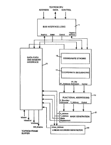
Figure 1 is an overview of a graphics subsystem in which the present
2 0 invention may be utilized. Bus interface logic 11 is connected through
address, data and control buses to a central processing unit (not shown).
The functional components of the graphics subsystem are data path and
mernosy interface 13, coordinate staging section 15, coordinate sequencing
section 17, functional address~ng block 19, mask generation block 21 and
2 5 linear address generator 23.
Data path and memory interface 13 update a frame buffer (not
shown) which is a mernory which stores graphical in~ormation to be
-8 -
132~sl.~
displayed on a video display such as a C~T. That is, data which is loaded
into the frame buffer is accessed by video circuitry which converts the
data to appropriate electrical signals which, in tum, turn individual pixels
of the video display on and off. The data from bus interface logic is
5 modified by mask generation block 21 and linear address generator 23
based upon processing performed by coordinate staging section 15,
coordinate sequencing section 17 and functional addressing stage 19.
Functional addressing stage 19 also accomplishes a portion of the clipping
necessary to fit particular graphic objects to the clip window in which they
10 are to be displayed, and then transfers the signals to mask generation
stage 21 which arranges the information into sixteen pixel portions tha~
traverse from the beginning to the end of the visible object for each scan
line and are used for address~ng the data-;path and memory interface stage
13.
The mask generation signals are also furnished to linear address
generator 23 whi~h translates the addresses provided by the mask
generation stage 21 into signals for line~rly addressing the frame buffer
for transfer to the output display. One embodiment of dala path and
memory interface block 13 may be found in copending application Serial
Ho. 600,289 filed May 19, 1989, Ho. 601,067 filed May 24, 1989
and No~ S00,158 filed May 19, 1989. An embodiment of coordina~e
sequencing logic 17 is disclosed in co-pending application Serial
No~ 611,654 filed September 1S, 1989. An embodi~ent of functional
addressing block 19 is disclosed in co-pending Serial Nos. 611,651
and 611,652 both filed Septembe~ 15, 1989. An embodiment of linear
address generator 2~ is disclosed in co-pending application Serial
No. 609,703 filed August 29, 1989. The present
invention is directed to circuitry in coordinate staging block
g
~,
~. ~
~32Q~8~
15 which performs certain operations based upon its inputs, the specifics
of ~vhich will be described belc~w with re~erence to figures 2-14 generating
infonnation in the nature of control signals to enable a graphics subsystem
to perform arbitrary quadrilateral rendering with clipping and block image
5 transfers (BLITs) with clipping. Thus, the present invention is directed to
specific circuitry within coordinate staging section 15.
Implementation of the various timing and control signals needed for
the proper operation of the foregoing functional blocks comprising a video
display subsystem are well known to persons skilled in the art and,
therefore, will not be described herein except as necessary for a proper
understandillg of the invention.
Referring now to figure 2~ a block overview diagram of coordinate
staging section 15 is shown. Coordinate stag~ng section lS comprises adder
15 31, loading control state machine 33, multiplexer 35, XY coordinate
registers 37, clip coordinate registers 39, raster offset registers 41, index
logic 43, test w~ndow control logic 45, comparison logic and result storage
47, comparison control state machine 49, and status genera~ion logic S 1.
Be~ore setting forth the specifics of the present invention, a brief
description of the manner in which objects are represented follows to aid
~he understanding of the manner in which the present invention is
implemented.
XY pairs of vertices represent video display coordinates. For a
~5 typical display, X ranges between 0-llS1 and Y ranges between 0-899.
Each X coordinate and each Y coordinate is stored in a separate 32 bit
register or a pair of 16 bit registers. Although 16 bits are more than
- 1 0 -
132~79~
adequate to store the largest screen coordinate (i.e., up to 65535 or -32768
to ~32767), 32 bits of information are stored because it is the data type
most prevalent in graphics software and provides a large enough range to
handle most real life objects ~hich may span areas much larger than the
5 video display.
Quadrilateral o~jects are represented as combinations of four pairs of
vertices (Xo,Yo), (Xl,Yl), (X2,Y2), and (X3,Y3). If an object is a point, then
all four pairs of ver~ices are the same or three points repeated. If an
obje'ct is a line, then two of the four (or three of the four) pairs of verticesare replicated. If an object is a triangle, then one pair of vertices out of thefour paLrs is replicated. If an object is a quadrilateral then all four pairs
are distinct. Objects (i.e., po~nt, l~ne, triangle or quadrilateral) are most
efficiently defined using the minimum number of unique vertices
necessary to completely define the object, i.e., for a point - 1, for a line - 2,
for a triangle - 3, for a quadrilateral - 4 and for a rectangle - 2 (opposite
corners3.
If a block image transfer (BLIT) operation is to be performed, then
the ~our X/Y registers have the following inte{pretation and are loaded
20 ~ccordingly:
X0 - X coordinate for upper left corner of the source block.
Y0 - Y coordinate for upper left corner of the source block.
Xl - X coordinate for lower right corner of the source block.
Y1 - Y coordinate for lower right corner of the source block.
~32~
X2 - X coordinate for upper left corner of the destina~ion block.
Y2 ^ Y coordinate for upper left corner of ~he destination block.
X3 - X coordinate for lower right corner of the destination biock.
Y3 - Y coordinate for lower right corner of the des~ination block.
Images to be displayed on a display such as a CRT are folmed as
discrete pixels which are stored in a random access memory (RAM) known
as a frame buffer in one or more planes (or bits), the number of planes
0 typically being eight for a color system. Data stored in the frame buffer is
addressed by a pair of coordinates, X and Y, where an X,Y pair identifies a
pariicular pixel in all planes, X being the row and Y being the column. A
pL~cel is defined by a single bit from each plane. Thus, if eight planes are
utilized, each displayed pixel is defined by eight bits in the frame buffer.
5 In this manner, one bit of a pLxel can be used to specify whether it is on or
off, with the remaining seven bits specifying the color of the pixel, or all
eight pixels can be used to specify the color, with one of the colors being
the same as the background color of the d;splay to turn the pixel off.
2 0 The present invention lies mainly in its irnplementation of index logic43, comparison logic and result storage 47 and comparison control state
machine 419 which orchestrates the acquisition of inter coordinate and clip
window coordinate comparison information. In this connection, Wit31
respect to the other functional blocks shown in Figure 2, their operation
and implementation will be described only in such detail as is necessary
for a proper understanding of the present inYention.
Adder 31 and MUX 35
-12-
~32~
Adder 31 is a 16 or 32-bit 2's complement binary adder having ~wo
inputs, namely DataIn from lbus interface logic 11 which represents
incoming data from the CPU and an input from MUX 35 which is a
multiplexer which selects one of a set of inputs from raster offset registers
47, X/Y coordinate registers 37, or clip coordinate registers 39. The input
from MUX 35 is selected by signals generated by loading control state
machine 33 as described below.
The details of adder 31 and multiplexor 35 will now lbe described
with reference to Figure 3. In Figure 3, adder 31 is shown as a 16 bit
adder. In this connection, although a 32 bit adder could ~e used since
Dataln in the preferred embodiment is 32 bits, in order to save space on
the integrated circuit in which the invention is imp1emented and since
timing requirements of the pipeline utilized by the present inventivn are
satisfied by a two step add, the following description will be directed to a
16 bit adder. The differences for utilizing a 32 bit adder will be apparent
to those skilled in the art and, there~ore, will not be described.
Multiplexor 35 is actually a pair o multiplexors 35a and 35b and a
third multiplexor 36 which is used to input the high order and low order
16 bits from Dataln. Multiple~cor 35a and 35b receive the high order and
low order 16 bits respectively from seven 32 bit inpu~s as f~llows: one 16
bit input (sign extended to 32-bits) ~rom raster offset registers 41, four 32
bit inputs from X/Y coordinate registers 37 and two 16 bi~ inputs (sign
extended to 32-bits) from clip coordinate registers 39. The outputs from
2 5 multiplexors 35a and 35b are combined to fonn the signal DataOut (for
providing read access to these register values to the CPU) and are also
input to a th~rd multiplexor 40 which passes the output from multiplexor
- 1 3 -
~32~
35a whenever the high order bits ~rom Xo-X3 or Yo-Y3 are belng accessed;
otherwise multiplexor 40 selects the output from multiplexor 3Sb. The
output from multiplexor 40 is one input to logic gate 42 which either
passes the 16 bit output from multiplexor 40 or passes 16 bits of ~eros. ln
5 this connection, zeros are forced by logic gate 4~ whenever the bits of
DataIn are passed by multiplexor 36 for directly loading (absolute loading)
into a register within raster offset registers 47, X/Y coordinate registers
37, or clip coordinate registers 39. Also shown in Figure 3 are logic circuits
44 and 46 which perform the ~ollowing function. When a low order 16-bit
0 add is taking place, AND gate 44 has its output ~orced to a low providing a
carry-In of a "O" to the adder 31. The carry owt of this add is saved in flip
flop 46. The output of flip flop 46 is gated by AND gate 44 to the carry in
of adder 31 during the addition of the up~per 16-lbits. This combination
provides a 2 cycle 32-bit add equivalent to a single cycle 32 bit add.
The operation of adder 31, raster offset registers 41, X/Y coordinate
registers 37, clip coordina~e registers 39, test window control 45 and
comparison logic and result storage 47 are coordinated by loading control
state machine 33 and comparison logic state machine 49 which causes the
2 aforesaid functional blocks to operate so that the data is flowing in a
pipeline. Thus, although not all sontrol lines frorm loading çontrol state
machine 33 and ~omparison logic state machine 49 are shown, the details
will be readily apparent to those skilled in the art from the description of
loading control state machine 33 and comparison logic state machine 49
below .
. 25
X~Y Coordinate Re~isters 37
- 14-
132~
X/Y coordinate registers 37 is, referrirlg to Figure 4, a set of 16-bit
registers which store the (Xo,Yo~-(X3,Y3) vertices of an object to be drawn.
One 16-bit regis~er is used to store the upper 16 bits of e~ch X coordinate
and another 16-bit register is used to the store the lower 16 bits of each X
5 coordinate. Similarly, another 16-bit register holds the upper 16 bits of
each Y coordinate and another 1 6-bit register holds the lower 16 bits of
each Y coordinate. These registers are shown in Figure 4 as XOL
representing the lower 16 bits of the Xo coordinate and XOU representing
upper 16 bits of the Xo coordinate. Registers XlL-X3L and XlU-X3U
lo represent the lower and upper 16 bits of the Xl-X3 coordinates
respestfully. Similarly registers YOL-Y3L and YOU-Y3U s~ore the lower
and upper 16 bits of the Y~-Y3 coordinates of the object. References to
XO,YO etc. mean the 32 bit value stored in the corresponding register pair,
i.e., XOU,XOL and YOU,YOL.
Each pair of registers, (XOL,YOI,)-(X3L,Y3L) are coupled to a
multiplexer pair which are used to select either the corresponding X or Y
register. For example, registers XOL and YOL are coupled to multiplexers
61a and 6tb. Loading control state rnachine 33 generates a signal which
directs multiplexer 61a to select the input from register XûL or YOL
depending upon the whether the X coordinates are to be operated upon or
the Y coordinates are to be operated upon. Each of multiplexers 62a and
6~b - 64a and 64b operate in the same manner respectively for data from
register pairs (XlL,YlL)-(X3L9Y3L). The outputs ~rom multiplexers 61a-
64a go to multiplexer 35b, while the outputs from multiplexers 61b-64b
go to comparison logic and result storage 47.
-15-
1 3 2 ~
Blocks 67, 69, 71, and 73 labeled All O's All l's are each logic
circuitry which chc,cks the upper 18-bits of i~s correspondin~ X,Y
coordinate pair for all zeros or all ones. Sixteen of the bits come from the
registers (XOU,YOU)-(X3U,Y3U) with the seventeenth and eighteenth bits
coming from the high order two bits of the corresponding register in the
gtouping (XOL,YOL-X3L,Y3L). The seventeenth and eighteenth bit input is
not shown in Figure 4 to avoid unnecessarily cluttering the figure. The
register pairs (XOU,YOU~-(X311J,Y3U) are input into multiplexers 75-78
respectively which select either the X coordinate or Y coordinate in the
0 same manner as multiplexer pairs 61a,61b-64a,64b. The outputs from
multiplexers 75-78 go to multiplexer 35a. One of the 4-bits output from
each of logic blocks 67-73 are each a "1" if the upper 18-bits of its
corresponding register are all ~eros or all ones, otherwise each of the 4-bits
is zero. The four 4-bit outputs from blocks 67-73 are input into status
generation logic 51.
C~ e~isters 39
Clip coordinate registers, as shown in Figure 5 comprises four
registers, XClipMin, XClipMax, YClipMin, YClipMax and multiplexors 81a,
81b, 83a and 83b. The values XClipMin, XClipMax, YClipMin, YClipMax,
which are stored in the aforesaid registers with the same name,
~espectively define the left, right, top and bottom of the currently active
window. These values are generated by the CPU and are input to adder 31
whic,h adds O to these values for loading the registers XClipMin, XClipMax,
YClipMin, and YClipMax as described above. Multiplexors 81a and 83a on
the one hand, and multiplexors 81b and 83b on the other, select XClipMin
and XClipMax or YClipM~n anc3 YClipMax, depending on control signals
- 1 6 -
~ 3 2 ~
generated by loading control state machine 33 and comparison control
state machine 49 respectively. The values from multiplexors 81a and 83a
are sent to multiplexor 35, while the values from multiplexors 81b and
B3b are sent to comparison logic and result storage 47 and test window
5 control 45.
Raster Offset Registers ~1
Raster offset registers 41, as shown in Figure 6 comprises two
registers, XRasOff, YRasOff, and multiplexor 53. The values XRasOff and
0 YRasOff, which are stored in the aforesaid registers with the same name,
respectively define the X and Y offset to be added (when desired) to
DataIn before storage into each of the four sets of X,Y coordinates in X/Y
coordinate registers 37. These values are generated by the CPU for storage
in XRasOf~ and YRasOff. Multiplexor 53 selects XRasOff or YRasOff
5 depending on control signals generated by loading control state machine
33. The value selected by multiplexor 53 is sent to multiple:xor 35.
Test Window Control 45
Test window control 45 will now be described with reference to
20 Figure 7. The CPU generates the v~lues testXVal and testYVal which offset
a predetermined distance, i.e. number of pixels, above and below (for
testYVal) and to the ~ight and left (for testXVal) of the currently active
clipping window. That is, for a given window on a display, there is a ~X
and ~Y which define a test window surrounding the real clip window. The
2 5 purpose of this test window is to eliminate, whenever it is beneficial to do so, the need for the hardware to calculate the location of objects or
portions of the objects which are outside the clipping window. Details
-17-
~L32~5~
concerning the use of the test window are described in copending
application Serial No.
The 4-bit values testXVal and testYVal are stored in the 4-bit
registers ~estX and testY respectively. Multiplexer 91 selects one of the
registers tcstX or testY depending upon whether the X coordinates or the Y
coordinates are being operated upon as determined by the signal MUX
Enable generated by the loading control state machine 33. The output of
multiplexer 9 l is input into decrementor 93 and incremerltor 95 .
Dec~ementor 93 has as a second input the value XClipMin or YClipMin and
incrementor 95 has as a second input the value XClipMax or YClipMax,
again depending upon whether X or Y coordinates are being operated upon
as deterrnined by the signal MUX Enable generated by the loading control
state machine 33. The outputs generated by decrementor 93 and
incrementor 95 will be referred to as XTestMLn, YTestMin and XTestMax,
YTestMax respectively. Decrementor 91 creates the values XTestMin and
YTestMin by subtracting from XClipMin and YClipMin a value equal to 2
raised to (testX-1) and (testY-1) power respectively. Similarly,
incrementor 93 creates the Yalues XTestMax and YTestMax by adding to
XClipMax and YClipMax a value equal to 2 raised ~o the (testX-l) and
(testY-1) power respectively. (i.e., 2(testX-1) or 2(testY-l)
Loadin~ Control State Machine 33 and Index Lo ic 43
Loading control state machine 33 generates the control signals, ~UX
25 Enable, lndex and Register Fnable. MUX Enable is a set of control signals,
one of which causes the various multiplexors in raster offset registers 41,
X/Y coordinate registers 37 and clip coordinate registers 39 to select their
-18-
~ 3 ~
respective X inputs or Y inputs; a second o which causes multiplexor 35 to
select one of the inputs from raster offset registers 41, X/Y coordinate
registers 37 or clip coordinate registers 39. lndex is a single control signal
which causes an index re~ister in index logic 43 to increment by 1 between
5 for each of the values 0, 1 and 2, and if the value is 3, to reset to 0 (modulo
4). Register Enable is a set of control signals, one for each of the registers
in raster offset registers 41, X/Y coordinate registers 37 and clip
coordinate registers 39, enabling each such register to load the 16 bit value
on the line from adder 31.
The operation of load con~rol state machine 33 and index logic 43
will now be described by way of an example from which ehe
implementation details should be apparent. As noted above, images to be
drawn are defined as being made of one or more objects having four pairs
of vertices, (Xo,Yo) - (X3,Y3). Objects may be points, lines, triangles,
rectangles or quadrilaterals. For points, the four pairs of vertices are
identical For l~nes, there are only two pairs of unique vertices. Four sided
quadrilate~rals have four unique vertices. A rectangle represents a special
case of quadrilateral wherein there are only two unique X coordinates and
two uniqus Y cvordinates (rectangles can be de~ned by a pair of vertices
defining diagonally opposite cvrners). For triangles, there are only three
pairs of unique vertices.
The index value specifies which registers to enable based upon the
type of object being defined. For proper operation, Y values precede X
25 values. Except for rectangles, the index register is incremented after the X
values have been loaded in the appropriate registers. For rectangles, the
index register is incremented after both X and Y values. ln this connection,
- 1 g -
~ 3 2 ~
the following table sets forth ~r each type of object, the X registers which
are enabled for each index register value. Although not shown, the
enabled Y registers would correspond to the enabled X registers.
TABLE I
Index Value At T~me Of Load
Object Type 0 l 2 3
point X0,Xl,X2,X3Xl,X2,X3,X0X2,X3,X0,Xl X3,X0,Xl,X2
line X0,Xl,X2Xl,X2,X3 X2,X3,X0 X3,X0,Xl
quadrilateral X0 Xl X2 X3
rectangle X0,Xl Xl,X2 X2,X3 X3,X0
'- 10
- An important point that can be seen in Table I is that the coordinate
pointed to by the index register is always written. The type o write
(point, line, triangle, etc.) indicates how many subsequent registers
15 (modulo 4) will also be written. For example, if the index is 2, at the time
a line X write is received, then three registers will be written, namely X29
(X2 + l) modulo 4 and (X2 + 2) modulo 4 or X2, X3 and X0. A quadrilateral
write to Y would only affect Y2.
Examples 1-3 below will expla~n the role of the index register when
20 defining an object. Each line of the example indicates the intended write
operation, the index register value utilized by the loading control state
machine to govern the luading of the coordinate registers, the values
stored in the coordinate registers after the write, and the index value after
the write cycle concludes. The mnemonics for the write commands are
25 PntX or PntY to indicate a point write, LineX or LineY for a line write, TriXand TriY for a triangle write, QuadX and QuadY for a quadrilateral write,
-20-
1~2~
and RectX and ReceY ~or a rectangle write operation. The actual write
operation identified by each write command is actually a multi-clock cycle
operation as will be described later. lFor these ex~nples though, the
execution time of the command is of no relevance.
As a means of clarifying the in~erpretation of these examples, the
first one will be described. From this description the interpretation of
Examples 2 and 3 should be readily apparent.
At the time the PntY(6) command is received, all coordinate registers
0 contain the value "0" and the index is equal to "1". The PntY(6) cornmand
says that a pomt of value 6 should be loaded into the Y coordinate
registers~ Since the index is a 1, Table I indicates that the incoming value
(6~ should be stored into Yl, Y~, Y3 and Y0. The next command received,
PntX(3), then says to load the point 3 into Xl, X2, X3 and X0. As is the case
15 after all indexed X coordinate writes, the index is incremented (modulo 4)
at the end of the write cycle. The next wrilte command is a L~neY(9). The
index for this load is 2 and Table I indicates the loading of 9 into Y2, Y3
and Y0. The final write command for this example is LineX(7). Table 1
indicates the loading of 7 into X2, X3 and X0 after which the index register
20 is again incremented. The final state of the coordinate registers identify
two unique vertices (3 ve~tices at (7, 9) and one at ~3, 6)~. Geometrically,
this is a line with endpoints at (7, 9) and ~3, 6) as was intended.
1~2~$~
E~ample 1 Specifying a line (3, 6) (7, 9)
Index Index
Before After
Command_. XO Xl X2 X3 YO Y1 Y2 Y3 Write Write
- O ~ O O O O O O ûl 01
write PntY(6) O O O 0 6 6 6 6 01 01
5write PntX(3) 3 3 3 3 6 6 6 6 01 0 2
write LineY(9) 3 3 3 3 9 6 9 9 0 2 0 2
write LineX(7) 7 3 7 7 9 6 9 9 0 2 0 3
Example 2 Speci~ying a triangie (1,5~ (993~ (4,6)
` Index Index
Before After
Command XO X1 X2 X3 YO Yl Y2 Y3 Write Write
- 7 3 7 7 9 6 9 903 03
write TriY(5) 7 3 7 7 5 6 9 50 3 0 3
write TriX(1) 1 3 7 1 5 6 9 50 3 0 0
write TriY(3) 1 3 7 1 3 3 9 50 0 0 0
write TriX(93 9 9 7 1 3 3 9 50 0 01
write TriY(6) 9 9 7 1 3 6 6 501 01
writ~ TriX(4) 9 4 4 1 3 6 6 5O 1 0 2
Example 3 Specifying a Reetangle (0,7) (B,7~ (8,1) (0,1)
Index Index
Before After
Command X() X1 X2 X3 YO Y1 Y2 Y3 Write Wr~te
- 9 4 4 1 3 6 6 50~ 0
write RectY(1) 9 4 4 1 3 6 1 1 0 2 0 3
write ~ectX(O) O 4 4 0 3 6 1 1 0 3 0 0
write RectY(7) 0 4 4 0 7 7 1 1 0 0 0 1
write RectX(8) 0 8 8 0 7 7 1 1 01 0 2
~32~
Although in example 1, the index register is arbitrarily 1 when the
f~rst coordinate is received, the index register in index logic 43 may be
initiali~ed based up~n a value placed on Dataln if instructed by the CPU.
(It is worth noting, however, that proper operation of this invention is
5 totally independent of the initial value of the index register when a loading
sequence is ~nitiated.). It is also assumed in this example that XRasOff and
YRasOff contain the value 0 so as not to obscure the operation of this
clrcuitry.
' Loading control s~ate machine 33 in conjunction with comparison
logic state machine 49 controls a pipelining scheme which in addition to
loading the various registers described above, also controls the selection of
registers and corresponding multiplexors necessa:ry for the proper
operation of comparison logic and result storage 47 and status generation
logic Sl. Addi~ionally, when it is desired to not utilize ~he raster offset
capability of the present invention, it is necessary to force the addition of
O's to the incoming d~ta for storage into the X and Y coordinate registers
prior to perfonning the comparisons performed by comparison logic and
result storage 47.
1D this connection, the MUX Enable, and Register Enable control
signals generated by loading control state machine 33 and comparison logic
state machine 49 may be ascertained from the timing sequellce table set
forth in Figure 9 and the following list showing the order of processing
performed by coordinate staging section 15 for each entered Y coordinate.
1. Receive Y coordina~e on DataIn
-~3 -
~ 3 2 ~
2. Add the low order 16 bits of the received Y coordinate to.
a) YRasOff (lower 16-bits)
or b) the low order 16 bits of YOL-Y3L pointed to by (index-l)
or c) O's
5 3. Add the high order 16 bits of the received Y coordinate to:
a) YRasOff (sign extended upper 16-bits)
o~ b) the high order 1~ bits of YOH-Y3H pointed to by (index-1)
or c) O's
and compare the result of step 2 to the other Y coordinates
4. C:ompare the result of s~ep 2 to YClipMin, YTestMin, YClipMax, and
0 YTestMax and examine the upper 18 bits of the result of steps 2
and 3 for all l's and all O's.
In steps ~ and 3 above, the choices a), b) or c) are made as follows.
For non-relative writes to an indexed register (PNT, LINE, TRI, QUAD, RECT)
choice a) is selected. For a relative wr~te to an indexed register (RELPNT,
RELL~E, RELTRI, RELQUAD, REL~CT) choice b) is selected. All other
writes select choice c). The loading of an X coordinate follows the same
flow.
With the foregoing restrictions and definitions in mind, and assuming
that the index register value in index logic 43 is 'Ol' and registers (XO,YO) -
~X3,Y3) as described above with reference to Figure 4 are all O, the
~ollowing sequence of events takes place to load the registers so as ~o
define a line having endpoints whose X,Y coordinates are (3,6) (7,9) as ~n
Example 1.
At clock cycle O, the command write Pn~Y(6) places the value 6 on
Dataln, and causes the register address input to loading control state
- 2 4 -
132~5?,l~
machine 33 to contain a value indicating that the incoming da~a is a Y
point. At clock cycle 1 (and referr~ng to Figure 3), multiplexor 36 is
instructed to select the low order 16 bits on DataIn and multiplexors 35
(i.e., multiplexors 35a and 35b) and 40 and logic gate 42 are instructed to
5 pass the lower 16 bits of YRasO~f. Thus> during clock cycle 1, adder 31
adds the outputs from multiplexor 36 and logic gate 42 and places the
result at its ou~put. At the end of clock cycle 1, registers YOL-Y3L are
enabled and loaded with the value from adder 31, i.e., 6 reprçsenting the
low order bits of the value 6 that was on DataIn. At clock cycle 2,
0 multiplexor 36 is instructed to select the high order 16 bits on DataIn and
multiplexors 35 and 40 and logic gate 42 are instructed to pass the sign
extended upper 16 bits of YRas(~ff. Thus, dluring clock cycle 2, adder 31
adds the outputs from multiplexor 36 and logic gate 42 and places the
result at its outpu~. At the end of clock cycle ~, registers YOH-Y3H are
15 enabled and loaded with the value ~rom the olltpUt of adder 31. At cycle
3, the cor:nmand write PntX(3) places the value 3 on DataIn, and causes the
register adldress input to loading control state machine 33 to contain a
value Lndicating that ehe incoming data is an X point. Also at clock cycle 3,
multiplexor 36 is instructed to select the low order 16 bits on DataIn and
2 0 multiplexors 35 and 40 and logic gate 42 are instructed to pass the lower
16 bits of XRasOf~. During clock cycle 3, adder 31 adds the outputs from
multiplexor 3S and logic gate 42 and places the result at its output. At the
end o clock cycle 3, registers XOL-X3L are enabled and loaded with the
value from adder 31, i.e., 3 representing the low order bits of the value 3
25 that was on DataIn. At clock cycle 4, multiplexor 36 is instructed to select
the high order 16 bits on DataIn and multiplexors 3S and 40 and logic gate
42 are instructed to pass the sign extended upper 16 bits of XRasOff. At
~5
132~
clock cycle 4, adder 31 adds the outputs from multiplexor 36 and logic gate
42 and places the result at its output. During clock cycle 4, registers XOH-
X3H are enabled and loaded with the value from the ou~put of adder 31,
and the index register is incremented. A~ clock cycle S, the command
write LineY(9) places the value 9 on Dataln, and causes the register
address input to loading control state machine 33 to contain a value
indicating that the incorning data is a Y line. At clock cycle S, multiplexor
36 is instmcted to select the low order 16 bits on DataIn and multiplexors
35 and 40 and logic gate 42 are instructed to pass ~he lower 16 bits of
0 YRasOff. During clock cycle 5, adder 31 adds the outputs from multiplexor
36 and logic gate 42 and places the result at its output. At the end of clock
cycle S, ~egisters Y2L, Y3L and YOL are enabled and loaded with the value
from adder 31, i.e., 9 representing the low order bits of the value 9 that
was on DataIn. At clock cycle 6, multiplexor 36 is instructed to select the
high order 16 bits on DataIn and multiplexors 35 and 40 and logic gate 42
are inst[ucted to pass the sign extended upper 16 bits of YE~asOff. At clock
cycle 6, adder 31 adds the outputs from multiplexor 36 and logic gate 42
and places the result a~ its output. During c:lock cycle 6, registers Y2H, Y3H
and YOH are enabled and loaded with the value from the output of adder
31. At clock cycle 7, the command write LineX(7) places the value 7 s)n
DataIn, and causes the register address input to loading control state
machine 33 to contain a value indicating that the incoming data is an X
line. In a like manner registers X2L, X3L and XOL are eventually enabled
to load the value 7 after which the index register is incremented from 2 to
2 5 3 as shown above. Loading X/Y coordinate registers for other objects
follows the same pipeline scheme described above. Examples for triangles
- 2 6 -
~32~8~
and rectangles are given in examples 2 and 3 above~ In a similar manner,
quadrilateral objects are also loaded~
Raster offset registers 41 and clip coordinate registers 39 are loaded
in a similar manner as XJY coordinate registers 37 as described above,
however, logic gate 42 is instructed to force O's for each add cycle~ (i.e~,
absolute loading)
The present invention, by use of the index register in index logic 43
also. performs relative addressing which provides an efficient mechanism
10 ~or displaying duplicates of objects. Relative addressing is best described
by way of an e~ample as follows. The three vertices of a triangle may be
defined as (Xo,Yo), (Xl,Yl) and (X2,Y2~. To duplicate this object 50 times
at differen~ locations on the display, it would be necessary to store 150
pairs of X,Y coordinates. Using relative addressing, one vertex is defined as
1S the ongin ~Xo,Yo), and the second and th~rd vertices are de~ined as offsets
from the previous vertex, i.e., ~Xol,~Yol and ~X23,~Y23. To duplicate the
object 50 times, all that needs to be stored are the two offset pairs and a
new Xo,Yo for each duplicate (i.e. fifty object origins plus ~wo offset pairs
~otal~.
This can be accomplished in the present invention by first storing the
origin coordinate pair vertex in one of the register pairs within X/Y
coordinate registers 37 using an indexed loading style ~i.e., PntY, PntX).
The ~wo offset vertices are subsequently stored relative to the vertex
25 pointed to by the current value of the index register. This is accomplished
by selecting the vertex pointed to by (index -1) to be added to DataIn
prior to register loading. The vertex referenced by (index -1 ) is
- 2 7 -
132~
guaranteed to have been l~aded on the previous inde~ed write irrespective
of the type of write (PNT, LINE, etc.) and is, therefore, the vertex from
which th~ relative offset applies.
Comparison lo~ic and result storage logic 47
Comparison logic and result storage logic 47 will now be described
with reference to Figures 7 and 8. Comp~ison logic and result storage
logic 47 comprises multiplexors 101~ 103, lOS, 107 and 109 (see Figure 7~,
and, comparators 121-124, multiplexors 131-146 and registers Rl-R44
o (see Figure 8).
Registers Rl-R4~ store the results of the operation of comparators
121-124 as shown in Table II:
TABLE II
Rl XO:XClipMin R23 YO:YClipMin
R2 XO:XTestMin R24 YO:YTestMin
R3 XO:XClipMa~ R25 YO:YClipMax
R4 XO:XTestMax R26 YO:YTestMax
R5 Xl :Xs~lipMin R27 Yl :YClipMin
R6 Xl:Xl~estMm R28 Yl:YTestMin
R7 Xl:XClipMax R29 Yl:YClipMa~
R~ X 1 ;XTestMax R30 Y 1 :YTestMax
R9 X2:XClipMin R31 Y2:YClipMin
R10 X2:XTestMin R32 Y2:YTestMin
Rll X2:XClipMax R33 Y2:YClipM~
R12 X2:XTestMa~ R34 Y2:YTestMax
R13 X3:XClipMin R35 Y3:YClipMin
R14 X3:XTestMin R36 Y3:YTestM~n
RlS X3:XClipMa~ R37 Y3:YClipMax
R16 X3:XTestMax R38 Y3:YTestMax
R17 XO:Xl R39 YO:Yl
R18 XO:X2 R40 YO:Y2
Rl9 XO:X3 R41 YO:Y3
R20 X 1 :X2 R42 Y 1 :Y2
-28-
~32~$~
R21 Xl:X3 R43 Yl:Y3
R22 X2:X3 R44 Y2:Y3
In Table Il, excepting for the comparisons involving XClipMin/Ma~,
YClipMin/Max, XTestMin/Max, and YTestMinJMax which store a one bit
5 result, the indicated register stores a two bit result of a comparison
between the two indicated values. If the value on the left o the colon is
~reater than the value to the right of the colon, the binary value stored in
the correspond~g register is '10'; if the value on the left of the colon is lessthan the value to the right of the colon, the binary value stored in the
0 corresponding register is '01'; if the two values are equal, the binary value
stored in the corresponding register is '00'. For XClipMin, YClipMin,
XTes~Min, and YTestMin, if the coordinate value compared is less, a '1' is
stored, otherwise, a 'O' is stored. For XClipMax and YClipMax, XTestMax,
YTestMax if the value compared is greater, a '1' is stored, otherwise, a 'O' is
1 5 stored.
The inputs to multiplexors 101, 103, 105, 107 and 109 are from X/Y
coordinate registers 37, namely XOL,YOL - X3L,Y3L, clip coordinate
registers 39, namely XClipMin,YClipMin and XClipMax,YClipMax and test
20 w~ndow control 45, namely XTestMin, YTestMin, XTestMax and YTestMax.
Of course, at any one ~ime, the inputs to multiplexors 101, 103, 105, 107
and 109 are either X values or Y values as described above, based upon a
MUX Enable signal generated by comparison control sta~e machine 49.
Cornparator 121 compares multiplexor 101 output and multiplexor
~5 109 output. Similarly, comparators 122-124 compare multiplexor 103,
105 and 107 outputs on the one hand and mul~iplexor 109 output on the
other. l`he outputs from comparators 121-124 are input to multiplexors
- 2 9 -
~L '3 2 ~
131-146 which direct the appropriate data to registers Rl-R44 to be
loaded as follows.
The output from comparator 121 is connected to multiplexors 131-
135, 139 and 143 which are used to load registers Rl, R2, R3, R4, R5, R9,
R13, R17, R18, and R19, for X values and registers R23, R24, R25, R26, R27,
R31, R35, lR39, R40, and R41 for Y values as shown in Figure 8 and Table Il
below. In Table III, A, B, C,and D refer to comparators 121, 122, 123 and
124 respectively.
0The output from comparator 122 is cs:~nnected to multiplexors 132,
135, 136, 137, 138, 140, and 144 which are used to load registers R2, RS,
R6, R7, R8, R10, R14, R17, R20, and R21 for X values and registers R24,
R27, R28, R29, R30, R32, R36, R39, R42 and R43 ~r Y values as shown in
Figure 8 and Table IIl.
The output from comparator 123 is connected ~o multiplexors 133,
137, 139, 140, 142, and 145 which are used to load regis~ers R3, R7, R9,
R10, E;t12, R15, R1~, R20 and R22 for X values and registers R25, R29, R31,
R32,, E~34, R37, R40, R42, and R44 for Y values as shown in Figure 8 and
20 Table III.
The output from comparator 124 is connected to multiplexors 134,
138, 142, 143, 144, 145 and 146 which are used to load registers R4, R8,
R12, R13, R14, R15, R16, R19, R21, and R22 for X values and registers R26,
R30, R34, R35, R36, R37, R38, lR41, R43 and R44 ~or Y values as shown in
2 5 Figllre 8 and Table lII.
- 3 0 -
~ 32~5~
The comparisons done and stored are those required by coordinate
sequencing block 17 and functional address~ng block 19 in order to
properly execute supported operations (DRAW, also known as quadrilateral
rendering, or BLIT) and perfo~n proper clipping.
Comparison Con~rol State Machine 4~
Comparison control sta~e machine 49 is logic which enables the
va~ious comparators, multiplexors and registers in comparison logic and
result storage 47. A trath table for absolute loading o the coordinate and
0 clipping registers by the companson control state machine 49 is shown in
Table III or clock cycles O and 1, with comparators 121-124 referenced A,
B, C and D respectively. Table III sets forth the output of each comparator
121-124 for each of the inputs XOL-X3L, XClipMin, XClipMax, XTestMin and
XTestMax. In this connection, althoogh Figure ~ shows that ~he outputs of
5 multiplexors 101, 103, lOS and 107 are input into one side of comparators
121-124, with the output of comparator 109 being input into the other
side. For consistency, it is necessary to store ~he comparisons of XOL to
XlL, XlL to X2L a~nd X2L to X3L etc., rather than the other way around
(e.g., XlL to XOL). For this reason, when the column labeled reverse is
20 "yes," the outputs from comparators 121-124 are reversed. This is
handled by the right input of multiplexors 131-146. The output from the
indicated comparators 121-124 are directly inpu~ to the left side of the
indicated multiplexor 131-146. The right multiplexor input receive the 2
bit output from the indicated comparator in reverse bit order. Thus, the
2 5 column labeled reverse becomes the truth table for the MUX select line
lines for multiplexors 131-1~6 ~or absolute courdinate loads.
-3 1 -
~32~
TABLli ~I
COMPARATOR COMPARISON REVERSE CYaE
WRrrE TO XO
B XOL:XlL YE~ O
C XOL:~L 1~ 0
D XOL:X3L YE~ O
A XOL:XClipMin
B XOL:XTestMin Yl~
C XOL:XClipMa~ YES 1
D XOL:XTestMa~c YE~ 1
WRl'I~ TO Xl
A XlL:XOL NO O
C XlL:X2L YES O
D XlL:~L YE~ O
A XlL:XClipMin YES
B XlL:XTestMin Y~
C XlL:XClipMa~ YES
D X lL:~TestMax YE~ 1
WRlTE TQ X2
A X2L:XOL N~ O
B X2L:XlL NO O
D X2L:X3L YES O
A X2L:XClipMin Y~
B X2L:XTestMin Y~
C X2L:XClipMax YES
2 o D X2L:XTestMa~c YE~ 1
WR lrrE TO X3
A X3L:XOL N~ O
B X3L:XlL N~ O
C X3L:X2L N[~ O
A X3L:XClipMin Y~
B X3L-XTestMin YES
2 5 C X3L.XClipMax YE~ 1
D X3L:XTestMax YlE3
- 3 2 -
132~$l,~
COMPARATOR COMPARlSON REVERSE CY~E
WRlTl~ TO XClipMin
A XClipMin:XOL ND O
B XClipMin:XlL N~ . O
C XClipMin:X2L NO O
D XClipMin:X3L N~ O
A XTestMLn:XOL N~ 1
B XTestMin:XlL NO
C XTestMin:X2L NO
D XTestM~n:X3L NO
WRl~E TO XClipMax
A XClipMax:XOL N~ O
10' B XClipMa~:hlL ~ O
C XClip~ax:X2L N~ O
D XClipMax:X3L ~) O
A XTestMax:XOL N~ 1
B XTestMa~:XlL ~
C XTestMax:X2L N~ 1
D XTestMax:X3L N~ 1
The results of Table lII are repeated in a similar manner for YOL-
Y3L, l~ClipMin, YClipMax, YTestMin and YTestMax. Figure 9 shows the
relative tl!mings of the signals on DataIn, the register loading performed by
raster offset registers 41, X/Y coordinate registers 37, clip coordinate
registers 39 and comparison logic and result storage 47.
The comparison control state machine supports the indexed loading
scheme as previously discussed utilizing both the index register value
associated with a wIite cycle and Table IV. Since the register pointed to
by ~he index register value is always written irrespective of ~he type of
indexed write, the appropriate Mux Enables for MUXes lOl, 103, lOS and
l 07 are selected t~y the comparison control state machine assuming a
single register write to that coordinate. For example, if a rectangle write to
- 3 3 -
1320~$~
X with an index of 3 is receive~, the comparison logic will operate as if an
explicit wri~e to X3 was received and do comparisons X3L vs (XOL, XlL,
X2L, XClipMin, XClipMax, XTestM:Ln, XTestMax) as is requiled. The
di~ference be~ween an absolute loading of a register and an indexed (or
5 relative indexed) load is that in the indexed case, more than one coordinate
storage register in 47 may be enabled to receive the comparison results
and the multiplexor selects for rnultiplexors 131-146 are generated
according to Tabl~ IV instead of Table III.
ln the previous example of a rectangle X write with an index of 3,
comparison registers (refer to Table lI or Figure 8) R1-R3, R13-R16, R17-
R19, and R21-R22 are written. The following registers pairs will store the
same individual comparison results: (R17, R21), (R18, R22), (Rl, R13~, (R~,
R14), (R3, R15), and (R4, R16).
TABLE IV
COMPAR~TOR COMPARISONTYPE REVERSE IND~X
B XO:X1 PNT yes
C XO:X2 PNT y e s
D XO:X3 - PNT y e s
C Xl:X2 PNT yes
D Xl:X3 PNT yes
D X2:X3 PNT y e s
B XO:X1 LINE y e s O
C XO:X2 LINE y e s O
D XO:X3 L~E y e s O
C Xl:X2 I,INE yes O
D Xl :X3 LINE y e s O
2 5 D X2:X3 L~E y e s O
-34-
1~ 3 `~
COlMP~AIOR COMPA~SONTYPE REVERSE lNDEX
A XO:XI LINE nn
A X~:X2 LINE n o
A XO:X3 LIME n o
C: Xl:X2 LINE yes
D Xl:X3 LINE yes
D X2:X3 Ll~ y e s
A XO:Xl L~E y e s 2
C XO:X2 LIN y e s 2
XO:X3 LINE y e s 2
B Xl:X2 LlNE no 2
B Xl:X3 LINE no 2
C X2:X3 LINE y e s 2
A XO:Xl LINE y e s 3
C XO:X2 LINE y e s 3
D XO:X3 LINE y e s 3
C Xl:X2 L~ yes 3
D Xl:X3 LINE yes 3
C X2:X3 Ll~E n o 3
B XO:XlTRI/RECT yes
C XO:X2TRI/RECT y ~ s O
D XO:X3TRI/RECT y e s O
C Xl:X2TRI/RECT yes O
D Xl:X3TRI/RECT yes O
A XO:XlTRVRECT n o
A XO:X2TRIIR~ECT no
C Xl:X2TRI/RECT yes
D Xl:X3TRVRECT yes
D X2:X3TRl/RECT y e s
A XO:X2TRI/RECT n o 2
A XO:X3TRI, RECT n o 2
B Xl :X2I Rl/RECT n o 2
B Xl:X3TRUREcT no 2
2 s D X2:X3TRUREcT y e s 2
- 3 S -
~ 3 ~
COMPARATOR COMPARIS(:)NTYPE ~EVERSE ~DEX
B XO:Xl TRI/~ECT yes 3
C XO:X2 TRI/RECT y e s 3
D XO:X3 TRI/RECT y e s 3
B Xl:X3 T3~1/~CT no 3
C X2:X3 TRI/RECT n o 3
B XO:Xl QUAD y e s O
C XO:X2 ~JAD y e s O
D XO:X3 QUAD y e s O
A XO:Xl QUAr) n o
C Xl:X2 QUAD yes
D Xl:X3 QUAD yes
A XO:X2 QUAD n o 2
B Xl:X2 QUAD no 2
D ~:X3 QUAD yes 2
A XO:X3 QUAD n o 3
B Xl:X3 QUAD no 3
C X2:X3 (~UAD no 3
Status Generation Lo~ic 51
Status generation logic 5 l generates the control signals HW/SW,
Up/R-to-L and HID/VIS. HW/SW is a 2 bit signal indicating whether the
operation will be done by the hardware of the present invention or by
sof~ware. Up/R-to-L is a 2 bi~ signal indicating whether operatiorl should
be processed top to bottom, bot~om to top, right to left or left to right.
HID/VIS is a two bit signal indicating whether the object to be drawn is
hidden, i.e. behind the active clip window or visible. To generate these
signals, status generation logic Sl receives as inputs the registers Rl-R22
~or X coordinates registers R23-K44 for 1~ coordinates and the ~our 4 bit
signals indicating the upper 18 bits are all l's and all O's i~rom X/Y
-36-
132~
coordinate registers 37. The manner in which status generation logic
generates the foregoing control signals will be explained with re~erence to
Figures 10-14 which are truth tables for the logic performed by status
generation logic 51. The logie circuitry necessary to implement the truth
s tables of Figures 10-14 is well within the capabilities of persons skilled in
the relevant art.
Figure 10 is a truth table utilizing comparison results for the XO
coordina~e (XOL and XOH). Truth tables utili~ing comparison results for the
Xl-~3 and YO-Y3 coordinates by substituting those coordinates and using
YClipMin, YClipMax, YTestM~n and YTestMax in place of XClipMin,
XClipMa7c, XTestMin and XTestMax ~or the Y coordinates. The left side of
the table are the inputs and the right side are the outputs. In the table,
the symbol "-" is a don't care; O and !O means the bus bit values are all l's
or not all l's respectively (from XJY coordinate registers 37); and ~: and !Z
means the bus bit values are all O's or not all O's respectively (from X/Y
coordinate registers 37). "XO inside 214" means the 32 bit XO coordinate is
representable in 15 bits; "XO inside clip" means XO is on or inside the clip
window X boundaries; "XO inside test" means XO is on or inside the test
window X boundaries. The outputs "XO < XClipMin", "XO c XTestMin", "XO >
XClipMa~", and "XO > XTestMa~c" are fedback and used as inputs. To folm
the outputs, the inpu~s on a horizontal line are ANDed together and the
outputs in a column are ORed together. Thus, for example, re~erring to the
first two l~nes of Figure 10, if XO[31] (i.e., its sign bit) is O AND X0130:14]
~i.e., its high order bits 14-30) are all O's, OR XO[31] is 1 AND X0130:14] are
all l's, then XO is ~nside 214. Similarly, referring to the last line of Figure
- 3 7 -
~32~
lû, if XO ~ X'restMin is 0 (i.e. false) AND X0 > XTestMax is 0, then X0 is
inside the test window.
Figures 1 la and 1 lb are a truth table utilizing comparisons between
each of the four X vertices and each of the four Y vertices. As was the case
with Figure 10, the values on a horizontal input l~ne are ANDed together
with the result being a logical 1 (true) or 0 (false) and the indicated
outputs (e~cept ~or top, bottom, right and left) are formed by ORing its
corresponding column. The outputs top, bottom, right and left which are
shown as 0, 1, 2 or 3 are interpreted as follows. The value 0, 1, 2 or 3
specifies which coordinate of X0-X3 or Y0-Y3 is the largest (top~, smallest
(bottom), rightmost (right) and leftmost (lef~). The symbols <,>,E,L and G on
the input side indicate ~hat the specified comparison result is less than,
greater than, equal to, less than or equal to and greater than or equal to
respectively .
Although the meaning of the outputs is defined by the table, the
following sets forth in words what each indicated output means:
illegal - means that if a horizontal line is drawn through the objec~
defined by the four pairs of vertices, it would cross two or
more edges. An object which forrns a bow tie is an example of
an object that would cause illegal to be true.
horiz-means all f~ur vertices have the same Y value.
2 5 vert-means all four vertices have the same ~ value.
rect-means the object defined by the four coordinates forms a
rectangle.
- 3 8 -
~2~
line-means the objeet defined by the four coordinates forms a line.
EQ01 means ~lertex 0 equals vertex 1. (defines the same point)
~Q_12 means verte~ 1 equals vertex 2. (defines the same point)
s
EQ_23 means vertex 2 equals vertex 3. (defines the same point)
EQ_30 means vertex 3 equals vertex 0. (defines the same point)
Figures 12a-12d define a truth ~able utilizing comparisons between
the-four X and the four Y vertices and the clipping boundaries. The inputs
top, bottom, right and left are from the truth table of Figures lla-llb.
When the outputs top visible, bottom visible, right visible and left visible
are 1 (i.e. true), the object defined by the four coord~ate pairs is inside
the clip window. When surround clip is 1, the object is outside but
surrounding the clip window. Hidden is applicable only for quadrilaterals
~d indicates that all four vertices are all right, left, top or bottom of the
clip window. Hidden_0 1 (refers to BLIT SRC rectangle) and hidden_23
(refers to E~LIT DEST rectangle) have a sirnilar meaning for BLITs.
Figure 13 defines a truth table utilizing comparisons between the
20 four X and the ~our Y vertices and the test window boundaries. The
outputs "top within test" and "bottom within test", when true~ mean that
edge of the object is with~n the top or bottom boundaries of the test
window, respectively.
Figure 14 defines a truth table showing the direc~ion in which to
- draw objects or perform BLlTs in order to minimize page crossings and
processing of clipped pixels ~y generating the signals blit r-to-l, blit up,
- 3 9 -
~32~
draw r-to-l and draw up. These signals comprise the signal Drawing
Direction shown in Figure 2. Further details regarding this aspect of the
invention may be found in copending application Serial No. 61 2, 52 5 filed
S~ptember 22, 1989.
Based upon the truth tables of Figures 10-14, status generation logic
51 generates the signals HW, SW, HID and VIS shown in Figure 2 as
follows:
For quadrilateral objects-
HW,= hidden OR
surround clip OR
(NOT hidden AND
NOT illegal AND
all vertices are inside 214 AND
(all vertices are inside test OR
(line AND at least one endpoint is inside test) OR
(X0-X3 are inside test AND the top or bottom vertex is
inside test) OR
rect) .
SW = NOT lHW.
HID = hidden
VIS = NOT hidden
For Bl,ITs-
HW = hid_23 OR
(hid_01 AND BLlT SRC_CHK=10~ OR
(NOT hid 01 AND
2 5 BLlT SRC_Cl~=10 AND
NOT hid_23 AND
-40 -
j, ,
~2~8~
the source rec~angle is inside 214 AND the destination rectangle
is inside 214) OR
(BLlT_SRC_CHK~)l AND
NOT hid_23 AND
the source rectangle is inside 214 AND
the destination receangle is inside 2l4)
where BLIT_SRC_C}lE~ is a two bit value from the CPU which is set to 'l0'
when it is desired to consider the relationship of the source rectangle to
the clipping window. This is necessary because the various graphics
softy~are which may utilize the present invention are inconsistent as to
their treatrnent of the SRC rectangle and the clipping boundaries. For this
reason, the pre~erred embodiment has left BLIT SRC rectangle clip
checking as a softwars selectable option ~BLXT-SRT-CHK=0l disables SRC
clip check, BLIT-SRC-C~=l~ enables SRC clip check).
5 SW=NOTHW.
HID = hid_23
VIS = NOT hid_23
The preferred embodiment of the current invention has utilized a 2
2~
clock cycle coordinate load stage followed by a 2 clock cycle comparison
stage. Whereas these two stages can be overlapped as described, the
overall latency is 3 clock cycles, with new inpu~ receivable (or new results
available) every other clock cycle (i.e. 2 clock cycle throughput). The
examples have also shown coordinate staging logic l 5 receiving data at the
fastest possible rate ~iven this preferred embodiment. lt should be
appreciated, however, to someone skilled in the art that the circuitry
described will handle any slower (less frequent) rate of data arrival. lt
-4 l -
~ 3 ~
should also be evident that at the expense of additional logic, a shorter
overall latency and a shor~er throughput are possible as simple extensions
of the present invention.
-42 -