Note: Descriptions are shown in the official language in which they were submitted.
1 320600
BACKGROllPII) OF THE INVENTION:
1. Fiald ~t the Invantion.
The invsntion relates to the ~ield of filtering of video signals ~or a raster
scanned display, particularly one employing computer ~enerated pix81 data.
2. PriorArt.
Most caihode ray tube (CRT) compu~er video displays are formed with a
rast~r scan. Many of the standards used with these displays can bc traced to
1 Q television standards. For example, two interlaced fields are frequcntly used to form
a frame. Many early personal computers provided compatible NTSC: si~nals to
p~rmit a user to use low oost television receivers. In other instances, computers
generate signals such as overlays which are used in conjunction with NTSC
signals. Thus, personal computers often generate pixel data for use on interlaced,
raster-scanned displays.
Computer generated data has some oharacteristics which maks it less
desirabls for an interlaced, raster-scanned display than video signals originating in
a video camora. For axample, pixel data can ~xhibit chan~es (e.g., amplitude) over
its entira range from pixel-to-pixel. That is, virtually any change in pixel data can
occur from one pixel to the next. In contrast, video data from a traditional vidao
camera uses a beam spot which encompasses more than a single pixel aroa. The
data interpreted for a single pixel in this case takes into account to some ext~nt the
intensity and color of the surrounding area. Therefore, there is a softening, even a
blurring, that occurs as the beam scans the image in a camera.
1 3~0600
Th0 human visual system is an ~dge-det~ction system. Th~ 4~y~s are very
~ood at finding contours that delin~ate shapes. To ~ive an ~xampl~, when
tlisplaying a sequence of adjacel~t ~ray bars of increasing density on a comput0r
display, thQ ~dgss batween th0 bars se~m ~mphasized. Perceptually the ~ray bars
5 do not look liks solid colors, bu~ rath~r they look lik~ they have been shadedbetween thcir edges. In sther words, the border bstween th0 gray bars appear
cnhanced by the edge-detection mechanisms of tha 8y~.
When a typical real world scena is displayed on an interlaced display, there
are no abrupt transitions from one scan line to the nsxt. Objccts ~enerally do not
10 have very hard edges, and those that do usually do not hav~ edges lined up with a
scan line. The resuit is ths eye cannot find an ed~e from ona scan lins to th~ next.
If ths eye cannot find an edge between on0 scan lina and the next, it cannot
distinguish betwe~n lines. In an interlaced display a cornplete frame is drawn each
1/30th of a second, however, because of the in~erlacing 0ach 1/60th of a second,15 Qither a given scan lin~ or the next scan line is flashed. The eye perceives these
multiple scan lines as thick single lines flashing at a 60 frame/s~cond rate even
though thsy are in fact flashing at 30 frames/second. By this modell close viewin~
of an interlaced display should resuit in perception of flicker at 30 frames/second.
This is in fact what happens; if one is clos~ enough to view individual scan line on
20 a NTSC tel~vision, interlace flicker (i.e., 30 frame/second flashing3 is seen, even
` with a r~al world image.
In the case of a computer generatsd image such as a MACINTOSH
comput~r imag~ on a interiace display, virtually every piac~ whcre th~re is oth0r
than solid whit~ or solid black th~re ar~ abrupt transitions in the vertical dim~nsion.
?
1 320600
(Macintosh is a registered trademark of Apple Computer, Inc.) In the cas~ of tha"racing s~ripes" (alternately black and white horizontal lines) on ~he top of a typical
Macintosh window, ther~ is the most abrupt transition possible, black to white,
stretchad across ~he leng~h of th~ window and repeated for several lines~ Here, i~ is
5 easy for the human oy~ to detect th~ ~dge from one sGan line to the next, so it
considers the scan lines as individuals, flashing at 30 frames/second. The visual
perception of the human observ~r is that where th~re are abrupt transitions on ~he
display, tha NTSC im34ge flickers noticeably snough to be distracting~
One additional subtlety is worih mentioning~ Tho human eya will ~ee flick~r
10 display wherever there are transitions (i.e., edgas) in the vertical dimension. But,
the degree of flicker is not uniform for each typ~ of graphic pattern. Th~ worstpattem is ~he racing stripes across the ~op of a window, mentione~ above. Tex~ and
other random pattarns flicker as well, but not nearly as severely. This is account~d
for by the fact that it is easier to discern vertical edges where there is a high
5 horizontal correlation ~o the patt~rn (as in the case of the racing stripes), but harder
to find the ~dges when there is a low horizontal correlation (as in the case of tes(t).
(As will be sean, since the present invention provides adaptive filtering for ~he
subtlety.)
Numsrous prior art techniques are known including those 6mploying anti-
20 aliasing filters for removing this flicker. In som9 cases, fiHers duplicate the
soflening effects of tha camera bsam, that is, pixal data for a cluster or spot of pixels
is ~a~Yerage~ or Pconvolved~ to producs filtered pixel data. In gensral, thsse
- t~chniques require considerable computational overhead.
~,
1 32~6~0
As will be seen, the present invention provides filtered pixel data, however,
only in tha vertical direc2ion. The convolving performed by the present invention to
provide ~hs ~iltered pixel data is done "on the fly" since the computational demands
are substantially less 2han tha~ requirad by prior art systems.
1 320600
SUMMARY OIF T3 IE INVEN~ION
An improved method for generating vertically filtered pixel d~ta in a ras~er-
scanned video display is dascribed. The vicleo data is stored in a frame buffer
which is organized by scan lines with data being stored for each pix01 along ~ach
5 sc~n line. To ganarate th~ filtered pixel data ~or a first pixel of a first lins, pixel data
is read from the buffar ~or tha first pixel of the nth, n+1, n+2. . . n ~ N scan lines. This
is done b~fore pix~l data for other pixels along these scan lines is read ~rom the
~rame buffen This avoids the noed ~or a plurality uf line buffers or evsn additional
~rame buffers if all the data was read for each of the scan lines. The pixel data for
10 the flrst pixel of the nth, n+1, n+2 . . . n+N scan linss is convolved to provide ~he
pixel data for the ~irst pixel of the first scan line.
In one currently preferred "hardware~ embodiment, where N=2, the pixel
data is stored in two banks of video RAMs (VRAMs) with the video data for scan
lines 0, 1, 4, 5, 8, 9. . . stored in ona bank and the video data for scan lines 2, 3, 6,
15 7, 10, 11. . . stored in the other bank. ll~en th~ data ~or pixel 0 of scan lines 0, 1, 2,
~`and 3 is read from the VRAMs. The data for pixel 0 of lines 0, 1, and 2 is convolved.
The data ~or pixel 0 of linc 3 is ignored. Ths procass is repeated for pixel 1, and so
on to complets tho line.
In this embodiment, the convolving step consists of a r~latively simple
20 weighting with half the weight being given to the pixel data o7 the n and n+2 scan
lin~s when compared to the wei~ht given to She pixel data of the n~1 scan line.
Other details of the presen~ invention will be apparent frorn ~h~ following
detailed description, including "software~ embodiments.
. ~
~;~ 5
.
- .
1 320600
E~RIEF DESC:RIPTION OF TtlE DRAWINGS
Figure 1 is a general block diagram illustrating the general placement of the
present invan~ion in a video system.
Fi~ur~ 2 is a diagram used to illustrata a method used by th~ present
invention to r~ad data from a frame buffer.
Figure 3 is a diagram used to illustrat~ an alternate method used by tha
10 present invention to read data from a frame buffer.
Figure 4 is a block diagram illustrating an embodiment of a convolvsr used
in the prasent invention.
Figure ~ is a block diagrarn illustrating another ernbodiment of a convoiver
used in the present invantion.
Figure 6 is a block diagram illustrating another method for obtaining
convoived data particularly useful where not many bits ar0 stored for ~ach pixel.
Figure 7A is a block diagram of a general prescaler which can be used with
tha convolver of the present invention.
- ,
, ~ .
1 320600
Figuro 7B is a block diagram of another prescaler which can be used wi~h
th~ convolver of the present inv~ntion.
Figure 8 is a block diagram of a circuit illustra~ing one pres3ntly preferred
5 hardwars ~mbodiment of the invention employing two-way interleavin~.
Figure 9 is a diagram illustratin~ pixel data flow used to describe the
operation of the circuit of Figure 8.
Figure 10 is a diagram illustrating the relationship between CPU and VRAM
addrass~s for the two-way interleaved frame buffer of Figure ~.
Figure 11 is a block diagram of a circuit iilustrating another hardware
embodiment of the present invention, this one employing four-way interleaving.
1~
Figur~ 12 is a diagram illustrating pixel data flow used to describe the
operation of the eircuit of Figure 11.
Figure 13 is a diagram illustrating the relationship between CPU and VRAM
20 addresses for the four-way interleaved tram~ buffer of Figure 10.
Fi~ure 14 is a flow diagram illustratin~ an embodiment of the present
invention implemented in a software program; this embodiment is for a planar
. ~rame buffer.
`:
` 7
\
~`
`.
1 320600
Figure 15 lilustratss in more graphic form a planar frame buffer.
Figur~ 16 illustrates a first step in irnplementing the present invention in
5 soRware ~r a "chunky" frame buffsr.
Figur~ 17 illustrates a second step in the implementation described in
conjunction with Fi~ure 16.
Figure 18 illustrates athird step in the implemen~ation described in
conjunction with Figures 15 and 17.
Figure 19 illustrates a ~ourth step in the impl0mentation described in
conjunction with Figures 16~18.
~ 15
`~ Figure 20 illustrates a fi~h step in the implemen~ation described in
`. conjunction with Figures 16-19.
Figuro 21 illustrates gray values load~d into thc color lookup ~aùle.
`.i
~.
~.
~ 8
~.
. ~ .
.~ .
\
;~
`~s
.
1 320600
DETAILIED DESCRIPTI :3N C3F TilE PRESENT INVENTION
A method and apparatus for providing filt0rin~ data, in a rast~r-scanned
video apparatus is described. The invention provides filtering in the vertical
direction (perpendicular lo the direetion o~ the scan lines). In the followin~
5 d~scription numerQus ~pecific d~tails are set forth in order to provide a b~tter
und~rstandin~ of the present invention. It will be obvious, howev~r, to one skilled
in the art that the present invention may be practiced without th~se de~ails. In ot~er
instances, well-known circuits and computer operations have been shown in block
diagram form, in order not ~o obscure the present invention in unnecessary detail.
OVERVIEW OF THE PRESENT INVENTlt: N
Referring first to Figure 1 a ~rame buffer 10 is illustrated which in th~
presently preferred embodiment may be an ordinary frame buffer, for example, onefabricated from dynamic random-access memories (DRAMs) or video random-
access memories ~VRAMs). Most often, data is or~anized in tha frame buffer by
15 scan lines with data bein~ stored for each pixel along each scan line. In some
casas, the pixel data is organized in planes such that the pixel data ~or a ~iven
pix41 iS stored with aach bit on a differ~nt one of the planes (i.a., planar frame buffer
of Figurs 15). When data is organized in this arran~ernent, a scanning address
causes a bit from each plan3 to be read from the mernory, the bits ara assembled to
20 form a pix~l, and hence, the data for a giv~n pix~l is road from ths mamory for a
vidso display. (Often when writing data to a memory organized by planes, an 8 or16 bit word is written to each plane; this is particularly useful fsr a black and white,
or two-color display, where only a single bit is stored per pixel and henc~ data is
written into only a single plane.) For some ~mbodiments of the presant invention,
1 32~600
the data is stored in an ordinary manner as described above. In other
embodiments, the data is two-way interleaved between two banks o{ mamory as
will be d~scribed in oonjunction with Fi~ure 8. Even with this arrangement,
however, th~ data is still stored by scan lines.
An address gen~rator 11 is us~d ~o address the data in thB buffer to provide
an output signal for a video display. As will be seen with the present invention the
order in which th~ data is scanned from th~ buffer is differ0nt than th~ used in ~he
prior art and hence, the address gen~rator 11 provides this unique addressing
order. (This is referred to as "kernel-scanned~ in Fi~ur~ 1.) The speciflc ord0remployed will become apparent, particularly from th~ discussion balow for Figures
2 and 3. Ordinary circuits may be used ~o implement the ~enerator 11 and providethe order described in Figures 2 and 3. As in the cass with prior ar~ generators, the
address generator 11 is g~nerally synchronized with a dot clock.
The output from the buffer 10 is convolved by oonvolver 12. The output of
tho convolver 1~ is pixel data which can be us~d in an ordinary mannsr for a video
display. Ths convolv~r 12 is described in conjunction with Figures 4 and 5 and
portions of it are described in conjunction with Fi~ur~s 7A and 7B.
In the currentiy preferred embodiment th~ output of the convolver 12 is
gamma corrected. Such gamma corrsction is well-known in th~ art and used to
compensate for the non-linear light intensity curvc of CRT displays. Th~ digitalinformation on line 14 is converted to an analog ~orm ~r coùplin~ to a display.
In thc following descripticn it is assumed that the buffer 10 stores pixel data.It will be appreciated that th0 buffsr may stor~ pointers to another memory such as
~`
` , ~ ': .
.
1 320600
a color lookup table. In this event, the output of the buffer 10 is coupled to a color
lookup table and ~he output of the co70r lookup table is coupled to tha cenvolver 12.
In Figur~ 2 it is assumed that each of ths blocks in the illustrated grid
rspres~nts a pixel in a bit mapped buffer. In tha horizontal direction the pixels are
numbered from 0 through 9; it will ba apprsciated tha~ in a typical memory, manymors pix~ls arc us~d in th~ display. In th~ v~rtical dirsction the rows of pixal data
ane numb~red by scan lin~ beginnin~ with lin~ 0, and ~nding at line 5. Again, it will
be appreciated that in a typical display rnany more scan lines ara used. Figure 2
thus represents the da~a organization that is ~ound in a typical fram~ buff~r.
For tha present invention the data for a given pixel (e.g., pixel 0) is read from
the memo~ for seYsral lines (~.9., lines 1, 2 and 3) befors the pixel data for pixel 1
is read from the memory. The pixel data for the several lines of a given pixel is
convolved to provid~ the pixel data used by ths display.
More specifically, in Figure 2 the data at loca~ions 16, 17 and 18 is read from
1~ ths memory before tha data for pixel 19 is read from th~ memory. The pixel data
from looations 16, 17 and 18 is then convolved to provide pixel data for pixel 0 of a
display line. N~xt, the pix~l data at iocations 19, 20 and 21 is read from tha
m~mory and convolved ~o provid~ pixel data for pixel 1 of th~ display line. Thisprocess continues 70r each of the pixels 0 through 9 for soan lines 1-3 to provide
20 pixel data for a given display lins.
For the illustrated embodiment thr~ lines of data are used in the
convolution process. Any number of linus may in fact be used, for ~xample, the
data from lines n, n+1 e n+2 . . . N~n may be first used to provid~ pixel data for a first
.~ display line. Following this, the data from lines n+1, n+2, n+3 . . . n+N+1 is used to
11
1 320600
J
provide ~ha pixel data for a second display line. However, the data is used from th~
buffer such ~hat all the pixel data for, for instance, pixel M is read for all ~he scan
lines bsing used in the convolution before the pixel da~a for pixel M+1 is read from
the buffer.
In some cases, the addressing and mapping scheme used for a fram0 buffer
provides more than the data for a ~ingle pixel for each address. As illustrated in
Figure 3 assume that a singls ~ddress provides the pixcl data for pixel O and pixel
1 ot line 1, this is shown by the enclosing linc 23. With the present invention, the
data assoeiated with line 23 is first read from the msmory, followad by tha
convolution of data associated with lines 24 and 25. Then convolution is
performed on tha data for pixel O of lines 1, 2 and 3 for pixel O, followed by tha data
for pixel 1, for lines 1, 2, 3. Now the data associated with lines 26, 27 and 28 is
read from the memory, and so on.
In a specially organized fram0 buffer such as that described in a pres0ntly
preferred embodiment, a singla address provides thc data for saveral lines in the
buffer~ For example, a singla address may provide ths data associated with lines~3, 24 and 2~. In this avent, the first data for pixel O is convolved, then that of pixel
1 is convolvsd. Af~er that the data associateà with lines 26, 27 and 28 is read frsm
ths memo~ and tha data for pixel 2, and then 3 is conYolved. This process
~û continues for all the data along the iine for scan lines 1, 2 and 3.
Thus, in general, the data for a flrst pixel for scan lines n, n+1, n+2 . . . n+N is
read from tha buffer before the pixel data for subse~uent pixels on these scan lines
is read from the buffer. This data is then convolved to provide pixel data for a single
pixal. This process is repaated for each of tha pixels along the scan lines n, n~1,
12
1 320600
n+2 . . . n+N. Following ~his the data for a first pixel along lines n~1, n~2. . . n~N~1
is r0ad from the buffer, again before the pixel data for subsequerlt pixels alon0
these lines. This data is then convolved to provide the fittered pixel data for the first
pix91 of the next display line. This procsss is rcpeated until vertical filt~r~d data is
6 provid2d for ~he entira display.
EMBODIMENTS OF TIIF C:ONYOLVER
As mentioned above, the pixel data from "N~1" lines of data may be
convolved. In the currently prefarred smbodiment N=2. (Th~r~ is a disoussion of
con~olution for other kemels later in this application.) in thi~ case, N implsrnents
10 the equation aPl+bP2~aP3 where P1 is the pixel data for the firs~ pixel
2a + b
of the nth scan line, P2 th0 pixel data for tha first pixel of the nth+1 line, and pixei 3
ths pixel data for the n+2 scan line. ~a" and Ub" are constallts with Yb" usualiy bein~
greater than "a~. In a typical application a=1 and b=2.
In Figure 4, the convolver (corresponding to kern~l convolver 12 in Fi~ure 1)
15 includes a prescaler 32 which receives the input pixel data from the buffer. The
amount of prescaling performed by prescaler 32 is controlled by the output of the
coefficient table 33. The output of table 33 is controlled by the current cycl~
number which will be discussed. Tha output of the prescaler 32 provides ons input
to an adder 34. The other input to th0 adder 34, in effect, is the output of the adder
20 34 aRer bsing coupled through the latch 3~ and ths multiplexer 31. The multiplexer
31 eithcr provides as an input to the adder 34 the output of the latch 35 or ths value
O. As will b~ seen at "cycle 0", the 0 input is provided to the addar 34, otherwise the
~` cont~nts of the latch 35 is the input to the adder 34. The contents of the latch 35 is
normalized by a normalizer 36, the amount of normalization, typically a constant, is
~`
13
`}
~,
.
1 320600
shown as normali~ation ~alu0 37. Th0 ou~put o~ the normalizer 36 is la~ched by
lateh 38, and the contents of this latsh provide the pixel data for a pixel along a
display line.
In practic~, the prescaler is simply a digital shifter that provides digital
multiplicati~n by a ~actor of 1 or 2 and ~ho normalizcr 36 is another di~ital shifter
which performs division by shifling the digital data by, for example, 2 placss for
division by ~our.
Assume first that a-1 and b=2 in the equation discussed abov~. Furlher
assums th~t data is being scanned from a buffer in ~he manner illustrat~d and
10 described in conjunction wi~h Figure 2. The convolver can be seen to operate in a
3 clock cycle sequence. During a cycle O the data associated with cir~le 16 is
coupled to the prescaler 32. Cycle number O when applied to the coeHicient table33 causes the prescaler 32 to multiply this data by one, hence, the data is dir0ctly
coupled to tha adder 34. Th0 cycls 0 coupled to the multiplexer 31 selects thc zero
15 input to the adder; tharefora, O is added to the data associated with circle 16. This
data is simply latched within latch 35 under control of the pixel clock. Next the data
associated with circle 17 is coupled to the prescaler 32 on cycle 1. The cycle 1input to the table 33 causes the prescaler to multiply this data by 2 (a l~-shift of
one) before couplingitto the adder 34. At the same time the output of the latch 35
~0 is couplad throu~h the multiplexer 31 and is added to ths output of tha prescaler
32. Hence, the sum P1+2P2 is formed and eoupled to the latch 3~. Following thison cycle 2 the data associated vdith circle 18 is coupled ~o tha prescaler 32. Tha
cycle num~r"~" coupled to table 33 causes this data to be directly ooupled to the
adder 34. Tha adder 34 adds this data to the data contained within latch 35
1~
1 320600
~orming the sum P1 +2P2+P3. This sum is latched within latch 35 and then
normalized by norrnalizer 34. For ths described embodiment, normalizer 36
divid~s ths data by a factor of 4 (a nght-~hif~ by 2) forming the final equation2 3 The resultant pixei data is latched in latch 38. On cycl~ O this data
5 may ba read ~rom the latch 38 while new data for the nex~ piXBI iS bein~ coupled to
tha prescaler 32.
A fourth cycl~ may bs usad (i.a., cycle 3), in which event cycle 3 can oontrol
latch 38 with no data being shifted into the prescaler 32 during cycle 3. This can ba
usad if 3 cycle timing is inconvenien~.
An altamate convolver is illustrated in Figura 5. In this ambodiment, arl
addar 40 receives as a first input, tha output of the pr~scaler 43. Onca again, the
prescaler 43 receives the pixel data from the buffer. Tha amount of prescaling of
prescalsr 43 is oontrolled by the coefficient table 44. The output of tablc 44 is
controlled by the cycle number coupled to the table. Th~ othar inpul terminal of the
15 adder 40 recaives the output of the latch 42. Th0 input to the latch is ~h0 output of
tha multiplexer 41. Multiplexer 41 selects either tha output of tha prescaler 43 or
ths output of the adder 40. The multiplexer 41 is controlled by the cycle O signal;
for cycle O multiplexer 41 selects the output of th0 prescaler 43, othsrwisa it selects
the output o~ ths addar. The output of the latch 42 is coupled to a normalizer 46.
20 Tha amount of normalization is controlled by th~ values shown as ~normalization
~ralue 45''. Tha output of the normalizer 45 is coupled to a latch 47. Tha output of
tha latch 47 provides the ~lltered pixel data.
The circuit of Figure 5 performs the sama convolution as the circuit of Figure
4.
1 320600
Assum0 tha~ the data ~or line n ~or pixel 0 is coupled to th~ pr~scal~r 43.
During the cycle 0 the muitiplexer 41 selects the output of the prescaier 43 andcouples th~ data into th~ la~ch 42. The prescaler 43 does not scale the data,
b~causc a=1 in the equation discussed above. Th~ data for pixel 0 of line n~1 is5 prsscaled by 2 and this da~a is then added to th~ contents of the latch wilh the sum
bein~ coupled to the multiplexer 41 and latched in latch 42. Th~ process continues
until the sum aP1 ~2P2~aP3 is formad. computed and stored in latch 42. The
normalizer 46 divides this surn by a factor of 4 and ~he resuKant norrnalized valus is
coupl~cl into the latch 47. Again, on cycie 0 (the start of new data into the prescaler
10 43 for the next pixei) the data is clocked from th~ latch thereby providing the filtered
pixal data for ths display. Once again, a four cycle ~cheme may be used with the~ourth cycls (cycle 3) controlling latch 47.
In Figure 7A a general prescaler is shown comprising a multiplier 50. The
input pixel data is coupled to the multiplier, the output of the multiplier provides th~
15 scalsd pixal data. Th~ amount of multiplication is controlled by tho output of the
coefficient lookup tabl~ ~1. This output is determined by the cycle numb~r. The
cycl~ number (e.g., 1,2, 3 . . . ) sslects the amount of mul~iplication r~quir~d for the
convolution being us~d and thereby controls the amount of multiplication
per~ormsd by the mul~iplier ~0.
~0 Figure 7B illustrates a prescaler which may be used when ths multiplication
ussd by ths convolution step involves multiplication by one or by two. In this case a
multiplexer 53 rscciYes the input pixel data at ons terminal and the input pixel data
multiplisd by two (i.~., Ieft-shifted by 1 with a zero filling in on the right) at its other
16
,
. ~
,,
1 320600
t~rminal. Th0 cycl~ number r2quiring the "x2" pixal da~a is used to selac~ ths "O"
input to the multiplex~r ~3 and thus provides the n~ded scaled input pixel da~a.The convolvers discussed above are par~icularly good ~or a serial kernel
data stream. Figure 6 illustrates a convolver implement0d in a table 71 which can
5 ba used for a parallel data stream. It is particularly useful when a limited number of
bits are used; ~or example, in a 1 biVpixel dispiay where the 1-2-1 kernqi is used.
The rasults of the convolution arithmetic are precomputed and placsd in the table.
This Is used as will be s0en for software embodimen~s of the inv~ntion whcr~ thecolor lookup table is preloaded for use as a convolution lookup table.
A C:URRENTLY PREFERRED EMBODIMENT
OF THE INVENTION
In ons currently preferred embodiment of the invention, the pixel data is
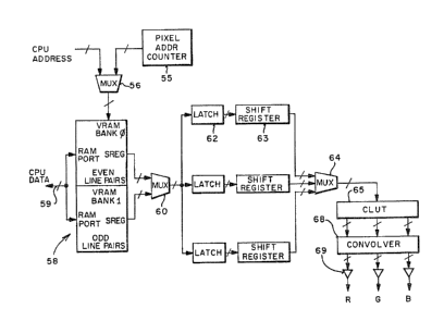
stored in two banks of YRAM memory which together eomprise a frarne buffer. Thisis illustrat~d in Figure 8 by the bank O and bank 1 of memory 68. The addresses for
15 the banks of memory are provided either ~rom the CPU or from a pixel address
counter 55. One o~ these addresses is sel0cted by the multiplexer 56. Data to and
from ths CPU is coupled to the RAM por~s of th~ memory through the bus 59. The
shiR register outpùts o~ either bank O or 1 is seleoted by the multiplexer 60. (This
multiplax~r can ba eliminated if the 3-stat0 f~ature of the VRAM shift register
~0 switches quickly enough.~
Th~ parallel lines from ths multipl0xer 60 are coupled to thr0e l~tches such
as latch 60, and th~n in parallel ~o three shift registars such as shift reglst~r 63. The
multiplexer 64 selects data from ona of th0 thre~ shift regist~rs and couples it to the
color lookup table (CLUT) 65. Th~ oulput of th~ CLUT is coupl~d to a convolver
17
1 320600
such as convolver 68 which may be constructed a~ described above. The digital
olutputs from the convolver ar~ converted by cligital-to-analo~ converters such as
conv~rtor 69 to provide P~GB signals for a color moni~or. Normally, a gamma
correction device is plac~d aft~r th~ convolver 68 in digital or aft~r the conv~rters
5 69 in ana1O9.
As indicated in Figure 8, bank 0 is used ~o store even line pairs of pixel data
and bank 1 is used to stor~ odd line pairs of pixel da~a. Noto this r~ers to "lin~
pairs", not lines th~ms~lvas. More specifically, th~ Weven lin0 pairs~ refers to lines O
and 1, 4 and ~, 8 and 9, etc. The odd line pairs refers to the lines 2 and 3, 6 and 7,
10 etc. The output streams from the two banks of memory (with two-way interleaving~
are rnultiplexed together to form a single word stream as shown in Figur~ 9. This
provides groups of 4 words, one word for each group which is not used. The otherthree words ar~ convolved as describQd above.
An output from bank 0 specifically word 0/lins 0, word 0/line 1, word 1/line 0,
15 and word 1/line 1 is shown in Figure 9. A correspondin~ output frorn bank 1 is also
shown, specifically word 0/line 2, word 0/line 3, word 1/line 2; and word 1/line 3.
After muitipiexing th~y provide a single word stream, speoifically word 0/line 0,
word 0/line 2, word 0/line 1, word 0/line 3, word 1/line 0, word 1/line 2, word 1/line 1
and word 1/line 3. Then, as indicated through convolving, word 0/line 0, word
20 0/line 2 and word 0/line 1 are used to provids data for ~he pixel or pixels
(dep~ndin~ on how many pixels are stored for each word) for line 1 in interlacedfield 1. Similarlyl word 1/line Q, word 1/line 2 and word 1/lin~ 1 provide data for th~
subs~quent pixel or pixels on that lin~. At this time, word 0/line 3 and word 2/line 3
18
1 320600
are ignor~d. On another pass throu~h ihe memory data ~or pixels 7Or line 2 in
int~rlac~d fieJd ? is used; this ~ime word 0/lino 0, and word 1/line 0 are T~nored.
From the viswpoint of the C:PIJ, the VP~AM is mad~ to appear as a
contiguous block. This causes th~ interleavin~ to be ~ransparent to the CPU. Theinterconnections whieh provide this ~ranspar~nce are discussed below.
In the lef~hand column of Figure 10, conv~ntional coupling of the addresses
between 1he CPU and a VRAM is shown. In ~ffect, there is a 1-to-1 connection
b~twccn the CPU address lincs and th~ VRAM address lines. Th~ exampl~ of
Figure 10 assumes a 32-bit word size. Th~ CPU address bits A0 and A1 are thus
10 used to enable VRAM bytes and words, rather than specific VRAM address bits.
For that reasonl the CPU address bit A2 is coupled to tha VRAM address bit A0,
CPU address bit A3 to VRAM address bit A1, etc. Also, since thera are 2 banks ofVRAM, one address lins must ba designated as a bank select signal. With a
conventionai coupling any address bit may b~ used for the convenience of the
15 design. CPU address A19 is shown coupled to BANKSEL in the example.
The connections between the CPU address bits and the VRAM address bits
for the two-way interleaving is shown in the second column of Fi~ure 10. The
exampl~ assumes that there are 1,024 bytes per scan line. If this is the oase, the
address bit A10 from the CPU is the bit which selects between odd and even scan
20 lines. This bit is coupled to A0 of the VRAM. The effect of this bit manipu7ation is
that instead of s~lecting between odd and aven scan lines, the addrGss bit selects
between odd and even words, 1hereby interleaving two lines together by word.
Also, A11 is coupled to BANKSEL to select between VRAM banks 0 and 1 ~very
cther scan line. It is this bit manipulation which makes the two-way int~rleaving
19
1 3~0600
appsar transparent ~o th~ GPU. (It is assumad that the scan line length is a power
of 2, oth~rwisc th~ addr~ssin3 is mor~ complex.)
Th~ shift registers, such as shift register 63 of Figure 8 are used to enabie a
single pixel to be clocked out frorn a word. Typically, more than one pixal is
5 contained in a word therefors a parallel loaded shift register is needed to perrr it the
individual pixels to b0 removed from ~he word. Moreover, if muiti-bit pixels areused, then multi-bit shiR registers are needed for each word.
ALTERNATE EMBODIMENT EMPLOYING FG UR-WAY
INTERLEAVED YRAM
The results described above for a two-way interleavad systern can also be
obtained from a single bank of memory where four-way interlaaving is used. This
embodiment has the disaclvantage that twice the memory capacity is required since
~wo copies of ~he data are needad for the four-way interleaving, as will be
described.
Figure 11 iilustrates a block diagram for the four-way interleave embodiment
which again employs a dual port VRAM memory. The RAM port of the m~mory is
connected through a latch 73 to the CPU to permit data to be r~ad into and r~ad
from the memory. The shift register port of the mamory is coupled ~o thrse latches
such as latch 74 with each latch being coupled to a shift register, such as shift
20 register 75. The multiplexar 76 selects one of the shift regist~rs and oouples its
output to a CLUT 77. A digital color output frorn the CLUT, after convolving by
convolver 78, provides RGB outputs. The latches, shift re~isters, multiplexer, CLUT
and convolver for this smbodiment op~rate in th~ same manner as the embodiment
of Figurc 8 except as discussad below.
~ 320600
Th6 addresses to tha VRAM ar~ selected by the muHiplexer 79 either from
pixel addrQss counter 80 or from the CPU after the C~PU addresses haYe been
coupled to the parallel load counter and latch 81 (as will bs described). Ths rnost
si~niflcant bits of ~he address ars coupled to th~ counter 817 the least significant
5 bits aro simply passed throu~h a latch on~o th~ multiplexsf 79~
As mentioned, a single bank of VRAM is used with four-way int~rleavin~ and
by storing two complete copies of the pixel data in the VRAM 7~. This is necessary
to ob~ain pixel data from three lines (sequentially) and to provide differ~nt
~roupings of lines as will become apparent~ The four-way interleaving causes the10 CPU to write words into VRAM in a 4-line "zig-zag~ order, however, from the CPU's
standpoint this is transparent~ In VRAM each of the two copies of the pixel data is
stored with its interleaving offset by two lines from th~ other copy~ That is, the word
order of the first line of the sven copy is: line 0/word 0, line 1/word 0, lin~ 2/word 0,
line 3/word 0, line 0/word 1, line 11word 1, line 2/word 1, line 3/word 1, etc. And, th~
15 first line of ths odd copy of the frams buffer is line-1/word 0, line-2/wo~ 0, line
01word 0, line 11word 0, line-11word 1, line-2/wor~ 1, line 0/word 1, line 1/word 1,
etc~ (Llnes -1 and lines -2 denote black lines above th~ first line on the display~
Thsy are used to avoid flicker at the perimeter of the display~ They ar~ initially
loadsd with data representing tha color black and ne~d not be accessed by the
20 CPU, once loaded.)
Even though two completo copies of the pixel data are stored in th~ memory,
the CPU only has access to the even copy. When ths CPU writes data into the
msmory, the addresses and data are latched and the write operation is repeated to
write th~ data into the odd copy. Moreover, only the ~ven copy is r3ad by the CPU.
21
1 320600
This additional writing ~or the odd copy is done by ordinary cirouitry in the frarne
buffsr. Th~ even and odd copies are distinguished by the rnost si~nificant bit in the
VRAM, thereby placing the even frarne copy in the lower half of the memory and the
odd copy in the upper half.
The four-way interieaving ~r the even copy is obtained by taking the
address bits from the CPlJ which select between odd and even scan lines and
conneoting them to bit 0 of the VRAM. Ths addrsss bit from the CPU which selectsbstwean cven and odd soan line pairs is connected to bit 1 of ths VRAM and thsn
all other bits from ths CPU are shifted "upward as shown in Figure 13 in ~he
righthand column. Again, in Figure 13 the conventional interconnecl is shown in
the leflhand column for purposes of comparison as it was in Figur~ -0. The eff0ct
of this bit remapping for the 1024 bytes per soan line display is that the odd and
even scan line ~bit" (e.~., bit 10) selects between ocid and even words, and the odd
and even scan line pair bit (e.~., bit 11 ) selects between odd and even wQrd pairs.
1~ From the CPU's viewpoin~, onca again, the memory appears as a contiguous block.
The four-way interlsaving for tha odd ~rame buffer copy is obtained in ths
same mann~r as the ~ven copy, axcept that before the bit remapping an add0r
adds the length of two scan lines to the address generated by the CPU ~for
example, for 1024 bytes per scan line, th~ number 2048 is added to th0 CPU
address prior to the bit rsmapping). The effect of this addition is to oHset thecontents of the odd copy in the buffer by two scan iines (i.e., after remapping by 2
words). (It is assumed the scan tin~ 10ngth is a power of 2, otherwise addr~ssing is
more complex.)
22
1 320600
The two scan line addsr is easily impl0manted since the only time th~ odd
bank copy is addrassed is a~ter the even copy has been addressed. This addition
is obtained from thB coun~er 81 of Figur~ 11 by incrementing the counter. Assum~that th~re ar~ 1024 bytes per scan line, than the CPU address bits A0-A10 are
5 latched in ths latch of counter and latch 81, and ths address bits 11 and higher ar~
coupled to the counter. To wnte the even eopy tha address bits ar~ simply latched
by the countsr and la~ch 81. To write tha odd copy, the counter is incremented and
the data which has been latched is written into the memory with a two scan line
offset.
Another effect of ~he address manipulation is to cause ths output of the
memory (shiR register port) to be in scan lines of ~line quads". The sven line quads
ars 0/1/2/3, 415~17, 819/10~11, etc. The odd line quads are -2/-1/0/1,2131415, 6171819,
etc. Each convolution triplet needed by the convolver is then available in on0 of
the~e line quads. The line quads are sequenced in the sams ordar for both ~ields:
15 cdd lina quad -~-1/0/1, even line quad 0/1/213, odd line quad 2131415, even line
quad 4/51617, etc. The particular field displayed is determined by which three lines
are convolved from each line quad. For example, in field 1 for lines -1, 1, 3, and 5
th~ tripies -2/-1/0, 0/112, 21314, and 41516 are needed. Then in field 2 for lines 0, 2,
4, and 6 the tnples -1/0/1, 1/213, 31415, and 516n are needed resulting in the same
20 line quad sequence.
The output of the memory is latched and then the shift registers ars used in
the manner described in conjunction with the previous embodiment, except that the
line order and the line quads is different, this difference being shown in Fi~ure 12.
23
~ 320600
E;OFTWARE EM130DIMENTS OF THE PRESENT INVENTIC)N
The method of ~h~ present inv~ntion can be raadily impl~menl~d in so~war~
to provid0 real tim~ csnvolution. Two ~rnbodiments of the inv~ntion ar~ described
bQlow, one, ~or a planar frame buffer and ~he other for a "chunkya frame buffsr. The
5 mathod for the planar frame buffer is par~icularly useful where a single bit per pixel
(e.g., indicating black or whit~) is stored in the buffar.
A planar fram~ buff~r for purposes of this applica~ion (as well as being the
g~nsrally accepted d~finition), is one made up o~ bit planes, where aach plan~
providas one bit for each pixel of the display. This arrangemcnt is used in
10 numarous commercially available computers such as those manufacturad by Sun
Microsystems, Inc., Apollo, SGI, etc. To specify a color for a given pixel, each plane
contributes one bit. Thus, if ther~ are eight planes, the maximum color depth is 8
bits pQr pixel; if there ars 24 planes, the maximum color depth is 24 bits per pixel,
QtC. The CPU accesses words in a pianar frame buffer only one plane at a tim~.
15 For Qxample, a 3~-bit read or write from th~ GPU would allow access to one bit of
32 horizontally adjaccnt pixels at once. For the CPU to acc~ss all bits in a single
pixQI, it must perform as many access cycles as there are planes.
In contrast, with a chunky ~rame buffer, all the bits for a given pixel are stored
as adjacsnt bits o~ a m~mory word. For ~xample, if color depth is 4 bits p~r pixal,
~0 and lhc CPU word size is 32 bits, then 8 pixels ar~ stored in each CPU wnrd.
UnlikQ thQ planar frame buffer, a given CPU access will always access all the bits
in a givsn pixel, and in some cases, ~he bits in adjac~nt pixels. Chunky frame
buffers are also used in commercially availabl~ computers such as Appl~
Computer, Inc.'s Macintosh 11 cornput~r.
~ 320600
A. Software Embodlmen~ of the Present InVQntlOn for a Plan~r Fr~3ms
BulFf~r
Assume a on~ bi~ p~r pixel display is stored in the frame buffer, for cxample,
in plane 0. Referring to Figure 1 q, and i~noring for a mom~nt, s~ep 83, srdinary
5 block moves are empioyed to mov~ tho pixel data from plans 0 to pl~n~ 1,
howsver, when this data is moved into plan~ 1, it is plaoed on0 scan lin~ down as
shown by block 84. Th~ data is again block moved from plane 0 to plane 2 of the
buffsr, but this time when writing into plane 2, it is written one scan line up when
compared to plane 0 as indicated by step 85.
As indicated by step 86, the data from planes 0, 1 and 2 is scanned out of
the memory. The block moves assure that the proper bits are available in bits 0, 1,
and 2 of each pix81 to immediately do a convolution as desoribed above (typically
a "1-2-1~ convolution). For any ~iven pixel, plane 0 contains the line n bit, plane 1
contains the line n-1 bit and plane 2 con~ains the line n+1 bit.
In the currently preferred embodiment of this method, the convolution is, in
affect, precomputed for each possible 3 bit combination output from ths m~mory
and is storad in a color lookup table. This is shown by the first step 83 where the
CLUT is preloaded with a gray scale data. Tha output of the memory during
scanning is coupl~d to the CLUT and tha output of the CLUT providcs tha
20 convolved pixel data as shown at step 87.
This ombodimant is again illustrated in FiQure 15 where it is assumed that
thc planar frame buff~r has 4 planes, plan~s 88, 89, 90 and 91. In typical
opsration, the four bits defined in each pixel are provided one from ~ach plane, as
shown within the dotted line 92. Also, during typical color op~ration, th~ 4 bit
1 320600
outpu~ ~rom th~ buffer is coupled to th~ color loo~up table 93 to, ~or exampl~, ;
provid~ a 12 bit RGB output.
When the method of tho present invention is implemented, a orle bit per
pix61 display is stored in plane 0. At system startup th~ ~ight ontries of the CLUT
5 (since thsr~ ar~ thr~ bits per pixel, thsr~ ar~ ~ ~ntries) load~d ~o th~ ~abl~ of gray
scales (see Figure 21). Then, the CPU rep2atedly does block moves of th~
entir~ty of plane 0 to planc 1, however, one scan line down. The data from block 0
is also moved to block 2, ~his tim0, on~ scan lin~ up. Once this is done, th~ data
~rom the planes 88, 89 and 90 is coupled to the color lookup table to provide the
10 gray scal~ output. (The data, if any. from plane 3 is ignored for this mode.)Steps ar~ taken to prevent flickering at ~he edge o~ the screen or display, thatis, to prevent abnJpt transitions at the top and bottom. It is generally best to have
the border of the display smoothly convolve into black at th~ top and bottom. This
is achieved by allocatin~ one line initialized to black at the top and bottom of plane
15 0, two iines at the top of plane 1 and two lines at the bottom of plane 2. These
~guardbands~ assure that the top and bottom borders are smoothly convolved to
black.
In the currently preferred embodiment, gamma correction is used as shown
by block 13 of Figure 1. The gamma correction can be built into the gray scal0 data
20 and hence, loaded into the CLUT on inilialization.
In a typical application, ths CPU may not be fast ~nough to complete the
block movcs to planes 1 and 2 in a single frame Ume. It has been found that it is
visually acceptable to complete the block moves in several frame times since plane
26
1 32()600
O is always up-to-dat~ and it contributes on~-half of th~ int~nsity for a ~iv~n pix~l
vaiue.
27
1 320600
13. Sottwsra Embod~ment for the Chunky Frame Bu~fer
In this embodiment, a one bit per pixel real-time convolution with a chunky
fram~ buffar is r~alizad. Unlike tha method described abov~ ~or the planar ~ramebuffer, the ~xact numbsr of bits per pixsl cannot be ob~ained whsn rearranging the
5 data, hence, ~he next power of 2 ~reater than ~he number of bits needed is used.
For the described embodiment, thr~e-lines are used for the convolutisn and hence,
four bits of pix~l are s~ored in a buffer for each pixel. Th~ mathod described b~low
places th~ bits in their proper position.
First, H should be noted that a one bit per pixel frame buffer "off scre~n" in
O RAM is used by the CPU for drawing. This frame buffsr is separate from the four bi~
p~r pixel frama buffer that is ac;ually scanned to provide ~h~ display. Tha method
described below reads data from the one bit per pixel frame buffer, expands the
data to th6 four bits per plxel, ~hen writes ~he data into the four bit per pixel frame
buffer. The method merges the pixel information from tha two previous lines before
15 it writes tha results into th0 four bit per pixel frame buffer. When the four bit pixel is
presanted to th~ color lookup tabla, the three bits for lines n-1, n and n~1 areavailable to lookup th~ proper gray scale for the 1-2-1 convolution. Again, as with
the pravious ambodiment, the color lookup table is loaded with ~ray scale
information to provide the convolution. (Thr~e of the four bits read from the four bit
~O par pixel fram~ buffer are used by the CLUT to provide the output convolvad signal
for tha display.)
Step O
Four 32-bit words (A, B, C, and D) ars initialized to zero. (A, B, C, and D
oaoh refer to 32-bit registers within the CPlJ.) A 32-bit word R is raad starting from
28
1 320600
ths laRmost pixel position of the top scan line of ths one bit par pixel ~rame buffer.
A B, C and D ara ali stored a~ adjacent laf~ to right locations starting from tha ~op
scan lins of the four bit psr pixel frame buffer.
Step 1
R is read from th~ next 32 bits in ths ons bit per pixel fram~ buffer
immediately below the last 32-bi~ word read from the one bit per pixel frame buffer.
This is shown in Figure 16 where two words, words 93 and 94, are shown ~or linesn and n~1 in the ons bit per pixel frame buffer.
~;t~p ~
As shown in Figure 17, one byte of R is expanded into a second 32-bit word
M such that sach of the 8 bits is placed at 4 bit intervals in the 32-bit word starting at
bit 1 (i~e., bit 0 to bit 1, bit 1 to bit 5, bit 2 ~o bit 9, etc.~ and a 1 is placed in every 4th
bit startin~ at bit 0. All o~her bits are set ~o zero. For example, the byte 0111 0101
is converted to (shown as groups of 4): 0001 0011 0011 0011 0001 0011 0001
0011. This is dona by using a 256x32-big pre-loaded lookup taùle in RAM.
Step 3
A is leR-shifted by 1. In some microprocessors such as the Motorola Part No.
68020 this can bà accomplished mors quiokly by adding A ~o itself. In the upper
part of Figure 18, A is shown before the shift and in the lower part of Figure 18 after
tha shift.
Step 4
M is bit-wise ORed into A as shown in Figure 19. First, this serves to merge
th~ byte from R into A since it is known that the bits in A corresponding to the bits
from the byte from R are all zero (anything-ORed with zero retains its value).
29
.
'' :` ' :
.
1 320600
Second, this serves to for~e every 4th bit starting with bit 0 in A to one (this sets up
for tho merg~ operation in s~ep 10, below).
S~ep ~
A is stored in th~ ~our bit per pixel fram~ buff~r immediately below ~hs last
5 plac~ A was stor~d as shown in Figur~ 20.
~;t~p 0
Steps 2 through 4 are repeated for the thre~ other bytes from R. This time,
however, B, C, and D ars usad instead of A.
Step 7
R is read for the next 32-bit word in the one bit per pixel franne buffer
immcdiately below the last 32-bit word as in Step 1 above.
Step 8
As shown in Figure 17, one byte of R is ~xpanded into M with each of th~e
eight bits placed at 4 bit intsrvals startin~ at bit 1. Also, a 0 is placed in CVQry 4th bit
15 starting at bit 0 and all other bits ara set to 1. For exampl~, the byte 0111 0101
would be converted to 1100 1110 1110 1110 1100 11101100 1110. This is
accomplished by means of a second 256x32-bit pre-loaded lookup tabl~ in RAM.
Step ~
As shown In Figurs 18, A is left-shifted by 1. Once again, as mentioned for
20 step 3, addition of A to itself may be used.
S~ep 1 0
As shown in Figure 19, M is bit-wise ANDed into A. First, this serves to
merge tha byt~ from R into A since it is known that the bits in A corresponding to the
bits from the byte from R ara all on~s (anything ANDQd with on~ retains its vaiue).
1 320600
Second, this serves to force ~very 4th bit starting with bit 0 in A to zero (this will set
up the merge operation in step 4, above).
Step 1 ~
A is stored in th~ 4-bit frame buffer immediately below the last place A was
5 stored. See word 95 of Figure 20.
Step 1 2
Steps 8 through 10 are repeated for the 3 other bytes from R. They are
me~ged in B, C, and D instead of A. See words 96, 97 and 98 of Figure 20.
Step ~3
Steps 1 through 12 are repeated until the bottom of th~ frame buffer is
reached, then R is read for the pixels on the top scan line of the 1 biVpixel frame
buffer just to the right of where it was loaded at the start of the last pass. A, B, C,
and D are all stored at adjacent left-to-right locations on the top scan line of the 4
biVpixel frame buffer just to the right of wher~ they were loaded at the start of thc
15 last pass.
In summary, th0 pixels in the 4-bit per pixel frame buffer 100 of Fi~ure 20 are
coded with line n+1 in bit 1, n in bit 2, and n-1 in bit 3 (this resulting bit configuration
is shown in Figure 19). ~it 0 is i~nored by th~ CLUT 101 of Fi~ure 20. The on~ bit
per piXQI frame buffer of Fi~ur0 16 is scanned vertically with a new bit added into
20 oach four bit pixQI for each scan line by left shifting the existing bit for th~ pix~l by
one and merging the new bit into bit 1 of the 4-bit per pixel word. The shift
op~ration serves to adjust th~ pixel from its previous centering on lin6 n-1 (the line
above) to its current centaring on line n. In other words, when th~ operation begins
the four bit pixei data contains bits ~rom lines n-2, n-1 and n since the data was
.
1 320600
used for the line abova. The left shif~ operation changes the configuration of the
four bits to n-1, n, and a ona or a zero in bit 1 (bit 0 is ignored). Than, the new bit
from the one bit per pixel frame buffer is merged into bit on0 for line n~1. The new
assembled four bit word is stored in the four bit per pixel frame buffer and as
mentioned, the CLUT is used ~o provide th3 convolution.
In detail, the method star~s in the upper-left of the fram~ buff0r and works
down a 32-pixel column. The read into R loads the 32 1 bit pixels then each 8
pixels of the 32 are operated upon ~eparately. Th~ tirst 8 pixels (a byte) ar~ used
as a lookup table index to fetch a 3~-bit word, M. M holcls the 8 pixels, spread out
10 at 4-bit intervals so that they are ready to merge for ~ha 4 biVpixel frams buffer.
M also is set up with the rest of its bits prepared for eithsr a bit-wise AND
merge or an OR mer~e. The reason it alternates between AND and OP~ is that i~
saves the step of clearing (or setting) th~ bits in A which are th~ destination for the
8 pixels from R. Since A will be left-shifted just prior to the AND or OR mer~, th~
15 bit immediateiy to th~ right of the destination of th~ R bits is ~orGed so that at the
next step they are already prepared for merging. AND prepares for th~ OR by
forcing zeroes, and OR prepares for ths AND by forcing onas.
A is lefl-shiRed by one to update th~ pixei from being centered for the
pr0vious line to being centered for the current line. Th~ leR-shift moves the
20 pr0vious line n~1 to the current line n and the pr~vious line n to ~he curr~nt lin~ n-1.
Previous line n-1 (current line n-2) is shifted out. Notice that this shift applies to all
aight pixols contained in the 32 bits of A so it is an 8-way parallel op~ration. Notice
also the bits from previous line n-1 shifts into the unused bit of th~ next 4-bit pixel to
the left (or off tha left edg~ of the 32-bit word).
32
1 320600
Than, M is merged with A by ~ither an AND or an OR. Bits from n and n-1
ara left alone, new n~1 bits are merged in, and the unused bits are set to knownstate (0 if an AND, 1 if an OR). A is finally stored in tha 4 biVpix~l frame buffer.
The other 24 pixels in R are handled the same way, with 8 pixels each for B,
5 C,andD.
The same steps ar~ performed for ~ach SUCCeSSiVQ scan line below until ths
bottom of the frams buffsr is reached. Then, the next column of 32 pixols
immediately to the right is scanned-down, and so on until the entire frame is
scanned.
10The CLUT 101 of Figure 10 is loaded in a similar manner to that of the
planar frame buffer implementation above shown in Figure 21. The diffsrflnces are
that the bit ordering is different and that since bit 0 in the 4-bit pixels is
indeterminate (it alternates depending on whether tha last mer~e was with an ANDor an OR), the same gray value for every two CLUT ~ntries is stored.
15OTIIER CONVOLUTION KERNE~ S
In the previous section, most of the emphasis has bsen on thc 1-2-1 kernel.
Experiments have shown that neith~r a 3-line convolution nor on-off-on-off
reduction of 50% gray is assential in all situations for effe~ive interlace flicker
r~duction. If the constraint that on-off-on-off horizontal line patterns are reduced to
20 a 50% gray is maintained and other kernel sizes are tried other than 1 x3, for each
k~rnel size there is one set of coefficients to meet the on-off-on-off constraint.
ThssQ coefficients match Pasqual's triangle (i.e., 1; 1, 1; 1, 2, 1; 1, 3, 3, 1; 1, 4, 6, 4,
~; QtC.)~
1 320600
ADAPTIVE CONVC)LLITION
As mentioned above, the worst flickQr patterns are the ones which have hi~h
hori~ontal coherence ~i.e., repeat horizontally). Horizontal solid lin~s, hsrizontal
dashed lines, and gray dither patterns ar~ examples of patl erns with high
5 horizontal coherence. Taxt is an exampl~ of patterng without such cohsr4nce. The
~nvolution discussed above may be adaptive, that is, it may be varied depending
on the type of patterns bein~ displayed. First, it is determined whether a repeating
pattern is occurring in a local horizontal group of kernels, for ~xample, 8 pix~ls
across. If there is a panern in the kernels, th~n all of th~ kernels are convolved, for
10 example, with the 1-2-1 coefficients. If ther~ is no such pattern, then the 8 pixels
are convoived with coefficients making a sharper filter ~e.3., 1-3-1 or 1-~4-1 )o The
test to determine whether a pattern is repeating must be applied continuously in a
moving horizontal window, kemel by kern~l. Sino~ the test windows ov~rlap, some
kernels may be part of a pattern in one test window but not in ano~her. For ~hese
15 kern~ls, the 1-2-1 oonvolution is us~d, since they are at the edga of the pattern.
Different lests may be used for determining whelher a pattern is b~ing repeat~d, for
example, 1h~ left four ksrn01s may be oompared with the right four kem~ls withintha window.
34