Note: Descriptions are shown in the official language in which they were submitted.
~ 2 ~ 9 ~ 3 667~2-296
CROSS REFERENCE TO COMMONLY
ASSIGNED COPENDING APPLICATION
Reference is made to Canadian Patent Application
Serial No. 544,546 by Baudino at al for an "Oxygen Sensing
Pacemaker" filed August 14, 1987.
BACKGROUND OF THE INVENTION
The present invention relates to cardiac pacing
generally and in particular to a cardiac pacemaker which reg-
ulates pacing rate based upon sensed percentage of oxygen sat-
uration of the blood.
The relationship between oxygen saturation of theblood and pulse rate in a healthy heart is well known. This
relationship has given rise to numerous proposals for pacemakers
which regulate pacing rate in response to sensed blood oxygen
level. These pacemakers attempt to restore the natural relat-
ionship between blood oxygen level and pulse rate in order to
provide a pacemaker which paces the heart at a rate appropriate
to the physiological demands of the patient's body.
An early proposal for such a pacemaker is set forth
in United States Patent No. 4,202,339, issued to Wirt~feld et al.
This pacemaker takes the form of an asynchronous pacemaker which
does not sense the heart's underlying electrical activity.
United States Patent No. 4,467,807, issued to sornzin discloses
,~
, :.i ' ' . ~ . ' , ! . .
' '. : ' , ' .' '' ' ~ ' ' ~ . "
~ , ~. i ~" . ,
- 1 13 2 9 9 3 66742-296
a pacemaker in which the oxygen sensor's function is integrated
with a sense amplifier for sensing intrinsic heart activity.
This approach is believed superior to that of Wirtzf~ld in that
it avoids competing with underlying heart activity and allows
the heart to beat at its own, underlying rhythm if that under-
lying rhythm is appropriate.
, . ' .:
: .
~ 3 ~ 3 66742-296
SUMMARY OF THE INVENTION
The present lnvention provldes a reflned version of an
oxygen senslng pacemaker ln which the oxygen sensor ls mounted on
the paclng lead. The o~ygen sensor requlres only two conductors
for operatlon, yet includes a two wavelength reflectance oxlmeter
for lncreased accuracy. ~xperlence in the Eleld of cardiac paclng
has shown that one of the more vulnerable portlons of the pacing
system ls the pacing lead, whlch ls exposed to mechanlcal stres-
ses. Therefore, lt ls felt that the simpler the structure of the
paclng lead ls, the more rellable and durable lt ls likely to be.
In additlon, reduclng the number of conductors to two allows for
easier lnstallatlon of the pacemaker and lead and allows the use
of standard bipolar pacemaker and lead connector conflguratlons.
For these reasons, an oxygen sensor requlring only two conductors
ls belleved deslrable.
The sensor and clrcultry are also conflgured to mlnlmlæe
the current draln lmposed by the sensing reglme, whlle retalnlng
the hlgh degree of accuracy and llnearlty provlded by a two wave-
length reflectance oximeter. The sensor lncludes an oscillator
which se~uentially activates red and lnfrared diodes. The activa-
tlon times of the infrared and red diodes are determlned by the
amounts of lnfrared and red llght reflected by the blood. The
sensor draws substantl~lly more current when the red diode ls
activated than when the infrared diodes are actlvated. This
allows the pacemaker to measure the duratlons of the red and
infrared diode actlvation perlods. Thls approach provldes a
slgnal to the pacemaker whlch has hlgh resolution, lncreased nolse
lmmunity, and ls less affected by long term fluld inflltratlon
lnto the paclng lead. The lntermlttent operatlon provldes a
deslrably low current drain.
~, .
- : .: ,. :
. -
. '
~32~9~3 6~742~296
Thus, in accordance with a broad aspect of the
invention, there is provided a cardiac pacemaker of the type
comprising pulse generatiny means for generating cardiac pacing
pulses, timing means coupled to said pulse generator means for
causing said pulse generator means to generate said pacing
pulses at controlled intervals, and a cardiac pacing electrode
coupled to said pulse generator for applying said pacing pulses
to the heart, wherein said pacemaker further comprises sensor
means for sensing the percentage of oxygen saturation of the
blood, said sensor comprising:
red light source means for generating red light;
infrared light source means for generating infrared
light;
oscillator means for sequentially activating said
infrared light source means for an infrared activation period
and for activating said red light source means for a red act-
ivation period;
means for allowing said red and infrared light
generated by said red and infrared light sources to exit said
sensor and impinge upon the blood and to allow said red and
infrared light reflected by said blood to reenter said sensor;
light sensing means for sensing said red and in-
frared light reentering said sensor body and for regulating
said red activation period and said infrared activation period
.
~ , ,
9 ~ 3
-2b 66742-296
dependent upon the amount of said red and infrared light
reflected by the blood; and
means for applying a power signal to said sensor;
and
wherein said sensor means modulates said power
signal applied to said sensor means in accordance with said red
activation period and sa.id infrared activation period;
and
wherein said pacemaker further includes monitor
means for monitoring said modulated power signal applied to
said sensor and for determining the relative durations of sald
red and infrared periods and a timing adjustment means coupled
to said monitor means for adjusting the time interval of said
pacing pulses generated by said pacemaker in accordance with
the relative durations of said red and infrared periods.
- . . .
: - :
: . : : , . .......................... .
~,
9 ~ 3
3 66742-~96
BRIEF DESCRIPTION OF THE DRAWINGS
Fig. 1 is a block diagram lllustrating the functlonal
relatlonshlp of the ma~or elements of the pacemaker.
Flg. 2 ls a tlmlng dlagram lllustraklng the basic
timlng of the pacemaker.
Flg. 3 is a graph lllustratlng the correlatlon between
the paclng rate provlded by the pacemaker and the percentage of
oxygen saturatlon.
Flg. 4 ls a sectlonal drawlng of the assembled oxygen
sensor.
Fig. 5 ls a plan view of the top of the hybrld clrcult
withln the sensor.
Flg. 6 is a plan vlew of the bottom of the hybrld clr-
cult withln the sensor.
Fig. 7 ls a schematlc of the hybrld clrcult wlthin the
sensor.
Fig. 8 is a timing dlagram lllustratlng the operatlon of
the sensor and associated clrcultry.
F'lg. 9 1s a tlmlng dlagram illustratlng the operatlon of
clrcultry whlch decodes the slgnals provlded by the sensor to pro-
vlde a signal lndlcatlve of oxygen saturatlon.
Flg. 10 ls a schematlc of the pacemaker.
DETAILED DESCRIPTION OF THE DRAWINGS
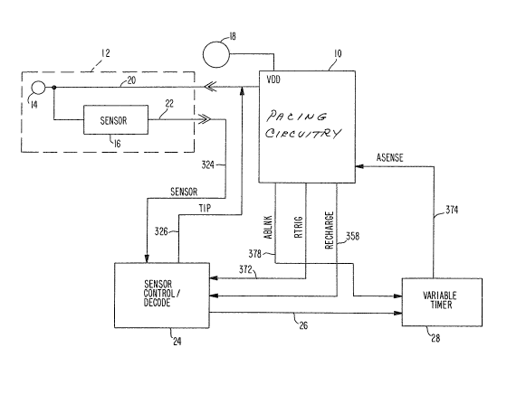
Fig. 1 is a block diagram of the primary components of
the pacemaker~ Basic operatlon of the pacemaker 15 described in
con~unction with the tlmlng dlagram in Flg. 2.
The pacemaker ls based upon a VDD pacemaker of the type
known to the art. Such a pacemaker typically lncludes a ventrl-
cular pacing electrode, an atrlal amplifler and a ventrlcular
amplifier, whlch sense electrlcal actlvlty ln the atrlum and
v0ntrlcle of the heart, respectlvely. In the present embodlment,
the atrlal ampllfier is dispensed with. However, all tlmlng
clrcultry assoclated wlth the atrlal ampllfler ls retained. In
~",
.
4 667~2-~96
the present embodlment, the VDD paciny clrcultry 10 is taken from
the Enertrax~ pacemaker, manufactured and sold by the asslgnee of
thls appllcation. However, other VDD or DDD pacemakers would
provide a sultable startlng polnt, provlded they have at least the
lnputs and outputs dlscussed helow. A more detalled descrlptlon
of such pacemakers can be found ln U.S Patent No. 3,6~8,707 lssued
to Greatbatch and U.S Patent No. 4,059,116 lssued to Adams.
The baslc operatlon of a VDD pacemaker is well known to
those skilled ln the art. l'ypically, ln response to a sensed
atrlal contractlon, the clrcuitry lnltlates timing of an A-V
lnterval. If no ventrlcular contractlon is sensed during the A-V
lnterval, a ventrlcular pacing pulse ls generated. After a sensed
ventrlcular contractlon or a ventrlcular paclng pulse, if no
underlylng atrlal or ventrlcular actlvity occurs wlthin a pre-
determlned V-V lnterval, a ventrlcular paclng pulse is generated.
In the present invention, the atrial amplifier ls dlspensed with,
and the sensor and assoclated clrcultry provlde a slgnal whlch the
pacing clrcuitry treats as lf lt were a sensed atrlal contractlon.
By varylng the tlmlng of thls slmulated atrlal contractlon, the
underlylng pacing rate of the pacemaker ls controlled.
The paclng c.Lrcultry ls coupled to the heart by means of
a paclng lead 12 whlch lncludes a tlp electrode 14 and the sensor
16. Paclng occurs between the tlp electrode 14 and the can 18 of
the pacemaker. Senslng oE ventricular activlty also occurs be-
tween the tlp electrode 14 and the can 18 of the pacemaker. The
lead 12 has two conductors 20 and 22, coupled to the paclng clr-
cultry 10 and to the sensor control/decode clrcuitry 24, respect-
lvely. Sensor control decode clrcuitry 24 provldes a slgnal on
line 26 indlcatlve of the sensed oxygen saturatlon percentage.
The operatlon of the pacemaker can best be understood in
con~unctlon wlth the timlng dlagram ln Flg. 2. The ~CG trace
lllustrates the electrocardiogram of a patlent ln whlch a pace-
maker accordlng to the present lnventlon has been implanted. The
first QRS complex 50 :Ls a natural ventrlcular contractlon sensed
. .
'
~ ~ h ~ ~ ~3
6~7~2-296
by the paclng circuitry lO. The sensed contractlon causes genera-
tlon of a pulse 52 on RTRIG line 372. Sensing of the ventrlcular
contraction also lnltlates an atrlal blanklng perlod whlch pre-
vents the pacer from respondlng to electrlcal signals ln the
atrlum. Durlng the atrlal blanklng perlod, a low loglc slgnal 54
is generated on ABLNK llne 378. The atrlal blanklng signal ex-
tends until 120 ms following the sensed ventrlcular contractlon.
The varlable timer 28 (Flg. l) lncludes an RC tlmlng
clrcult controlled by ABLNK llne 378 and by the slgnal lndicatlve
of o~ygen saturatlon, provlded by the sensor control decode clr-
cultry 24 on llne 26. Variable timer 28 begins tlmlng a varlable
delay interval on expiration of the atrlal blanklng perlod at 56.
Upon time out of the variable delay lnterval at 58, timer 28
generates a slmulated atrlal sense slgnal 60 on ASEMSE llne 374.
The slmulated atrlal sense slgnal 60 causes the VDD
clrcultry 10 (Flg. l) to initiate the tlmlng of the A-V interval
at 62. In addltion, the slmulated atrlal sense slgnal 78 causes
the pacing clrcuitry 10 to inltiate th~ atrial blanking period,
drivlng ABLNK llne 378 low at 64. At the explratlon of the A-V
interval at 66, a ventrlcular paclng pulse 67 is generated, caus-
ing a posltlve slgnal 68 on RECHARGE llne 358. At the explratlon
of the atrlal blar,klng lnterval at 70, tlming of the variable
delay is reinitlated at 72. Thus, the interval between a sensed
contractlon 50 and the next subsequent ventrlcular pacing pulse ls
determlned by the sum of the A-V lnterval plus the varlable delay
lnterYal determlned by varlable tlmer 28 plus 120 ms. The
duratlon of the varlable delay lnterval ls determlned by -the slg-^
nal on line 26 from the sensor control/decode clrcuitry 24.
The escape lnterval followlng a ventrlcular paced beat
ls determined ln a simllar fashion. Followlng the paclng pulse
67, the atrlal blanklng perlod remalns ln effect for a perlod of
120 ms. Upon e~plratlon of the atrlal blanklng perlod at 70,
varlable tlmer 28 reini.tiates timlng of the varlable delay
lnterval at 72. Tlme out of the variable delay interval at 74
1 ~0~3
~ 667~2-29
trlggers the generatlon of slmulated atrlal sense slgnal 76 on
ASENSE line 374. Th1s in turn inltiates tlmlng of the A-V lnter-
val at 78, and lnltlate~ the atrlal blanking perlod at 80, driving
ABLNK llne 378 low. At the e~piratlon of the A-V lnterval at 82,
a ventricular paclng pulse 84 ls generated followed by a corres-
pondlng posltlve slgnal 86 on R~CHARGE line 358.
Sensed ventricular contractlon 94 follows pacing pulse
84 by an lnterval less than the sum of 120 ms plus the A-V dela~
plus the varlable delay. Thls termlnates tlmlng o~ the A-V inter-
val at 96. The atrlal blanklng perlod lnitiated at 98 by time out
of the variable delay at 99 will termlnate at 100, 120 ms follow-
lng sensed ventrlcular contraction 94. At that tlme, tlming of
the varlable delay ls relnitlated at 102. A posltlve going signal
on RTRIG llne 372 correspondlng to sensed beat 94 ls lllustrated
at 104.
Pacing clrcultry 10 also lncludes a V-V tlmer. As dls-
cussed above, thls tlmer sets a mlnlmum pacing rate. Thls timer is
lnltlated concurrent wi.th elther sensed ventrlcular contractlons
or ventrlcular paclng pulses. In the examples of Flg. 2, the V-V
timer is inltiated at 88, 90 and 92. Because the total of 120 ms
plus the A-V delay plus the variable delay was less than the
underlylng V-V lnterval, the V-V timer does not time out in Flg.
2. However, ln the event that the sum of 120 ms plus the varlable
delay plus the A-V delay were greater than the V-V interval, pac-
lng would occur on the explration of the V-V interval.
In summary, the pacemaker operates slmilarly to the
pacemaker disclosed in the Bornæln patent referred to above, in
that the escape lnterval following elther a sensed ventricular
contraction or a paced ventricular contractlon ls determined by
the sensed oxygen saturatlon percentage. Like the pacemaker
descrlbed ln the Bornzln patent, senslny of natural ventricular
contractlons prlor to the explratlon of the escape lnterval re-
lnltlates timing of the escape interval.
The signals on RECHARGE llne 358 and RTRIG line 372
.
.. ,
7 ~32~3 667~-296
are provided to the sensor control/decode clrcultry 24 where they
are counted. After every fourth count, the sensor 16 ls activa-
ted, and a new value of oxygen saturation ls decod~d by clrcuitry
24. This slgnal indlcative of the percentage of saturation ls
provided to variable tlmer 28 on llne 26, and the variable delay
interval ls correspondlngly changed.
Fig. 3 illustrates the various relatlonships between
oxygen saturation and pulse rate available ln the pacemaker. The
pacemaker provldes ~wo sets of curves relating oxygen saturation
and pulse rate, which are referred to herea:Eter as family A and
famlly B. As dlscussed above, the paclng rate is the sum of the
A-V lnterval, the 120 ms atrial blanklng perlod followlng ventrl-
cular pace or sense, and the varlable delay lnterval determlned by
the varlable timer 28. In the particular VDD pacing circuitry
utlllzed, that of the Enertrax~ pacer, there are ten avallable A-V
intervals ranging from 25 ms to 250 ms ln 25 ms increments. These
control settlngs determine the curves wlthln farnily A and famlly
B. For example, the curves lllustrated as A10 and ~10 employ an
A-V lnterval of 25 ms, whlle the curves lllustrated as Al and ~1
employ an A-V interval of 250 ms.
The sensor/control decode loglc 24, Flg. 1, provides an
output slgnal on llne 26 which is proportlonal to the sensed
oxygen saturation. The specific relationship between sensed
oxygen saturatlon and the outpuk signal on llne 26 ls ad~ustable
between two settlngs whlch deflne the A and B famllles of curves
illustrated in Flg. 3. At any partlcular sensed oxygen saturation
percentage, the varlable delay lnterval in the B family is about
one-half of the correspondlng variable delay ln the A famlly.
This provldes lncreased flexlbllity to optlrnize the pacemaker's
operat ion for the partlcular patlent ln whlch it ls implanted.
Withln ea~h famlly of curves, any oi- the 10 A-V lntervals may be
selected to produce a total of 20 posslble response curves. The
speclflcs of the operatlon of sensor control/decode clrcultry 24
and variable timer clrcuitry 28 are dlscussed in more detail below
,
~2~3
8 66742-236
in con~unctlon wlth the dlscusslon of Flg. lO.
All curves lllustrated employ an underlying, V-V lnter-
val of 1500 ms, correspondlng to 40 beats per minute. Thls lnter-
val ls also programmable and determlnes the lowest available pac-
lng rate. As discussed above, unless the sum of the A-V delay,
the varlable d~lay and the 120 rns post ventrlcular atrlal blanklng
interval ls less than the V-V lnterval, paclng wlll occur on ex-
plratlon of the V-V lnterval.
Flg. 4 ls a sectlonal drawlng of the assembled sensor
ready for lncorporatlon ln a cardlac paclng lead. The sensor
lncludes a machlned sensor body 200 which may be fabrlcated of
tltanium. The sensor body 200 serves both as a structural element
and as a conductlve element. The dlstal end 202 of sensor body
200 ls provided wlth a bore 204, ln which a colled conductor
coupled to the tlp electrode 14 (Fig. 1) of the paclng lead 12
(Flg. 1) may be mounted. The proxlmal end 206 of sensor body 200
ls preferably coupled to one of the two elongated conductors 20
and 22 (Fig. 1) ln the paclng lead 12. The sensor body 200 thus
serves as part of the conductor coupllng the pacemaker to the tlp
electrode. A wlre 208 enters the proxlmal end of the sensor body
200 vl~ bore 210. Bore 210 ls sealed by means of feed through
212, whlch may be fabrlcated of sapphlre and is provided wlth a
metal sheath 213 whlch is welded to æensor body 200.
Sensor body 200 serves to mount the hybrld clrcult 214,
whlch contalns the active clrcult elements of the sensor and ls
provlded wlth a central bore 201 to allow access to the bottom of
hybrld circuit 214. The circultry of hybrid clrcult 214 ls coup-
led to the sensor body at lts dlstal end by means of strap 216 and
ls coupled to wlre 208 at lts proxlmal end by means of wlre 218.
Surroundlng sensor body 200 ls a transparent sapphlre tube 220
which allows the lnfrared and red llght generated by the oximeter
clrcultry on hybrid 214 to e~it and to reenter the sensor. Sap-
phire tube 220 ls coupled to sensor body 200 by means of weldlny
collars 222 and 224. Weldlng collars 222 and 224 are brazed to
,,
~
. - ,.; , . ~. :
:
. ~ , . ~ .:
~32~3
9 66742-296
sapphire tube 220 and welded to sensor body 200. This construc-
tion provides a long term, hermetically sealed sensor capsule.
Hybrld circuit 214 includeæ three L~D's, and one photo
diode. The three LED's are surrounded by a semicylindrlcal shleld
232 which extends from the surface of hybrid 214 to the inner sur-
face of sapphire tube 220. The photo diode ls mounted to the
surface of hybrld 214 distal to cylindrlcal shleld 232. This
construction minimizes direct propagation of light ~rom the LED's
to the photo diode, and thus ensures that almost all light lmping-
ing on the photo diode has been reflected off of the patlent'sblood.
When the sensor is incorporated into a pacing lead, it
is expected that a coaxlal configuration will be used employing
two coiled conductors. The outer conductor will be welded or
otherwise attached to the proxlmal end 206 of sensor body 200 and
the lnner conductor wlll be welded or otherwlse attached to the
proximal end of wire 208. In order to encourage long term
operation of the device, the
.
,
.
., . - - .
.
.
~,
''-. .: :
~ ~20~3
-10- 66742-296
exterior of the sensor capsule may be covered by a
transparent, polyurethane sheath, which may be continuous
with the outer insulation of the pacing lead and also
insulates sensor body 200. This structure is described in
5 more detail in commonly assigned, co-pending application
by Baudino et al cited above.
Fig. 5 shows a top, plan view of hybrid 214. In this
view, it can be seen that the hybrid contains two infrared
10 LED's 226 and 228 and one red LED 230. Diodes 226, 228
and 230 are mounted proximal to shield 232. Photo diode
234 is located distal to shield 232. In addition, the
hybrid 214 contains an oscillator 236. Oscillator 235
alternately energizes the red diodes 226 and 228 and the
15 red diode 230. ~he reflected light impin~ing upon photo
diode 234 determines the relative time periods of
energization of the infrared diodes 226 and 228 and the
red diode 230. Durlng the time when red diode 230 is
energized, there is a current flow through the sensor
20 circuitry of approximately 6 ma. While the IR diodes 226
and 228 are energized, there is a current flow through the
sensor circuitry of only approximately 2 ma. Due to the
intermittent operation of the sensor, the average current
drain is only about 10 microamps. The difference in
25 current drain when the red and IR diodes are activated
allows the sensor control/decode circuitry within the
pacemaXer to determine the relative time periods during
which the diodes are energized, and thus the ratio of
reflected red and infrared light. This mechanisrn will be
30 discussed in more detail in conjunction with Fig. 10,
below. Areas 23%, 240 and 242 are metallization areas on
the upper portion of the hybrid substrate. Plated through
hole 244 couples area 240 to an additional conductive area
on the back of the hybrid, as does a second plated throu~h
35 hole located under oscillator 236, coupled to conductive
area 242. Wire 218 (Fiq. 4) is coupled to area 238
Strap 216 (Fig. 4! is coupled to area 242.
1~2~3
11 667~2-29
Flg. 6 lllustrates the bottom surface of hybrld 214.
Conductive areas 246 and 248 are coupled to conductive areas 240
and 242 on the top o~ hybrld 214 by means o~ plated through holes
244 and 25Q, respectlvely. Reslstor 252 is coupled to conductlve
areas 246 and 248. Reslstor 252 ls located over bore 201 of sen-
sor body 200 (Flg. 4) when assembled. Thls allows laser trimmlng
of reslstor 252 through the sapphlre tube 220. Preferably, re-
slstor 252 is trlmmed so that oscillator 236 provldes a 50 percent
duty cycle for actlvatlng the red diode 230 and the lnfrared
diodes 226 and 22B in the presence of blood having an ~0 percent
oxygen saturatlon.
Fig. 7 ls a schematic dlagram of the sensor clrcultry.
In this view, the interrelation of the various circult ~omponents
ls more clearly visible. The connection of sensor body 200, wire
208 and tlp electrode 14 ls shown ln this drawlng. All elements
of the drawlng correspond to identlcally labeled elements ln Flgs
4 and 5. When a power slgnal is provided across wire 208 and
sensor body 200, the tlmlng functlon of oscillator 23Ç ls lnltla-
ted. Oscillator 236 upon lnitlal turn on actlvates red diode 230.
The tlming periods of the osclllator are determined by the para-
sltic capacltance of photo dlode 234, the flxed reslstance of
reslstor 252, and the varlable reslstance of photo dlode 234. The
amount of llght reflected on photo dlode 234 varles its' effectlve
reslstance and thus determlnes the red dlode actlvatlon perlod.
At the explratlon of the red dlode actlvatlon perlod, osclllator
236 actlvates dlodes 226 and 228. The lnfrared llght reflected
upon photo dlode 234 thereafter determlnes the length of the IR
dlode actlvatlon period. At the expiration of the I~ dlode actl-
vatlon perlod, the red dlode ls agaln actlvated. Thls oscillatlon
contlnues until the power slgnal is removed from wire 208 and
sensor body 200. There ls a four-fold change ln the ratlo of
lnfrared to red dlode actlvatlon intervals between restlng and
heavy exercise. The modulatlon of the power slgnal to sensor 16
thus allows oxyyen saturatlon percentage to be determined with a
high degree of resolutlon.
~,. . . .
't~ ~ '' ' ;
": .' . .
~ ' , '
:L 3 ~ 3
12 66742-296
Flgs. 8 and 9 are timlng dlagrams whlch lllustrate the
operation of the sensor and associated clrcultry. These tlming
diagrams are discussed ln con~unctlon with the schematlcs oE the
clrcuitry in Fig. 10, and should be referred to ln con~unction
with Flg. 10 ln order to understand the operatlon of the pacer
more fully.
Figs. 10A, B, C and D lllustrate the clrcuitry assocl-
ated with the sensor and its lnterconnectlon to a prior art VDD
pacemaker circultry. In partlcular, the prlor art VDD pacemaker
circuitry lncludes llnear and dlgital clrcultry of the Bnertrax~
pacemaker, previously marketed by Medtronlc, Inc., wlth the excep-
tlon of the atrlal sense ampllEler, whlch ls omitted. While thls
clrcultry ls shown as exemplary, the sensor and associated clr~
cultry are belleved to be easlly adapted to any modern program-
mable VDD or DDD pacemaker clrcultry whlch wlll provlde the
requlred lnputs, outputs and tlmlng perlods.
Llnear clrcultry 300 contalns the ventrlcular sense
ampllfler, the ventrlcular output ampllEier, and clrcultry assocl-
ated wlth telemetry into and out of the pacemaker. Linear
circultry 300 is coupled to the antenna vla ANT 1 llne 308 and ANT
2 llne 310. Both the input ampllfier and the output ampllfier of
llnear clrcuitry 300 are coupled to the tlp electrode 14 and to
the pacemaker can 18 vla llnes 312 and 26. Zener dlodes 320 pro-
vlde protectlon for the sense ampllfler ln the event of electro-
cautery or cleElbrlllatlon. SENSOR llne 324 is coupled to TIP line
326 by means of back to back zener dlodes 322, also protectlng the
paclng circultry ln the event of applled deflbrillation or elec-
trocautery. TIP llne 326 and SENSOR line 324 ln use are coupled
to conductors 20 and 22 (Fig. 1) oE the paclng lead 12 (Flg. 1).
Tlming ~or the pacemaker ls based upon a 32 KHz crystal osclllator
304 whlch ls coupled to both the llnear and to the dlgltal clr--
cultry.
Dlgltal circultry 302 takes care of the timlng Eunctions
oE the pacemaker, including tlmlng of the A-V lnterval, the V-V
-
~ ~ ,
,
:
-
,, . , . .~ .
, ~: ;. :
~ ~ ~ 0 ~3
13 66742-296
lnterval and the atrlal blanklng perlod discussed ln con~unction
with Flgs. 1 and 2, above. Digltal clrcult 302 also tlmes out a
ventrlcular refractory perlod, as ls conventional in VDD pacers.
In the Enertrax~ pacer clrcultry, thls ls a programmable para~
meter. Dlgltal clrcult 302 also tlmes out a ventrlcular blanklng
period, as ls conventlonal. E~plration of the ventrlcular blanking
perlod ls indicated by a slgnal on VBLNK line 352. On explration
of the V-V or A-V intervals, dlgltal clrcultry 302 yenerates a
slgnal on VPAC~ llne 360 and a subsequent recharge slgnal on
RECHARGE llne 356. In response to a sensed ventricular contrac-
tion, llnear clrcultry 300 generates a slgnal on VS~NSE llne 354
whlch ln turn trlggers yeneratlon of a slgnal on RTRIG llne 372.
PIM llne 366 carrles data recelved by the linear clrcultry 300 to
dlgltal clrcultry 302 to select programmable time lntervals,
lncludlng the A-V lnterval and the V-V lnterval and to select
other proyrammable optlons such as atrlal ampllfler sensltlvlty.
ASENSE llne 374 ls the lnput to the digltal circui.t 302
whlch would normally recelve the output of the atrlal sense ampll-
fler. ASENS~L llne 376 ls an output from dlgltal clrcuitry 302,
and lndlcates the atrial sensitlvlty level selected vla program-
mlng. As there ls no atrlal ampllfler, thls line is used to
select between the A and B famllies of curves and to dlsable the
senslng function. ABLNK llne 378 ls an output from dlgltal clr-
cultry 302 and ls low durlng the atrlal blanking lnterval.
In addltion, dlgltal clrcultry 302 provldes outputs con-
trolllng the operation of the telemetry functlons of the llnear
clrcultry 300. These lnclude a telemetry enable signal, generated
on TELEN llne 370 and a telemetry data slgnal generated on TELDATA
line 368. The TELEN
` . ~ .
`~ ' ' '` `
j
.
-14- ~ ~ 2 ~ 66742-296
line 370 is high when telemetry function is enabled, which
occurs only in the presence of a low signal on REEDSW line 353.
TELDATA line 368 is high when the device is telemetering out
digital information from the memory of digital circuitry 302.
When TELEN line 370 is high and TELDATA line 368 is low, the
device is adapted for analog telemetry. Normally, the pac~maker
would telemeter out the electrocardio~ram sensed by the tip
electrode 14. Telemetry of this information takes the form of
pulse interval modulation, based upon the current applied to
VCO capacitor 332. In the present invention, the current app-
lied to VCO capacitor 332 is used to telemeter out the sensed
oxygen saturation.
The programming and timing functions of prior art
VDD pacemakers are discussed in more detail in United States
Patent Mo. 4,344.437 issued to Markowitz. It is believed that
one skilled in the art would be familiar with these basic
functions, which would be present in most modern VDD and DDD
pacemakers, and that the basic sensor related circuit archit-
ectures set forth herein would be easily adaptable to such
pacemakers.
The positive terminal of the battery is coupled to
B+ line 318, which is coupled to capacitors 336, 338 and 340
along with resistor 334 to provide the VCC signal on VCC line
346. This is used as the basic power signal for the sensor
control and timing circuitry. The negative terminal of the
i: ` ` `
~ . .
:, . ,
~ 3 2 ~
~14a- 66742-296
battery is coupled to B- line 328 and to ground. The pacemaker
is preferably powered by an LiMnO2 cell, which generates a
three volt output and has low internal impedance. The low
impedance of the cell allows it to abruptly increase its current
output when required by sensor activation. Basic timing funct-
ions for the sensor circuitry are taken from the 32 KHz crystal
oscillator via XTAL line 348 and from the pacemaker slow clock
via SLOWCLK line 350. SLOWCLK line 350 merely provides a clock
signal at 8 ms intervals. Fig. lOA also
. , ; . ' ~ ' ,. , , , . ' ': :,
^,, ., ~ . . ~ , : :
: . . .-
- . . . -. . :
.
. : : .~ ::
: . . . . .
6~742-296
illustrates interconnect llnes includlng the POWERON H line 342,
POWERON L line 344, and RATIOCTR H line 382.
Fig. 10B includes the variable tlmer 28, illustrated in
Fi~. 1, along wlth a portion of the sensor control and decodlng
clrcuitry 24. For purposes of convenlence, the sensor control and
decode clrcultry on Flg. 10~3 can be divlded lnto s~uare wave to DC
clrcult 492 and sensor control clrcuitry 493.
Sensor control circultry 493 uses the outputs of digital
clrcuitry 302 to control sensor tlmlng and operation. Pacing and
senslng events are counted by counter 476, which is lncremented by
OR gate 466 which is responslve to elther a slgnal on the RECHARGE
llne 358 or on RTRIG llne 372. As such, wlth each sensed ventrl-
cular contractlon or ventrlcular pacing pulse, counter 476 is
lncremented by 1. When the counter reaches a count of four, 4TH
EVENT llne 394 goes hlgh. This initiates sensor operatlon. In
addltlon, when the fourth event is counted, a nPgatlve set slgnal
ls applled to fllp-flop 462 vla inverter 464. Thls causes a hlgh
signal on the Q output of fllp-flop 462. This ln turn serves as a
clear slgnal for counter 476 through reslstor 488. The clear
slynal sets the output of Q3 of counter 476 low, drlvlng the
slgnal on 4TH EVENT llne 394 low and removlng the negatlve set
signal from fllp-flop 462. When flip-flop 462 is set, POWERON H
line 342 goes hlyh. The Q output of fllp-flop 462 correspondlngly
sets POWERON L llne 344 low.
When PO~ERON H llne 342 goes high, the negative reset is
removed from flip-flop 478. Flip-flop 478 keeps track of the
operation of the sensor, and enables the sensor to operate for one
full infrared and one full red time period. When the signal on
RED L line 384 goes high, indicative of the beginning or the flrst
in~rared dlode activation interval, the Q output of fllp-flop 478
goes hlgh generating a hlgh slgnal on SENSORACT H line 392. On
the beglnnlng of the next lnfrared activation perlod, the signal
on RED L llne 384 wlll go high again, clocklng the Q output of
fllp-flop 478 through, setting SENSORACT H line 392 low. The Q
.
l '
1~ 132~3 66742-296
output of fllp-f1Op 478 controls the logic level of SENSORACT L
llne 391.
Fig. 10B also includes circultry whlch disables the
sensor ln the event that the programming of the devlce indlcates
that sensor operatlon i5 not deslred. In the event that sensor
operatlon ls not deslred, ASENSEL llne 376 ls set high, whlch
causes FET 434 in the square wave to DC clrcuit 4g2 to generate a
low signal on the lnput of OR gate 470. OR gate 470 ln turn gen-
erates a negatlve reset signal to fllp-flop 462, preventing the
POWERON H line 342 from going posltive to provide power to the
sensor.
Counter 474 functlons to dlvlde the 3~ KHz signal on
XTAL llne 348 by 16. This provldes a 2 KHz square wave slgnal on
2 KHz llne 386. When the sensor ls dlsabled, the negatlve slgnal
from OR gate 470 is inverted by lnverter 472 to provlde a posltiv~
clear slgnal to counter 474, preventlng lts operation. Inverter
468 lnverts the slgnal on XTAL, llne 34~. Thls inverted slgnal
appears on 32 KHz llne 388, where lt ls subsequently used by the
sensor decodlng clrcuitry illustrated ln Fig. 10D.
Flg. 10C lncludes several clrcult blocks. Clrcult block
490 ls the sensor bias clrcultry which powers the sensor 16 (Fig.
1). In response to a low signal on POWERON L llne 344, translstor
488 and associated reslstors 484 and 486 couple B~ llne 318 to TIP
line 326, whlch ls coupled to sensor body 230 (Fig. 4). The high
loglc slgnal on POWERON H llne 342 turns on FET 498 and provides a
return path to ground (B-) for SENSOR line 324.
To understand the operatlon of thls clrcult, reference
is made to the timing diagram of Flg. 8. RECHARGE line 358 goes
hlgh at 626 concurrent wlth the negatlve edge of the 510w clock at
620. It remalns high untll the expiratlon of the next subsequent
slow clock pulse 622. The negative golng edge 62~ of the recharge
pulse clocks counter 478 (Flg. 10B). Assumlng lt ls the fourth
count, counter 476 drlves 4TH EVENT line 394 hlgh at 630. As dls-
cussed above, this sets the Q output of flip-flop 462 (Flg. 10B)
;
,
. . -.,:
'
17 ~ ~ 2 ~ 3 ~ 3 ~6742-296
high at 632. Thls turns on transistors 488 and 498 and provldes
power to the sensor clrcultry. When translstors 488 and 498 are
turned on, osclllator 236 (Flg. 7) is activated, causlng current
to flow through red diode 230 (Flg. 7). However, start up tran-
sients make ~he current level 660 on SENSOR line 324 in~tially
unstable. Thls flrst red diode activatlon perlod ls therefore not
approprlate for use, and ls ignored.
When the lnltlal slgnal on SENSOR line 324 reaches
approxlmately 4 ma due to red LED 230 activation, the clrcultry ln
clrcult block 494 ls activated. Translstors 510 and 520, and
assoclated reslstors 508, 516, 518 and 522, along wlth dlodes 512
and 514 act as a toggle fllp-flop wlth a predetermlned power-up
state ln whlch translstor 510 ls off and translstor 520 ls on.
Dlodes 512 and 514 are collector clamp dlodes for translstor 510,
and limlt the collector voltage swlng to 1.2 volts. Thls enhances
the swltchlng tlme of translstor 510 and reduces the current
drain. When the current on SENSOR llne 324 exceeds 4 ma, the
flip-flop lncludlng transistors 510 and 520 ls trlggered via
trlgger capacltor 504, reslstor 506 and translstor 502. Thls
turns transistor 520 off, drivlng R~D H line 482 hlgh at 642 (Flg.
8).
At the explratlon of the flrst red LED actlvatlon lnter-
val at 662, the signal on SENSOR llne 324 drops to 2 ma wlth the
actlvatlon of the two IR dlodes 226 and 228 (Flg. 7), Thls ~gain
toggles the flip-flop, turnlng translstor 520 on and 510 off.
This sets the slgnal on RED H llne 482 low at 644 (Flg. 8). The
low slgnal on RED H llne 482 is lnverted vla lnverter 548 (Flg.
10~) and provlded as a high slgnal on RED L llne 384 (Flg. 10D).
Thls signal acts a~ clock to fllp-flop 478 (Flg. 10B), setting
SFNSORACT H llne 392 hlgh at 650 (Flg. 8).
To follow the operation of the decoding clrcultry fur-
ther, lt 18 necessary to refer to Flg. 10D. Fig. 10D should also
be revlewed ln coniunctlon wlth the tlmlny dlagrams of Flgs. 8 and
9.
... .
.
.
: ,
:~2~3
1~ 66742-296
Fiy. 10D illustrates the counter system used for decod-
ing the ratio of the IR dlode actlvation period to the red dlode
activatlon perlod. Counters 552 and 564 count the red and lnfra-
red dlode activation perlods, respectively. The high slgnal 630
(Fig. 8) on 4TH EVENT line 394 resets counters 552 and 564.
SENSORACT L line 391 goes low at 650 (Flg. 8). This allows the 32
KHz signal on llne 388 to pass through negatlve lnput NAND gate
546 on llne 612 at 654 (Flg. 83. Slmultaneously, SENSORACT H llne
392 goes hlgh, dlsabllng counters 562, 554 and 556. Because RED H
llne 482 is then low at 644 (Flg. 8), negatlve lnput NAND gate 556
ls enabled to pass through the 32 KHz slgnal on llne 614 at 656
(Fig. 8). This serves as the clock signal to drive IR counter
564. The 32 KHz slgnal ls applled to the clock lnput o~ counter
564 until the osclllakor 236 (Flg. 7) activates the red dlode.
When the dlode 230 1~ actlvated at 664, RED H llne 482 is set high
at 646 (Fig~ 8). When RED H line 482 goes high, thls ln turn pre-
vents the 32 KHz slgnal from passlng through negatlve lnput AND
gate 556 to llne 614, as illustrated at 657 (Flg. 8). Negative
input AND gate 550 1~ then enabled to pass the 32 KHz slgnal
through on llne 616 at 658 (Fig. 8) to serve as a clock slgnal to
counter 552. At the explratlon of the red L~D actlvatlon period
at 666, R~D H line 482 goes low at 648.
When RED H llne 4~2 goes low, th0 slgnal ls passed
through lnverter 548 to RED L llne 384, which in turn clocks fllp-
flop 478 (Flg. 10B), drlvlng SENSORACT L line 391 high and
SENSORACT H llne 392 low at 650 (Flg. 8). The Q output of fllp-
flop 478 also clocks fllp-flop 462 (Flg. 10B) via NOR gate 460, to
drive POW~RON H llne 342 low and POWERON L llne 344 hlgh at 633
(Flg. 8), turn:lng off translstors 488 and 498 ~Flg. 10C) and turn-
ing off the sensor.
When the slgnal on S~NSORACT H line 392 goes low, this
provides a negative counter enable signal to counters 554 and 556,
whlch functlon as ~am ln down counters, taking inputs from red
counter 552. A low slgnal on SENSORACT H line 392 also enables
,
"; , .
: - ~ ~ . . ...
., . . ~ i: . ~ .
-- , ,
19 ~2~3 66742-296
counter 562 whlch acts as a ~am in down counter for counting down
the number stored ln counter 564. Counters 554, 556 and 562
recelve clock slgnals from the 2 KHz llne 386 and resume countlng.
The contents of counters 552 and 564 wlll be ~ammed ln tlming
cycles thereafter until the sensor is reactivated.
Counters 554, 556 and 562 all are clocked ~y the 2 KHz
signal on line 386. Because the contents of counter 552 are ~am-
med into counter~ 554 and 556 beginning with the third counter
stage while the contents of counter 564 are ~ammed lnto counter
562 beginnlng with the first counter stage, tlme out of counter
556 is always later than time out o~ counter 562. When counter
562 counts down to 0, the 2 KHz clock slgnal to counter 562 is
dlsabled vla lnverter 560 and negatlve input AND gate 568. This
also sets the slgnal on RATIOCTR L line 396 low and the slgnal on
RATIOCTR H llne 382 hlgh. Counter 562 remalns dlsa~led untll
counter 556 counts down to 0. When counter 556 counts down to 0,
the contents of counter 552 are again ~ammed into counters 554 and
556 and on the next subsequent 2 KHz clock cycle, the contents of
564 are ~ammed into counter 562 via negative input NAND gate 558.
Thls also sets RATIOCTR L llne 396 low and RATIOCTR H llne 382
hlgh. RATIOCTR L line 3g6 thus provldes a modulated square wave
slgnal ln whlch the duty cycle is based upon the relative time
outs of counters 556 and 552.
Basic tlming of the circuitry of Fig. lOD is illustrated
in Fig. 9, which shows counter 556 reaching 0, driving its zero
detect output low at 676. On the next subsequent negative golng
transition of the 2 KHz signal on llne 386, the output of negative
input NAND gate 558 goes low at 678. Thl~ causes the contents of
counter 564 to be ~ammed lnto counter 562 at the next positlve
golng transitlon of the 2 KHz slgnal on llne 386, at 680. On that
same positive going transition, the contents of counter 552 are
iammed into counter 554, causing the zero detect output of counter
556 to go high at 682. Counters 562, 554 and 556 contlnue to
count until the zero detect output of counter S62 goes low at 682.
.
~' , ' ' ~' '
.
~ 3 66742-296
Thls negatlve slgnal is lnverted by inverter 560 and applled to
negatlve AND gate 568 to dlsable further countlng by counter 562.
In the meantlme, counter 556 continues to count untll its zero
detect output goes low at 684, initiatlng the restart of counters
554 and 556 at 686 and the restart of counter 562 at 688, as a
result of the slgnal at 690 from NAND gate 558. RATIOCTR L llne
396 ls taken from the zero detect output of counter 564.
Further decodlng of the sensor value takes place in the
clrcultry ln Fig. 10B, whlch should be examlned in con~unctlon
wlth the timlng diagram of Fig. 8. The slgnal on RATI0CTR L line
396 ls applled to the square wave to DC clrcult 492. This cir-
cuitry converts the square wave slgnal on RATIOCTR L llne 396 to a
DC current, proportlonal to the duty cycle of the square wave slg-
nal. The slgnal on RATIOCTR L line 396 ls applied to J-F~T 410,
whlch, in con~unction wlth as oclated reslstors 406 and 412, clamp
the high level voltage of the square wave slgnal from RATIOCTR L
line 396 at approxlmately 2.5 volts. Thls slgnal ls applied to
the negatlve lnput of dlfferentlal ampllfler 400 vla reslstor 414.
J FET 418, ln con~unctlon wlth associated reslstors 420 and 422
provldes an o~fset reference voltage of approxlmately .5 volts DC
which ls provided to the positlve lnput of dlfferentlal ampll1er
400. Differentlal amplifler 400 ln con~unctlon wlth FET's 432,
434 and assoclated reslstors 436, 430, 408, 404 and capacltor 402
provide a controlled current sink through translstor 428.
FETs 432 and 434 are controlled by the slgnal level on
ASENSEL llne 376. When the slgnal on ASENSEL llne 376 ls hlgh,
FET 434 is on and sensor operatlon ls dlsabled vla OR gate 470, as
dlscussed above. When the slgnal on ASENSEL llne 376 ls low,
translstor 432 ls actlvated. Thls provldes greater currents
through transistor 428, resulting ln a shorter range of varlable
delay lntervals generated by varlable timer 28. Thls settlng of
ASENSEL produces the ~ famlly of curves, descrlbed above in con-
~unctlon wlth Fig. 3. If the slgnal on ASENSEL llne 376 ls merely
a hlgh lmpedance state, then FET 432 ls off. This reduces current
- ~ : . ,, :
' ~
:~2~9~3
21 66742-296
flow through translstor 428 and produces the A famlly o~ curves,
described above ln con~unctlon with Fig. 3.
In summary, the ~unction o~ the square wave to DC cur-
rent circult 492 is to provide a current slnk proportlonal to the
duty cycle of the slgnal on RATIOCTR L llne 396. The loglc state
of ASENSEL line 376 allows the cholce of two relatlonships between
the duty cycle on RATIOCTR L line 396 and the current slnk provi-
ded through translstor 428.
The variable timer circuitry 28 includes a timing capac-
ltor 438, wlth a charging rate proportional to the current throughtranslskor 428. When the voltage on capacitor 438 reaches a pre-
determined threshold voltage, it is detected by the threshold
detector circultry including transistors 446, 456 and associated
resistors 440, 452, 454, 458, 448 and 450 and capacitor 444. When
the voltage on capacitor 438 reaches the threshold voltage deter-
mlned by resistors 448 and 458, voltage detector transistors 446
turn on transistor 456, driving ASENSE llne 374 low. This is the
simulated atrial sense signal which is used to initiate timlng of
the A-V interval by digital circuit 302 (Fig. lOA), as discussed
above ln con~unction with Flgs. 1, 2 and 3. The low slgnal on
ASENSE line 374 initiates the atrial blanking period, drivlng
ABLNK line 378 low, turning on transistor 426
: ,.
:~32~
-22- 66742-296
which discharges capacitor 438 and disables variable
interval timer 28. At the expiration of the atrial
blanking period, ABLNK line 378 will go high, restarting
variable timer 28.
Fig. 10C includes ratio square wave telemetry circuit
496, which allows for telemetry of the measured oxygen
value out of the pacemaker to an external programmer. In
the Enertrax~ pacemaker~ telemetry o~ analog information
is accomplished by varying the charging current to VCO
10 capacitor 332 (Pig. 1) to modulate the pulse intervals of
telemetry signals provided to the antenna by linear
circuitry 300. This system is general1y d~scribed in U~S.
Patent No. 4,556,063 issued to Thompson et al, and U~S.
Patent No. 4,374,382 issued to Markowit~.
Transistor 528 serves as an external current source
to modulate the voltage on VCO capacitor 332. The square
wave signal on RATIOCTR H line 382 is divided by resistors
524 and 526 and applied to the base of transistor 528.
20 Transistor 528 is controlled by ~ET 542, which turns on
transistor 528 via inverter 536 and resistor 530 only when
the signal on TELEMEN line 370 is high and when the signal
on TELEMDATA line 368 is low. This indicates that the
pacing circuitry is enabled for telemetry transmission and
25 that no digital telemetry is being transmitted at that
time. In addition, FET 542 also activates FET 532 which
prevents electrical signals in the heart from affectin~
the VCO capacitor 332. In the event that the sensor
circuitry is acti.vated during telemetry, it will still
30 function normally, due to the high impedance of resistor
534, which allows TIP line 326 to go high when transistor
:~ 488 is turned on. The high impedance of resistor 326 also
allows generation of pacing pulses during telemetry of the
;~ sensed oxygen saturation percentageO
'
,;
.~-.'~ ';' . ' '',.
: . .: , . .
-23- ~ ~3 '
CQMPONE~NT LISTINÇ;
C~unters Type Transistors ~ype
554,556,562 HC40103 432,434,532,542 3N169
552,564 HC4040 410,418 2N4338
474,476 HC393 498 VN35
Flip-Flops 488 2N2907
. .
462,478 HC74 502,510,520 2N2484
OR-Gates 456,428 2N2484
466,470 E~C32 528,426 2N379
N~R-Gates 446 2N3811
. . .
460 HC02 Amplii~ier
NEG. AND Gates 400 TLC251
~ "
550, 556, 568 EIC02 Oscillator
NEG. NAND Gates 236 ICM7242
546,558 HC32 ~iodes
In~erters 512,514 1N914
536,548,560 4069 226,22~ OPC-123
468,472,464 4069 TRW
CapacLtors ~alue 234 OPC-910
402 2.2uF TRW
336 100uF 230 H-1000
338 68uF Stanley
340 . n 1 u F Re s i sto r s Val ue
444 560pF 334 5K Ohms
504 1uF 48~ 18K Ohms
332 150pF 486,508,506 10K Ohms
438 .68uF 516,522 1 OK Ohms
454,534,540 1M Ohms
538,436,450 lM Ohms
480,452 1M Ohms
5301524 15M Ohms
544,430 1 OM Ohms
526 5M Ohms
422 150K-350K Ohms
412 250K-1.5M Ohms
420,406 226K Ohms
414 3.3M Ohms
.~ ,. "
'
'- ~.,
~, ,
-2~ 2~
Resistors ~ant. ~alues Cont.
404 5.SM Ohms
408,409 374K Ohms
425 3M Ohms
440 750K Ohms
442 560~ Ohms
448 600K Ohms
458 2.2M Ohms
500 10 Ohms
252 400 Ohms
518 470K Ohms
The above description sets forth the invention in its
present form. However, the inven t ion should not be
considered as limited to the specific sensor and
15 associated circuitry disclosed herein. In the particular
embodiment disclosed herein, the sensor and associated
circuitry are optimized for use in conjunction with the
circuitry from a particular prior art pacer. However, the
invention should not be considered limited to such an
20 embodiment. In conjunction with the above description, we
claim:
..: , " ...
~;''' :' ' '~, ~-, ''