Note: Descriptions are shown in the official language in which they were submitted.
PIIA.2140~ 1 3 2 1 0 1~
High definition television augmentation channel.
BACKGROUND OF THE INVENTION
1. ~ield of the Invention
The invention pertains to television information
transmission and reception and more particularly to the
transmission and reception of high definition television
information.
2. Description of the Prior Art
Conventional color television systems transmit
picture information at a rate of 59.94 picture fields per
second, two constituting a frame, each frame consisting
of 525 horizontal scan lines. To reduce the transmission
and reception bandwidths required to reproduce the
transmitted picture, these horizontal scan lines are
interlaced from field-to-field with a ratio of two-to-one,
that is only every other scan line is transmitted in each
field. Scan lines omitted in one field are transmitted in
the next succeeding field, thus all the odd numbered
fields contain one set of scan lines and the even numbered
fields contain the set of scan lines which interlace with
the ~can lines in the odd numbered fields. This arrange-
ment permits the transmission, reception, and picture
reproduction at bandwidths reduced from that required for
every scan line to be transmitted in each field.
Television pictures reproduced in these conven-
tional systems have aspect ratio of four to three, i.e.for every four units of horizontal width there are three
units of vertical height. Thus, a picture tube 15 inches
on the diagonal has a width of 12 inches and a height of
9 inches, while a picture tube 19 inches on the diagonal
has a width of 15.2 inches and a height of 11.4 inches.
The a-oove specifications provide television
pictures of good commercial quality which, however, __~
` ~
~3~1014
2 ~0104-8495
degrade as the size of the picture tube increases. The yraininess
of the picture produced by the ~:1 interlace ratio is acceptable
for small screen receivers, but hecomes more apparent as the size
of the picture tube increases. Consequently, as the television
screell continues to in~rease in size the graininess be~mes
increasingly more unacceptable. To counteract this and provide
greater pic~ure resolution hight definition television systems
having increased aspect ratios and 1:1 progressive scans are
presently under consideration.
SUMMARY OF THE INVENTION
In accordance with the principle of the present
invention, digital data encoded from RGB high definition
television signals are coupled to bit rate reducing circuitry
wherein they are converted to digital signals at bit rates that
are reduced from the bit rates of the input digital signals. The
digital signals at the reduced bit rates are then coupled to a
multiplexer which sequentially positions the input data and
provides a multiplicity of digital data streams having equal bit
rates. The equal bit rate data streams are then coupled to
modulating circuitry, employing spread spectrum techniques, to
modulate a carrier signal for transmission.
At a receiver the modulated carrier is demodulated and
the equal bit rate data streams are reestablished. Ttle equal bit
rate data streams are then coupled to a demultiplexer where they
are sequentially positioned and rearranged to provide the bit rate
reduced data streams which are then coupled to a decoder,
wherefrom digital data streams emerge that are representative of
2a 13 21014 20104-8495
the diyit~l data streams coupled to the input terminal of the
transmitter.
The invention may be summ~rized, acc~rding to one
aspect, as an apparatus for transmitting a mul~iplicity of digital
data streams comprising:
bit rate reducing means coupled to recelve sald multiplicity
of digital data streams each haviny an associated hit rate for
providing converted digltal data streams at bit rates reduced from
said associated hit rates;
means coupled to said bit rate reducing means for
sequentially positioning said converted digital data streams to
establish a sequence of digital data bits and for grouping said
sequence of diyital data bits to form a multiplicity of sequential
digital data streams wherein all digital data streams have an
equal number of data bite and equal bit rates, thereby providing a
sequence of equal length and e~ual bit rate digital data streams;
and
means coupled to said sequentially positioning means for
providing said sequence of digital data streams for transmission.
According to another aspect, the invention provides
an apparatus for receivlng a transmitted carrier signal modulated
by a multiplicity of sequential equal length and equal bit rate
digital data streams, whereln all digital data streams have an
equal number of diyital data bits and equal bit rates,
derlved from differentlal diyital data slgnals, the differential
digital data signals being obtained from a plurality of digital
data signals, each having an associated bit rate, comprising:
,;
2,, 1 3 2 1 0 1 4 20104-~495
means ~or receiving and demodulating said carrier signal to
provide said ~ultiplicity of sequential equal lenyth, equal bit
rate digital data streams;
means coupled to said demodulating means to receive said
multiplicity of sequential equal length, equal blt rate digital
data streams for providing said differential dig1tal data signals;
and
means coupled to said differential digital data signals means
for processing said differential digital data signals to provide
signals representative of said plurality of digital data signals.
BRIEF DESCRIPTION OF THE DRAWINGS
Figure 1 is a representation of an augmented television
picture screen showing thereon the left panel, the center panel,
and the right panel.
Fiyure 2 is a block diagram of a transmitter of a
preferred embodiment of the invention.
.,~,.,j. ,
PHA.21409 3 13 2 ~ O 14
F~gure 2a is a diagram showing the allocation
of time to encoded signals over a four scan line interval.
~ igure 2b is a block diagram of the transmitter
of Figure 2 showing various bit rates of signals in the
transmitter.
Figure 3a is a diagram of a differential pulse
code modulator encoder.
Figure 3b is a block diagram of a differential
pulse code modulator decoder.
Figure 4a is a diagram of a direct sequence
encoder.
Figure 4b is a diagram of a direct sequence
decoder.
Figures 5a, 5b, and 5c are spectral representa-
tions of finite pulse sequences useful in explaining the
invention.
Figure 6 is a block diagram of a receiver of a
preferred embodiment of the invention.
DESCRIPTION OF THE PREFE~RED EMBODIMENTS
In a high definition television system there is
a 1:1 sequential transmission of the scan lines in each
frame and the frames are transmitted at a 59.94 Hz rate,
in contrast to the 2:1 interlacing of fields which are
transmitted at a 59.94 Hz rate on conventional television
transmission. In addition, the aspect ratio of the picture
i~ increased from 4:3 to 5.33:3 as shown in Figure 1,
wherein the center panel 11 is representative of the
conventional TV picture, while the left panel (LP) 12
and right panel (RP) 13 are added to increase the aspect
ratio as shown in the Figure. The total scan time for
each scan line remains constant from frame-to-frame, as
does scan time allotted to the center panel, and the total
scan time allotted to the left and right panels. Though
the total scan time allotted to the left and right panels
remains constant from frame-to-frame the distribution of
this allotted time may vary from frame-to-frame depending
upon the position of the center panel. The high defini-
tion television (HDTV) source signals provide the RGB
13210~4
~ 20104-8~35
color comp~nents ~Y:ith a 525 llne progressive SCall, a frame rate of
59.94 Hz, 16:9 aspect ratio, and a 16.8 MHz horizontal bandwidth
for luminance. A5 sho~n in Fi.gure 2, these source signals and a
synchronisation signal S are couplecl to a HDTV encoder 15, which
may be the encoder disclosed by Cavallerano, et al in co-pending
Canadian Patent Application Serial Number 582,905, filed November
14, 1988, entitled ~High Definition NTSC Compatibl~ Television
System with Increased Horizontal Bandwidth and Reduced Color
Artifacts". The HDTV encoder 15 processes the source signals and
provides a sum of the left panel data and the right panel data on
an output 17, two line differential (LD) encoding signals, which
are derived from every four source lines, on outpu~s 19 and 21,
hight frequency luminance (Yh) on output 23, and the chrominance `!
signals (Ih, Qh) on outputs 25 and 27, respectively. A time
budget for these signals over a four line encoding interval may be
as shown in Figure 2a. As indicated in this figure the time
intervals of the encoded signals, with the exception of the
encoded LD2 and LD4 signals are mutually excluslve. These
mutually exclusive time interval signals are coupled to the input
terminals of the present invention for transmission. Further, a
DSS (dlyital sync. & sound) and a C/S (control/sync~ signal are
provided by the HDTV encoder 15.
Signals at the output terminals of -the ~DTV encoder are
coupled to a bit rate reduction unit 29 in the transmitter wherein
each stream of digital data is converted to an analog signal in
digital to analog (D/A) converters 31a throu~h 31f. Analog
signals efitahlished from the data streams at outputs 17, 19, and
21 arç hasçband signal6 which are collplecl to low pass filters 33a-
, .
5 1321 ~14 2~1~4-8495
c, while luminan~e and chrominance analog signals derived from the
data streams at outputs 23, 25, and 27 have bandwidths about a
center frequency. These signals are coupled to filters 33d-f as
baseband signals after being down converted in mixers 35a-c
operating ~t a local os~illator (LO) frequency, an internally
generated frequency for conversion purposes, its fre~.luency value
depending on and varying with the channel to be received or
transmitted. The low pass filters 33a-f remove extraneous
frequencies and serve as antialiasing filters for the reconversion
of the analog signals to digital signals by the analog to digital
(A/D) converters 37a-f wherefrom digital signals emerge at bit
rates reduced from that of the bit rates at the output terminals
of the HDTV en~oder 15. These bit rates, as well as reduced bit
rates mentioned below can be found in Fig. 2b. Additional bit
rate reduction is achieved by coupling the reduced bit rate data
streams from the A/D converters to differential pulse code
modulators 39a-f (DPCM) wherefrom a digital signal representative
of the difference between the actual digital data sample and a
predicted sample for that data is provided.
Each lnput value V(i) to the DPCM is compared with a
predicted value V~p) which is based on the history of the input
data. Th~s history is accumulated over many cycles of the highly
redundant video image and may be provided in three dimensions; two
spatial and one temporal, For example, pixel values in the
horizontal and vertical dlrections and corresponding values from
consecutive frames are combined to yield the initial value V(p).
DPCM systems and the generation of predictive values are taught in
the article "DPCM Picture Coding With Adaptive Prediction" IE~E
5c~ 1 3 2 1 ~ 1 4 20104-~95
Transactions on Cc)mlnunicatiorls, No. 11, Nov. 1977, by ~1ilmut
Zschunke, predictors being discussed on page 1295. The difference
V(d) between V(i) and V(p) is provided by a difference circuit 41
and coupled to a non-linear quantizer 43 shown in Figure 3a. Non-
li.near quantizer ~3 has a non-linear input-output characteristic
and a limited ~umber of output values. This non-linear
characteristic is based on the human eye's greatér sensitivity to
luminance~chrominance errors in fields exhibiting small or no
changes in luminance/chrominance, than it is
p~A.2l4og 6 13 2 1 0 ~ ~
to errors in fields exhibiting large luminance/chrominance
changes. The number and size of the quantitization steps
are made functions of the value V(d), each increasing with
the value of V(d). The output of the quantizer 43 is coupled
to the output terminal of DPCM and to a sum circuit 45
wherein it is added to the previous predicted value from
an n-dimensional predictor 47 and the sum, so produced,
provided to the predictor 47 as a new prediction value.
Figure 3b is a diagram of a circuit for recovering
the actual digital sample value from the differential value.
DPCM data is coupled to a sum circuit 49 wherein it is
added to the previously determined predicted ~alue in an
n-dimensional predictor 51. Sums resulting from this
addition are coupled to the output terminal of the decoder
and to the predictor 51 as an updated prediction.
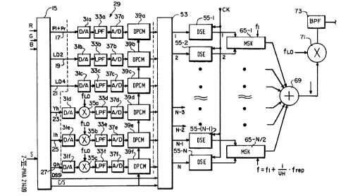
Turning back now to Eigure 2, six data streams
with varying bit rates and mutually exclusive time inter-
vals, with the exception of the data streams representative
of the LD2 and the LD4 data from HDTV encoder 15 are
coupled from the bit rate reducer 29 to a multiplexer/
buffer memory 53. After a suitable delay of either the LD2
or LD4 data stream to provide a totality of mutually
exclusive time intervals the data bit streams are sequent-
ially stored in the memory of the multiplexer/buffer
memory 53 wherein they are divided into N data streams
of equal length and equal bit rate which are respectively
and simultaneously coupled to N direct sequence encoders
(DSE) 55-1 to 55-N.
A modulo-2 addition is performed on the low
bit-rate streams by the DSE to provide a code sequence
at a predetermined increased bit rate for each of the data
streams emanating from the multiplexer/buffer memory 53.
A circuit for accomplishing this bit rate conversion is
shown in Figure 4a. A pseudo-noise sequence generator 57
(PNSG) having a sequence rating at the desired conversion
bit rate is coupled to one terminal of an exclusive OR
gate 59, the other terminal of which is coupled to receive
the data stream. Exclusive OR gate 59 provides an encoded
.
P~-~.21409 7 13210~-4
data stream at a bit rate determined by the bit rate of
the pseudo noise sequence generator 59. Only a small
percentage of the possible codes that may be generated
by the PNSG are utilized to achieve a code repetition
rate equal to the TV frame repetition rate. Each code has
a defined start point synchronized to the TV frame start.
Of all the possible codes available from the PNSG 57 only
N codes are choses and their start points are defined
such that each source bit to be transmitted is represented
by a unique sequence within the repetition time of the code
sequences. For a 200K bit/sec data rate, as in a preferred
embodiment of the invention, a 6M bit/sec rate for the
sequencing bits may, for example, be adopted thus
establishing an appreciable overhead to allow for an
optimum selection of sequences.
Extracting the initial data stream from the
encoded data stream may be accomplished with the same
circuitry, this time acting as a direct sequence decoder
(DSD), as shown in Figure 4b. In this figure a PNSG 61
is coupled to one input terminal of an exclusive OR gate 63,
the other terminal of which is coupled to receive the
encoded data stream. PNSG 61 is in synchronism with the
encoded data stream thereby providing the original data
stream at the output terminal of exclusive OR gate 63.
Turning back again to Figure 2, to provide
minimum sidelobes for the transmitted signals the N coded
data streams at the PNSG bit rate are combined in pairs
and provided at an intermediate frequency (IF) spectrum
by minimum shi~t key (MSK) modulators 65-1 through 65-N/2.
These MSK modulators provide a sequence of pulses at the
intermediate frequency which constitute the coded signals.
These signals are not infinite sequences, existing only
for a small fraction of a frame time. Signals of this
type exhibit spectral lobes within a .sin(x)/x envelope
determined by the width of the pulses in the sequence.
Such a spectrum is represented in Figures 5a and 5b. If the
width of the pulses within the sequence is equal to T,
the nulls of the sin(x)/x are at frequencies spaced from
PHA.2140~ 8 1321014
the center frequency equal to the reciprocal of the pulse
width. Spectral lobes within the envelope have frequency
spacing that are equal to the repetition rate of the pulses
of the sequence, as shown in Figure 5b, which is an expanded
view of the area 67 in Figure 5a. The width of these lobes
is a function of the number of pulses in the sequence
and the repetition rate and is equal to twice the repetition
rate divided by the number of pulses plus one. Though not
shown in the Figure each spectral lobe has a number of
side lobes associated therewith.
Each MSK modulator uses a different modulation
carrier frequency. If the initial frequency is equal to K
times the repetition frequency and each succeeding frequency
is displaced from this initial frequency by i/(N+1) f(rep)
is should be apparent that when i equals N the gap between
two spectral lobes will be filled as illustrated in Figure
5c. A summation network 69 is coupled to the output termi-
nals of the MSK modulators to receive modulated signals and
provide the summation thereof to a mixer 71 wherein they
are converted and coupled via a bandpass filter 73 for
transmission.
The combination of direct sequence encoding and
minimum shift key modulation establishes a noise like
spectral distribution for the radiated signal, spreading
the signal energy over a relatively wide band of frequencies.
Th$~ spread spectrum radiation has a very low power spectral
density which would be deep in the noise of analog detectors
operating in a finite band. Consequently these signals
may radiate in the VHF and UHF taboo bands and not interfere
with analog transmissions in these bands.
Referring to Figure 6 the transmitted signal is
received and heterodyned in mixer 75 operating at a local
o~cillator (L0) frequency and passed through band pass
filter 77 to a bank of MSK demodulators 79-1 through
79-N/2. Each of these demodulators operates at a demodula-
tion carrier frequency corresponding to a modulation
carrier frequency used in the transmitter. As a result,
N nearly identical baseband spectrum are generated.
PHA.21409 9 1321014
Each baseband signal is coupled to an associated comb
filter in a bank of comb filters 81-1 through 81-N to
suppress unwanted and unnecessary spectral components
and improve interchannel isolation. These filtered signals
are then coupled to N direct sequence decoders (DSD) 83-1
through 83-N to restore the original equal length equal
bit rate data streams. A clock signal for the different
DS decoders is provided by input 82, and synchronization
for this decoding is provided on synchronisation signal
10 connection 85 from the main channel TV signal.
Each equal length, equal bit rate data stream is coupled
to a demultiplexer/buffer memory ~7 wherein the demulti-
plexing operation reestablishes the original six DPCM
encoded signals. Decoding of the DPCM encoded signals is
15 accomplished in decoders 89a through 89f as previously
described with reference to Figure 3b. Reestablishment
of the high definition TV coded signals continues with the
digital to analog (D/A) conversion of the decoded DPCM
signals in digital to analog converters 91a through 91f.
20 The enhancement signals~ in analog form, corresponding
to LD2, LD4, and the left and right panel enhancement
signals are coupled through low pass filters 93a-93c,
converted to digital signals in analog to digital conver-ters
(A/D) 95a - 95c whereat the left and right panel encoded
25 signals have been reestablished. The LD2 and LD4 are
further processed by time compressing these digital signals
by 4:3 in compressors 97a-97b.
The analog luminance and chrominance signals are
frequency shifted in mixers 99a - 99c~ bandpass filtered
30 in filters 101a - 101c, converted to digital signals in
analog to digital (A/D) converters 95d - 95f wherefrom
reestablished encoded luminance and chrominance signals
are provided.
Finally, all signals are coupled to a HDTV
35 decoder 103 which provides RGB signals suitable for display
on a display device (not shown).
132101~
PHA.2140~ lO
While the invention has been described in its
preferred embodirnents it is to be understood that the words
whi.ch have been used are words of description rather than
of limitation and the changes within the purview of the
appended clairns may be made without departure from the
true scope and spirit of the invention in its broader
aspects.