Note: Descriptions are shown in the official language in which they were submitted.
~ ~ 2 ~
1 TITLE OF THE INVENTION
Process for Producing Compound Semiconductor
and Semiconductor Device Using Compound Semiconductor
Obtained by Same
BAC~GROUND OF THE INVENTION
.
Field of the Invention
This invention relates to a process for
producing a compound semiconductor having a desired
10 conduction type region and a semiconductor device
obtained by using the same.
Related Background Art
In the prior art, for formation of pn junction
in compound semiconductors, the liquid phase growth
15 method, the MOCVD method, the MBE method have been
practiced. Among them, the liquid pha~e growth method
has been primarily practiced, and therefore
description thereof is set forth below by referring to
an example.
~O Liquid phase growth utilizes slow-cooled
epita~ial growth, namely difference in the conduction
type layers deposited due to difference in
temperature.
Fig. :18A shows the carrier concent~ation
25 distribution near the pn junction of a compound
semiconductor formed by the above prior art method.
- . :. . .
,,
- 2 - ~32
1 Fig. 18B shows the change in carrier concentration
corresponding to the relationship between solution
temperature and time. Initially, when the solution
temperature is T1, the region n~ear the substrate is a
5 conductive layer having a high carrier concentration
of n-type, and n-type carrier concentration is reduced
as the temperature is lowered. And, at the point of
the temperature of T2, the n-p reversal temperature is
reached and pn junction is formed. When slow cooling
10 is further continued, p-type layer will grow while
becoming higher concentration, until growth i~
completed at the temperature T3 by departing the
substrate from the solution.
~hen growth is performed by use of this
15 method, as is apparent from Fig. 18A, the carrier
concentration near the pn junction becomes lower,
whereby there is the problem that when a device is
formed, its response speed becomes delayed.
Also, although it is possible to grow
20 similarly a compound semiconductor crystal by the
MOGVD method or the MB~ method as previously -
mentioned, the above methods have not yet been
technically establi~hed, and cannot be said to be
sufficiently reliable.
Further, since the cryQtal growth by use of
the three kinds of methods as mentioned above is
- 3 ~
1 epitaxial growth, there is the drawback that an
expensive compound semiconductor substrate such as
GaAs, etc. must be used as the substrate.
Besides, as to the structures of grown layers,
5 in all of the prior art examples, the pn junction
faces will become in parallel to the substrate
surface.
SUMMARY OF THE INYENTION
The present invention has been accomplished in
view of the above points, and its primary object is to
provide a process for producing a compound
semiconductor which has solved the problems as
described above of the prior art.
Another object of the present invention is to
provide a process for producing a novel compound
semiconductor which can produce a compound
semiconductor easily and with good reproducibility and
bulk productivity.
Still another ob~ect of the present invention
is to provide a process for producing a compound
semiconductor which can provide a compound
semiconductor capable of forming a semiconductor
electronic device improved in respon~e speed with good
25 reliability.
Yet another object of the present invention is
.
.
. . . . -
:
- 4 - 132~2~
1 to provide a process for producing a compound
semiconductor, which comprises applying a crystal
forming treatment on a substrate having a free surface
comprising a nonnucleation surface (SNDs) with a
5 smaller nucleation density and a nucleation surface
(SNDL) arranged adjacent thereto having a sufficiently
small area for a crystal to grow only from a single
nucleus and a larger nucleation density (NDL) than the
nucleation density (NDS) of said nonnucleation surface
10 (SNDS), by exposing the substrate to either of the gas
phases:
(a) gas phase (a) containing a starting material
(II) for feeding the group II atoms of the periodic
table and a starting material (VI) for feeding the
15 group VI atoms of the periodic table and
(b) gas phase (b) containing a starting material
(III) for feeding the group III atoms of the periodic
table and a starting material (V) for feeding the
group V atoms of the periodic table, thereby forming
~0 only a single nucleus on said nucleation surface
~SNDL) and permitting a monocrystal of the compound
semiconductor to grow from said single nucleus,
characterized in that a semiconductor junction is
formed in said monocrystal by feeding a starting
25 material (Dn) for feeding a dopant for controlling to
one electroco:nduction type and a starting material
`t ~
t,
, ~ '
, : -, ;''~,, '
~ : '
132~121
1 (Dp) for feeding a dopant for controlling to the
electroconduction type opposite to said electro-
conduction type with change-ove:r to one another into
said gas phase, during said crystal forming treatment.
Yet still another object of the present
invention is to provide a process for producing a
compound semiconductor, which comprises applying a
crystal forming treatment on a ~ubstrate having a free
surface comprising a nonnucleation surface (SNDS) with
10 a smaller nucleation density and a nucleation surface
(SNDL) arranged adjacent thereto having a sufficiently
small area for a crystal to grow only from a single
nucleus and a larger nucleation density (NDL) than the
nucleation density (ND5~ of said nonnucleation surface
15 (SNDs), by exposing the substrate to either of the gas
phases:
(a) gas phase (a) containing a starting material
(II) for feeding the group II atoms of the periodic
table and a starting material (VI) for feeding the
20 group VI atoms of the periodic table and
(b) gas phase ~b) containing a starting material
(III) for feeding the group III atoms of the periodic
table and a starting material (V) for feeding the
group V atoms of the periodic table, thereby forming
25 only a single nucleus on said nucleation surface
(SNDL) and permitting a monocrystal of the compound
" ~ 1 `i " '
: . .. ., . ~ .:
- 6 - ~ 3~
1 semiconductor to grow from said single nucleus,
characterized in that a semiconductor junction is
formed in said monocrystal by feeding a starting
material (Dn) for feeding a dopant for controlling to
5 one electroconduction type while changing the
introduced amount of said starting material (Dn) with
the lapse of time.
Again another object of the present invention
is to provide a semiconductor device by use of the
10 compound semiconductor obtained by the above
production process.
BRI~F DESCRIPTION OF THE DRAWIN~S
Fig. 1 illustrates the relationship between
15 the size of the nucleus rc and the free energy G.
Figs. 2A and 2B illustrate schematically the
selective deposition method.
Figs. 3A - 3D illustrate diagramatically the
steps of a first example of the formation process for
20 crystals according to the present invention.
Figs. 4A and 4B are perspective views in Figs.
3A and 3D.
Figs. 5A - 5D are diagrams of the formation
steps of the crystal showing a second example of the
25 crystal forming process of the present invention.
Figs. 6A - 6D are diagrams of the formation
~.
:" , : , ,
'' ~'' ~ :"`
_ 7 - ~32~S~
1 steps showing a third example of the process for
forming the crystal of the present invention.
Figs. 7A and 7B are perspective views of Figs.
6A and 6D.
Figs. 8A - 8E are diagrams of the formation
steps of the crystal showing a first embodiment of the
present invention.
Fig. 9 illustrates the pnp junction transistor
using a monocrystal obtained in accordance with the
10 present invention.
Figs. lOA and lOB illustrate another junction
type semiconductor device using a monocrystal obtained
in accordance with the present invention.
Figs. llA-llC and 12A-12E are diagrams of the
15 steps of a second embodiment of the present invention.
Fi~. 13 illustrates the substrate for crystal
formation used in the present invention.
Figs. 14A and 14B illustrate another
semiconductor device using a monocrystal obtained in
20 accordance with the present invention.
Figs. 15A-15J are diagrams-of the formation
steps of the LED device in one example of the present
invention.
Figs. 16A-16I are diagrams of the formation
25 steps of the L~D device in another example of the
present invention.
~i~
,.. . . :
:
- 8 - ~32112
1 Fig. 17 illustrates the X-Y matrix two-
dimensional planer LED device using a monocrystal
obtained by the present invention.
Fig. 18A shows the carrier concentration
5 distribution near the pn junction of a compound
semiconductor formed by the above prior art method and
Fig. 18B shows the change in carrier concentration
correspondlng to the relationship between solution
temperature and time.
DLSCRIPTION OF THE PR~FERRED ~MBODIMLNTS
In the present invention, a desired conduction
type region is formed by changing the growth
conditions during crystal growth of a compound
15 semiconductor on the nucleation surface (SNDL) by
utilizing nucleation density difference (~ND).
First, for better understanding of the present
invention, as the related basic technology, general
thin film forming process of a metal or a
20 semiconductor is to be explained.
When the deposition surface (crystal growth
s~rface) is of a material different in kind from the
flying atoms, particularly an amorphous material, the
flying atoms will be freely diffu~ed on the ~ubstrate
25 surface and reevaporated (eliminated). And, as the
result of col.Lision mutually between the atoms, a
,y ~
.
- 9 - 132~21
1 nucleus is formed, and when the nucleus reaches the
size rc (=-2~0/gv) or more at which its free energy G
becomes the maximum (critical nucleus~, G is reduced
and the nucleus continues to grow stably three-
S dimensionally and become shaped in an island. Thenucleus with a si-~e exceeding rc is called "stable
nucleus" and in the basic description of the present
invention hereinbelow, "nucleus" unless otherwise
specifically noted indicates the "stable nucleus".
Also, of the "stable nucl~us", one with small
r is called "initial nucleus". The free energy G
formed by formation of the nucleus is represented by:
G=4æf(~)(~0r2 + 1~3-gv-r3)
f(~)=1/4(2 - 3 cos~ + cos2~)
5 where r: radius of curvature of nucleus
~: contact angle of nucleus
gv: free energy per unit volume
: surface energy between nucelus and
vacuum.
20 The manner in which G is changed is shown in Fig. l.
In the same Figure, the curvature of-radius of the
stable nucleus when G is at the maximum value is rc.
Thus, the nucleus grows to become shaped in an
island, and further grows until contact mutually
25 between islan~s proceeds, giving rise to coalescence
in some cases, finally forming via a network structure
1321~ 21
1 a continuous film to cover completely the substrate
surface. Through such process, a thin film is
deposited on the substrate.
In the deposition process as described above,
5 the density of the nucleus formed per unit area of the
substrate surface, the size of the nucleus and the
nucleation speed are determined depending on the state
of the system of deposition, and particularly the
interaction between the flying atoms and the substrate
10 surface substance is an important factor. Also, a
specific crystal direction grows in parallel to the
substrate depending on the anisotropy relative to the
crystal face of the interfacial energy at the
interface between the deposited substance and the
15 substrate, and when the substrate is amorphous, the
crystal directions within the substrate plane are not
constant. For this reason, a grain boundary is formed
by collision mutually between nuclei or islands.
Particularly, in case of collisio~ mutually between
20 islands with certain sizes or greater, coalescence
will occur, leading directly to formation of a grain
boundary. The grain boundary formed can be migrated
with difficulty in the solid phase, and therefore the
grain size is determined at that point.
Next, the selective deposition film forming
method for fcrming selectively a deposited film on the
~`
-:,~ :,' ,. , ' "`, ~; ,
1 3 2 ~
1 deposition surface is to be described. The selective
deposition film forming method is a method in which a
thin film is selectively formed on the substrate by
utilizing the difference between the materials in the
5 factors influencing nucleation in the thin film
forming process such as surface energy, attachment
coefficient, elimination coefficient, surface
diffusion speed, etc.
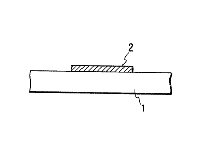
Figs. 2A and 2B illustrate schematically the
10 selective deposition film forming method. First, as
shown in Fig. 2A, on the substrate 1, a thin film 2
comprising a material different in the abo~e factors
from the substrate 1 is formed at a desired portion on
the substrate 1. And, when deposition of a thin film
15 comprising an appropriate material is performed
according to appropriate deposition conditions, it
becomes possible to cause a phenomenon to occur such
that the thin film 3 will grow only on the free
surface of the thin film 2 without growth on the free
20 surface of the substrate 1. By utilizing this
phenomenon, the thin film 3 self-alignmently formed
can be permitted to grow, whereby the lithographic
step by use of a resist as practiced in the prior art
can be omitted.
As the materials which can be deposited by
such selective deposition film forming method, there
, K.
. ~ ' ' '`'~ ' .
! ~. ~ , , .
. .,
' ' ' , ' . " ' "', ' ' . '
- 12 -
:l 3 2 ~
1 may be included, for example, SiO2 as the substrate 1,
Si, GaAs, silicon nitride as the thin film 2, and Si,
W, GaAs, InP, etc. as the thin film 3 to be deposited.
The II - VI group compound crystal can be
5 grown on a Si substrate, or a II - VI group compound
substrate, and cannot be grown on SiO2 substrate as is
known in the art. However, by implanting ions of the
group III elements (atoms), the group V elements
~atoms), or ions of the group II elements (atoms), the
10 group VI elements (atoms) of the periodic table on a
SiO2 substrate, the nucleation density (ND) at the ion
implanted portion can be enhanced to make the
difference (~ND) in nucleation density from the SiO2
substrate sufficiently large, whereby selective
15 deposition of the group II - VI compound can be
effected.
The III - V group compound crystal can be
grown on a Si substrate, a III - V group compound
substrate, and cannot be grown on SiO2 substrate as is
20 known in the art. However, by implanting ions of the
group III elements (atoms), the group V elements
(atoms), or ions of the group II elements (atoms), the
group VI elements (atoms) of the periodic table on a
SiO2 substrate, the nucleation density (N~) at the ion
25 implanted portion can be enhanced to make the
difference (~ND) in nucleation density from SiO2
- ~. . . . .
: -.. - ...... ,, :~:
- 13 - 132~
1 substrate sufficiently large, whereby selective
deposition of the group III - V compound can be
effected.
Also, it is possible to add a different
5 material having larger nucleation density (NDL) to the
material surface having smaller nucleation density
~NDS) such as SiO2 substrate and form selectively a
deposited film by utilizing the nucleation density
difference (~ND).
The present invention utilizes the selective
deposition method based on such nucleation density
difference (~ND), and a nucleation surface comprising
a material which has sufficiently larger nucleation
density than the material forming the deposition
15 surface (crystal formation surface) and is different
from ~he latter material is formed sufficiently finely
so that only a ~ingle nucleus may grow, whereby a
single crystal is grown selectively only from such a
fine nucleation surface.
Since the selective growth of single crystal
is determined depending on the electron state of the
nucleation surface, particularly the state of dangling
bond, the material with lower nucleation density for
forming the nucleation surface (e.g. SiO2) is not
25 required to be a bulk material, but the nucleation
surface may be formed on the surface of any desired
: :, . :
3 2 ~
1 material substrate.
Next, the outline of the process for forming
crystals according to the present invention is
described in detail by referrin~ to the drawings.
Figs. 3A - 3D illustrate diagramatically the
steps of a first example of the formation process for
cry~tals according to the present invention, and Figs.
4A and 4B are perspectlve views in Figs. 3A and 3D.
First, as shown in Fig. 3A and Fig. 4A, on the
10 substrate 4 comprising high melting point glass,
quartz, alumina, ceramics, etc., a thin film 5 with
small nucleation density enabling selective nucleation
tnonnucleation surface (SNDS)] is formed, and a
material different from the material forming the thin
15 film 6 with small nucleation density is thinly
deposited thereon, followed by patterning by
lithography, etc. to form sufficiently finely a
nucleation surface comprising a different material
(SNDL) (or called "Seed") 6, thus obtain~ng a
20 substrate for crystal formation. However, the size,
the crystal structure and the composition of the
substrate 4 may be as desir~d, and it may be also a
substrate having a functional device previously formed
thereon by the conventional semiconductor technique.
25 Al~o, the nucl.eation surface (SNDL) 6 comprising a
different mate!rial is, as described above, inclusive
. .
.
- ' `~ ' : ' ' ~ ~ ',
. . . :
- 15 - ~ ~2~
1 of Se, As modified regions formed by ion implantation
on the thin film 5 The nucleation surface in the
surface on which substantially only single nucleus is
formed and is constituted of an amorphous material.
Next, by selecting appropriate deposition
conditions, a monocrystal of a thin film material is
formed only on the nucleation surface (SNDL) 6. That
is, the nucleation surface (SNDL) 6 is required to be
formed sufficiently finely to the extent that only a
10 single nucleus may be formed. The size of the
nucleation surface (SNDL) 6, which depends on the kind
of the material, may be several microns or less.
Further, the nucleus grows while maintaining a single
crystal structure to become a single crystal grain 7
15 shaped in an island a~ shown in Fig. 3B. For the
island-shaped single crystal grain 7 to be formed, it
is desirable to determine the conditions for crystal
forming treatment cO that no nucleation may occur at
all on the free surface of the thin film 5.
The island-shaped monocrystalline grain 7
further grows while maintaining the monocrystalline
structure with the nucleation surface (SNDL) 6 as the
center (lateral overgrowth~, whereby the thin film 5
can be partially or wholly covered therewith as shown
25 in Fig. 3C (monocrystal 7A).
Subsequently, the surface of the monocrystal
- . ~. . . : ..... ; - : .: - -:. .: :
.: - .. .: . . .
- 36 - ~2~2~
1 Fig. 15D:
In a PC13 atmosphere, heat treatment was
performed at ~00 C for 10 minutes, and then a p-type
semiconductor monocrystalline island 1504 of SaP was
5 grown by use of the MOCVD method. As the starting
materials, trimethylgallium (TMG) and PH3 were
employed. PH3 was decomposed by the hot cracking
method immediately before introduction and fed into
the reaction tube. The molar ratio of TMG to PH3 was
lO 2:1 and the diluting gas was H2. The reaction
pressure was normal, and the substr~te temperature was
850 C.
In the starting material for feeding the
p-type dopant, 0.02% of diethylzinc (DEZn) was mixed.
15 Fig. 15E and Fig. 15F:
When the p-type GaP 1504 grew to a desired
size, the doping gas was changed from DEZn to selenium
hydride (H2Se~ to grow n-type GaP 1505. H2Se was
mixed TO 0.05~.
20 Fig. 15G:
The upper portion of the monocrystalline
islands 1504, 1506 were flattened by mechanical
polishing.
Fig. 15H:
A~ter preparation of a negative pattern with a
resist, Au-Ni (20:1~ was vapor deposited to 3000 A.
' "' ' '- : " ' , '
~': ,. .: ,,,, .. : ' :: `'
-: :` - ' ' ' ., ~
-.. : .. , :- , -, , .
.. ` ,~. . . .
.-.- . ,............. .
- 17 - 1~21, ~1
1 a substrate 9 comprising a material with a smaller
nucleation density (ND) enabling selective nucleation,
to provide a substrate for crystal formation and a
monocrystalline layer 8 can be formed on said
5 substrate similarly as in the ~irst example.
Figs. 6A - 6D are digra~ms of the formation
steps showing a third example of the process for
forming the crystal according to the present
invention, and Figs. 7A and 7B are perspective views
10 of Figs. 6A and 6D.
As shown in Fig. 6A and Fig. ~A, on an
amorphous insulating material substrate 11, nucleation
surfaces (SNDL) 12-1, 12-2 are arranged sufficiently
small with a material different from the above
15 substrate 11 with a distance n therebetween. The
distance Q may be set equal to the size of the single
crystal region required for formation of, for example,
a semiconductor device or a group of devices or
greater than that.
Next, by selecting appropriate crystal forming
conditions, only one nucleus of the crystal forming
material is formed on only the nucleation surfaces
(SNDL) 12-1, 12-2. That is, the nucleation surfaces
(SNDL) 12-1, l2-2 are required to be formed to
25 sufficiently fine sizes (area-c~) to the extent that
only a single nucleus may be formed. The sizes of the
,. :.: ..:.
`. : :
,~ .
. ~ ; :.
- 18 - 1 ~2
1 nucleation surfaces (SNDL) 12-:l, 12-2, which may
differ depending on the Xind oi' the material, may be
preferably 10 ~m or less, more preferably 5 ~m or
less, optimally 1 ~m or less. Further, the nucleus
5 grows while maintaining a monocrystalline structure to
become island-shaped single crystal grains 13-1, 13-2
as shown in Fig. 6~. For islancl-shaped monocrystal
grains 13-1, 13-2 to be formed, as already mentioned,
it is desirable to determine the conditions for
10 crystal forming treatment so that no nucleation will
occur at all on other surfaces than the nucleation
surfaces (SNDL~ on the substrate 11.
The crystal orientations of the island-shaped
single crystal grains 13-1, 13-2 in the normal
1~ direction of the substrate 11 are constantly
determined such that the interface energy of the
material is made minimum. For, the surface or the
interface energy has anisotropy depending on the
crystal face. However, as already mentioned, the
20 crystal orientation within the substrate plane in an
amorphous substrate cannot be determined.
The island-shaped monocrystalline grains 13-1,
13-2 further grow to become monocrystals 13A-1, 13A-2,
whereby adjolning monocrystals 13A-1 13A-2 contact
25 mutualy each other as shown in Fig. 6C, but since the
crystal orientation within the substrate plane i~ not
" ~, .
- .
:
:, :
. . .
- lg -
1 3 2 ~
1 constant, a crystal grain boundary 14 is formed in the
middle portion between the nucleation surfaces (SNDL)
12-1 and 12-2.
Subse~uently, single crystals 13A-1, 13A-2
5 grow three-dimensionally, but the crystal face with
slower growth speed will appear as the facet. For
this reason, flattening of the surfaces of
monocrystals 13A-1, 13-2 is performed by etching or
polishing, and further the portion of the grain
lO boundary 14 is removed, to form the thin films 15-1,
15-2, 15 of single crystals containing no grain
boundary in shape of lattice as shown in Fig. 6D and
Fig. 7B. The sizes of the monocrystalline thin films
15-1, 15-2, 15 are determined by the distance Q
15 between the nucleation surfaces (SNDL) 12 as described
above. That i5, by defining appropriately the
formation pattern of the nucleation surfaces (SNDL)
12, the position of the grain boundary can be
controlled to form monocrystals with desired sizes at
20 a desired arrangement.
The present invention utilizes the crystal
formation process as described above by referring to
Fig. 3A to Fig. ~B by way of example.
In the present invention, in the above crystal
25 formation process, crystal forming treatment is
performed in ~as phase, and either one of:
,:: ~ ~ .' : ,`' " `' '~' .. ' '
- 20 -
~ 3 2 ~
1 (a) gas phase (a) containing a starting material
(II) for feeding the group II atoms of the periodic
table and a starting material ~VI) for feeding the
group VI atoms of the periodic table and
(b) gas phase (b) containing a starting material
(III~ for feeding the group III atoms of the periodic
table and a starting material (V) for feeding the
group V atoms of the periodic tabl~, is selected as
the gas phase, and a semiconductor junction is formed
10 in the crystal of the compound semiconductor formed by
feeding into the selected gas phase a starting
material (~) for feeding a dopant to control the
conduction type as mertioned in the semiconductor
field thereof with change-over of their kind
15 corresponding to the kind of conduction type.
The typical crystal of the compound
semiconductor obtained in the process for producing
the compound semiconductor of the present invention is
the so-called II - VI group compound ~emiconductor
20 crystal and the III - V group compound semiconductor
crystal.
As the respective starting materials to be
used in the production process of the present
invention, there may be included specifically the
25 following compounds as suitable examples.
As the starting material (II) for feeding the
:,
:
- 21 -
~ 3 2 ~
1 group II atoms of the periodic table (abbreviated as
"the group II atoms"), for necessity to be Ped into
gas phase, those which are under gaseous state or
readily gasifiable are preferred.
These points can be said to be applicable
similarly to the starting material (VI) for feeding
the group VI atoms of the periodic table (abbreviated
a~ "the group VI atoms"), the starting material (III)
for feeding the group III atoms of the periodic table
10 (abbreviated as "the group III atoms"), the starting
material (V) for feeding the group V atoms of the
periodic table (abbreviated as "the group V atoms")
and the starting material (D) for feeding dopant.
As the starting material (II), there may be
15 included dimethyl zinc, diethyl zinc (Zn(C2H5)2),
dimethyl cadmium (Cd(CH3)2), diethyl cadmium, dipropyl
cadmium (Cd~C3H7)2~, dibutyl cadmium ~Cd(C4Hg)2),
dimethyl mercury ~Hg(CH3)2), diethyl mercury
~Hg~C2H5)2), etc., and as the starting material lVI)
20 hydrogen sulfide (H2S), selenium hydride, dimethyl
-~elenium, diethyl selenium (Se(C2H5)2), dimethyl
diselenide ~CH3SeCH3), dimethyl tellurium (Te(CH3)2),
diethyl tellurium (Te(C2H5)~), etc. By combination of
these starting materials (II) and (VI), monocrystals
25 of II - VI group compound semiconductors such as ZnS,
ZnTe, CdS, CdTe, HgSe, ZnO, etc. and mixed crystal
... . .
... :. . .
- 22 -
~321~21
1 compound monocrystals of these can be selectively
formed on the nucleation surface ~SNDL).
In the case of obtaining III - V group
compound semiconductor crystals, by use of trimethyl
5 indium In(CH3)3 as the starting material (III) and
phosphine PH3 as the starting material (V), InP
monocrystals can be formed selectively on an amorphous
substrate, and also AlSb monocrystals by use of
trimethyl aluminum Al(CH3)3 as the starting material
10 (III) and stibine SbH3 as the starting material ~V).
By combination of the respective starting materials as
described above, monocrystals of either one of GaP,
GaSb, InAs, InSb, AlAs and AlP can be selectively
grown, and further any desired combination of mixed
15 crystal III - V group compound monocrystals can be
selectively ~rown.
As the starting materials (III), the above
compounds having methyl group are not limitative, but
it is also possible to use compounds having ethyl
20 group, propyl group, butyl group, isobutyl group such
as triethyl ~allium Ga(C2H5)3, tripropyl indium
In(C3H~)3, tributyl gallium Ga(C4Hg)3, triisobutyl
aluminum Al(CH3)2CHC~2, etc.
First embodiment
Figs. 8A - 8~ illustrate a first embodiment of
the present invention.
.
- 23 -
1321~1
1 First, a nonnucleation surface 802 is formed
on a substrate 801. Next, a nucleation surface 803 is
formed sufficiently finely so that a single nucleus
may be formed. This size may be preferably 10 ~m or
5 less, more preferably 5 ~m or lless, as described
above. Optimally it is 1 ~um or less. The materials
for forming such nonnucleation surface 802 and
nucleation surface 803 may differ depending on the
crystalline material constituting the monocrystals to
lO be formed. In the case of forming monocrystals of
GaAs, an amorphous material such as silicon nitride,
aluminum oxide ,etc. may be used a~ the material for
forming the nucleation surface 803, and silicon oxide,
etc. may be used as the material for forming the
15 nonnucleation surface 802. Also, as shown in Fig. 8A,
without formation of a fil~ on the substrate 801, for
example, As ions may be implanted into the SiO2 film
in an excessive amount, and the modified region thus
formed may be used as the nucleation surface 803. In
20 the case of producing a II - VI group compound
semiconductor such as ZnS, ZnSe, CdSe, etc., silicon
oxide, etc. may be u~ed as the material for forming
the nonnucleation surface 802, while as the material
for forming the nucleation surface 803, an amorphous
25 material such as silicon nitride, aluminum oxide, etc.
may be employed. Also, similarly as in the case of
,,. ~
- 24 -
~32~
1 III - V group, without formation of a film, Se ions
may be implanted into the SiO2 film in an excessive
amount, and the modified region thus formed may be
used as the nucleation surface 803.
Fig. 8A shows a substrate having a
nonnucleation surface 802 with smaller nucleation
density thus formed, and a nucleation surface 803
which is arranged ad~acent to said nonnucleation
surface 802, has an area sufficiently small for a
10 crystal to grow only from a single nucleus 804 and has
a nucleation density greater than said nonnucleation
surface 802.
In the present invention, by applying a
crystal forming treatment to the substrate, a single
15 nucleus 804 is formed and a monocrystal is permitted
to grow from said single nucleus. At the stage of
forming said single nucleus 804, there is no problem
whether the dopant may be added or not. The crystal
forming treatment of the present invention has the
20 step of crystal formation in which a starting material
(Dn) for feeding a dopant for controlling to one
conduction type is added to the gas phase for crystal
forming treatment and the step of crystal ~ormation in
which the starting material (Dp) for Peeding a dopant
25 for controlling to the opposite conduction type is
added to the above gas pha~e.
.
: :.
,
- 25 - 1~2~J~
1 For example, in practicing the present
invention for formation of crystals of III - V group
compound semiconductor, for controlling the conduction
type to p-type, the atoms of the group II of the
5 periodic table such as Zn, Be, etc. can be used.
For controlling the conduction type to n-type,
the atoms of the group IV of the periodic table such
as Si, Ge, Sn, etc. or the atoms of the group VI of
the periodic table such as S, Se, Te, etc. can be used
10 as the n-type dopant.
In the case of practicing the present
invention for formation of crystals of a II - VI group
compound semiconductor, for controlling the conduction
type to the p-type, the atoms of the group V of the
15 periodic table such as P, N, As, etc. can be used as
the p-type dopant, while for controlling to the n-
type, the atoms of the group III of the periodic table
such as B, Al, Ga, etc., or the atoms of the group VII
of the periodic table such as F, Cl, etc. can be used
20 as the n-type dopant. These dopants can be
incorporated into the crystals by feeding the starting
material (D) for feeding dopant into the gas phase for
carrying out crystal forming treatment during the
crystal forming treatmentO
~5 In the present invention, by feeding the
starting material (Dn) for feeding the n~type dopant
; . . ~
"
- 26 - ~32~121
1 and the starting material (Dp) for feeding the p-type
dopant into the gas phase containing the starting
materials for feeding the atoms which become the
matrix of the crystals to be fo;rmed, namely, the above
5 starting materials (II~ and (VI~ in the case of II -
VI group compound semiconductor, with switchover to
one another, a semico~ductor junction is formed in the
crystals formed.
The starting materials (D) similarly as in the
lO case of the starting materials (II), (VI), (III) and
(V), may be suitably selected from among those which
are gaseous or readily gasifiable and will not give
bad influence to the crystals formed.
Specifically, the starting material (Dn) may
15 include, for the II - VI group compound semiconductor,
B2H6, AlR3, GaR3, InR3, HF, Hcl and the like; for III -
V group compound semiconductor, H2S, SR2, H2Se, SeR2,
TeR2, SiH4, GeH4, SnR4 and the like as suitable ones.
The starting material (Dp) may include, for II - VI
20 group compound semiconductor, PH3, NH3, AsH3, RAsH3
and the like; for III - V group compound
semiconductor, ZnR2, BeR2 and the like as suitable
ones. In those formulas, R represent~ an alkyl group,
prefera~ly CH3 or C2H5.
As shown in Fig. 8B, after a single nucleus
803 is formed on the nucleation surface 803, or during
,.:
:
,
'' ; . : ,~
~211,~1
1 formation of the single nucleus, by adding a desired
amount of the starting material (D) for feeding the
dopant for controlling the conduction type in addition
to the starting material (M~ for feeding the atoms
5 which become the matrix of the crystals formed into
the gas phase for crystal forming treatment, a
monocrystalline semiconductor region 805 with a
desired conduction type can be formed.
For example, when a starting material (Dp~ for
10 feeding the p-type dopant is employed as the starting
material (D) for feeding the dopant, the semiconductor
region 8Q6 becomes the p-type semiconductor region,
while if the starting material (Dn~ for feeding the n-
type dopant is employed, the semiconductor region 805
1~ becomes the n-type semiconductor region. In the
figure, the semiconductor region 805 is shown as the p-
type. At the ~tage, when the semiconductor region 805
has grown to a desired size, by switching the starting
material ~D) for feeding the dopant to the starting
20 material for feeding the dopant of the conduction type
~ different from the conduction type of the
semiconductor region 805, a semiconductor region 806
different in the conduction type from the
semiconductor region 805 can be formed continuously
25 around the semiconductor region 805.
For example, when the semiconductor region 805
.. ..
: ', - :.,, -
`' 1''' ~ ~ '` `. ~'
; .
-
- 28 - i ~2 ~ 21
1 is the p-type, by adding a desired amount of the
starting material (Dn) for feeding the n-type dopant
into the gas phase for crystal forming treatment, the
conduction type of the semiconductor region 807 can be
5 made the n-~ype. Thus, by switching over the kind of
the starting material (D) for feeding dopant at
appropriate times as desired, a semiconductor junction
can be formed in the monocrystal of the compound
semiconductor formed. Fig. 8D shows the state in
10 which pn junction is formed, and Fig. 8E shows the
state in which pnp junction is formed.
As shown in Fig. 8E, by flattening by removing
the upper portion of the monocrystal of the compound
semiconductor having pnp junction formed, a
15 semiconductor monocrystalline region having the pnp
junction in the plane direction of the su~strate 801
can be made on the substrate 801 as shown in Fig. 9.
By providing electrodes 901, 902 and 903 on the upper
surfaces of the p-type region 805a, the n-type region
20 806a and the p-type region 80~a of the semiconductor
monocrystalline region thus formed, respectively, a
pnp type transistor can be obtained.
Second ~mbodiment
Similarly as in the case of the first
25 embodiment, after a compound semiconductor monocrystal
having pnp ~unction is formed as shown in Fig. 8~, the
.
.
~ ' L
- 29 - 132~ hl
1 upper end portion of the monocrystal is removed to be
flattened similarly as in the case shown in Fig. 9
(Fig. lOA).
Then, by providing electrically separating
5 regions 1005, 1006 in the vertical direction on the
main surface of the substrate 1001, a semiconductor
region having pnpnp junction and a semiconductor
region having pnp junction are formed. Its upper
plane view is shown in Fig. lOB. As shown in Fig.
10 lOB, the semiconductor region having pnpn junction is
constituted of the p-type semiconductor region 1004a,
the n-type semiconductor region 1003a, the p-type
semiconductor region 1002a, the n-type semiconductor
region 1003b and the p-type semiconductor region
15 1004b. The semiconductor region having pnp junction
is constituted o~ the p-type semiconductor region
1002b, the n-type semiconductor region 1003c, the p-
type semiconductor region 1004c.
By providing electrodes respectively on the
20 upper plane surfaces of the semiconductor regions
- electrically separated similarly as in the case of
Fig. 9, the semiconductor device having pnpnp junction
and the semiconductor device having pnp junction can
be formed at the same time on the sub~trate 1001.
As the method for electrical separation, there
may be employed the method for cutting spacially by
- : ~
, -
,~
132~2~
1 etching, etc. or the method in which a predetermined
semiconductor region is made higher in resistance by
ion implantation, etc. In the case when the compound
semiconductor monocrystal is GaAs, as the ions to be
5 implanted, Cr ions can be implanted to form partially
a region with increased resistance.
The present invention is described in detail
by referring to Examples.
10 Example 1
Figs. llA - llC and Figs. 12A - 12E are
diagrams showing the preparation steps of L~D with GAP
compound monocrystalline semiconductor.
First, according to Figs. llA - llC, a
15 substrate for growing a compound monocrystalline
semiconductor crystal was formed.
Fig. llA:
On the surface of the glass substrate 1101,
SiO2 layer 1102 of about 1000 A was formed by the
20 normal pressure CVD method by use of SiH4 and 2
Fig. llB:
A photoresist layer 1103 was applied and
patterning was effected slo as to make a window portion
1104 of 2 ~m s.quare ~generally it may be some ~m
25 square or less~). And, by use of an ion implanter, P3
ions were implanted in an amount of 1 x 10¹⁶/cm2 onto
- 31 - 1 32~ 12 ~
1 SiO2 layer 1102 (this portion becomes the nucleation
surface with high nucleation density and is
hereinafter called seed portion).
Fig. llC:
After the photoresist .Layer 1103 was peeled
off, the substrate 1101 surface was subjected to heat
treatment in PCl3 atmosphere at 1050 C for 10
minutes, to obtain a substrate for GaP selective
nucleus growth such that the region 1105 implanted
10 with P3 exists at a certain portion on SiO2 layer
1102.
Figs. 12A - 12E are diagrams of steps for
forming a planar type LED device region by growing
continuously GaP monocrystal from p-type to n-type on
15 the above substrate. The respective steps are as
described below.
Fig. 12A:
On the substrate obtained in Fig. llC, a
monocrystalline nucleus 1106 of GaP was formed by u~e
20 of the MOCVD method. As the starting materials,
~ trimethylgallium (TMG) and PH3 were employed. PH3 was
decomposed by the hot cracking method immediately
before introduction and fed into the reaction tube.
The TMG/PH3 molar ratio was 1.5 and the diluting gas
25 was H2. At this time, in order to make p-type, 0.02%
of (C2H5)2Zn was mixed.
-. , ~
.
;
- 32 -
132112 i
1 Fig. 12B:
The above monocrystalline nucleus was
homoepitaxially grown to form a p-type GaP
semiconductor region 1106.
5 Fig. 12C:
When p-type GaP monocrystalline region 1106
grew to a certain size, the doping gas was switched to
H2Se (O.05~), to grow a n-type GaP semiconductor
region 1107.
10 Fig. 12D:
When a GaP semiconductor monocrystalline
island with a double layer structure of p-type and n-
type was prepared, as shown in Fig. 12D mechanical
polishing was performed in parallel to the substrate
15 so that the p-type semiconductor region 1106 was
exposed to effect flattening of the upper portion of
the monocrystal. On the right side of Fig. 12D there
is shown the state as viewed from above the substrate.
Fig. 12B:
On the flattened GaP monocrystal, electrodes
were attached to form a LED device. As the electrode
1108 of the p-type region 1106, an alloy of Ag-In-Zn
(8:1:1) was used, which was vapor deposited and
subjected to heat treatment at 650 C in Ar atmo~phere
25 for 5 minutes. On the other hand, as the electrode
1109 of the n--type region 110~, an alloy of ~u-Ni
~` `
?~.
- 33 -
132 Llh l
1 (20:1) was used, which was vapor deposited and
subjected to heat treatment at 550 C in H2 atmosphere
for 2 minutes.
The LED device of GaP thus obtained exhibited
5 a light emission spectrum having a peak near 560 nm,
similarly as the GaP prepared by use of a
monocrystalline wafer.
Example 2
In this example, the seed portion
10 ~corresponding to 1105 in Fig. llC) was formed by thin
film patterning. In Example 1, the seed portion 1105
was obtained by implanting P3 ions into the fine
portion in the crystal growth region, but in this
example, the seed portion 1303 was obtained by
15 depositing an Al203 thin film and further subjecting
the Al203 film to fine patterning. The details are
as described below.
(a) Similarly as in Example 1, an SiO~ layer
1302 was deposited on a glass substrate 1301.
~b) Next, by use of the ion plating method, an
~ Al203 film was deposited to about 300 A. That is, by
means of an arc discharge type ion plating device,
after evacuation to 10 5 Torr, 2 ga~ was introduced
to 1 x 10 4 - 3 x 10 4 Torr, and an Al203 film was
25 deposited under the conditions of an ionization
voltage 50V (output 500W), a substrate potential of -
'~'i'~,
-; . :
.~:
.: :
- 34 -
132~
1 50 V, and a substrate temperature of 400C.
(c) As shown in Fig. 13, the Al203 film was
subjected to patterning to 2 ~m by use of the
photolithographic technique to form the seed portion
5 1303- The etchant was H3po4:HNo3:cH3cooH H20=16 1 2 1
(40 C)
(d) After the photoresist was peeled off, an
LED of GaP was prepared by employing the same steps as
in Example 1. The LED device obtained exhibited light
10 emission having a peak at around 560 nm similarly as
in Example 1.
~xample 3
In this example, GaAs was grown. Also for
GaAs, TMG and AsH3 were used as the starting gases,
15 and p-type and n-type could be freely controlled by
use of Si as the n-type dopant and Be as the p-type
dopant similarly as in growth of GaP.
Example 4
In this example, a MES type FET as shown in
20 Figs. 14A, 14B was formed. In the MES type FET shown
in Fig. 14A, a three-layer structure was formed in the
order of n , n, n+ and electrodes were attached as
shown in Fig.14A after mechanical flattening. In the
MES type FET shown in Fig. 14B, a double layer
25 structure was formed in the order of n+, n and, after
mechanical flattening, the n+ region was separated
..: . :.. ~
: -:
: ., .
.
_ 35 - 1~2~
1 into two insulated parts, followed by attachment of
the electrodes as shown in Fig. 14B. In Figs. 14A,
14B, G represents Schottky gate electrode, S source
electrode and D drain electrode. The compound
5 semiconductor monocrystal used was GaP.
Example 5
Figs. 15A - Fig. 15J are preparation steps
showing an example of GaP light emission diode.
10 Fig. 15A:
On the surface of the substrate 1501, SiO2
layer 1502 of about 1000 A thickness was deposited by
the CVD method by use of SiH4 and 2 The sputtering
method may be used in place of the CVD method.
15 Fig. 15B:
Patterning was effected with a photoresist
film provided on the SiO2 layer 1502, followed by
masking with the window portion of 1 ~m2 being
remained. And, by use of an ion implanter, P3 ions
20 were implanted in an amount of 1 x 10¹⁶/cm2 into the
SiO2 layer 1502.
Fig. 15C:
At t~e portion of the SiO2 layer 1502
corresponding to the window portion of the
25 photoresist, a seed portion 1503 implanted with P ions
was formed.
, . ? I
., .
,
,
- 36 - ~ ~2 1 ~ 21
1 Fig. 15D:
In a PCl3 atmosphere, l1eat treatment was
performed at 900 C for 10 mimltes, and then a p-type
semiconductor monocrystalline island 1504 of 5aP was
5 grown by use of the MOCVD methc)d. As the starting
materials, trimethylgallium (TMG) and PH3 were
employed. PH3 was decomposed by the hot cracking
method immediately before introduction and fed into
the reaction tube. The molar ratio of TMG to PH3 was
10 2:1 and the diluting gas was H2. The reaction
pressure was normal, and the substrate temperature was
850 C.
In the starting material for feeding the
p-type dopant, 0.02% of diethylzinc (DE2n) was mixed.
15 Fig. 15E and Fig. 15F:
When the p-type GaP 1504 grew to a desired
size, the doping gas was changed from DEZn to selenium
h~dride (H2Se) to grow n-type GaP 1505. ~2Se was
mixed TO 0.05%.
20 Fig. 15G:
The upper portion of the monocrystalline
islands 1504, 1506 were flattened by mechanical
polishing.
Fig. 15H:
After preparation of a negative pattern with a
resist, Au-Ni (20:1) was vapor deposited to 3000 A.
,,.~,
- 3~ ~ 1 32~ :~. 21
1 The resist was dissolved by use of a solvent to lift
off unnecessary portions, thereby forming an n-side
electrode 1506. Further, the electrode was heated in
H2 atmosphere at 550 C for 2 ~inutes.
5 Fig. 15I:
An SiO2 film 1507 was deposited to 4000 A by
the sputtering method, and a contact hole 1508 to the
n-layer was formed by use of the photolithographic
technique.
lO Fig. 15J:
Ag-In-Zn (8:1:1) was deposited to 6000 A by
vapor deposition, subjected to patterning with a
photoresist and then a p-side electrode 1509 was
formed according to the dry etching method by use of
15 CCl2F2. Further, the electrode was heated in Ar
atmosphere at 650 C for 5 minutes. Thus, a LED
device was prepared.
When a transparent material such as SiO2 is
used as the substrate 1501, light emissicn occurs from
20 the bottom of the device through the substrate 1501.
~ On the contrary, when the substrate 1501 is opaque as
alumina, by making the electrodes 1506, 1509 except
for the contact portions transparent electrodes such
as of ITO, li~ht emission can be effected from the
25 direction before of the substrate 1501 (upper part in
the drawing).
:,.
,
- 3~ -
1~21 ~
1 ~xample 6
Figs. 16A - Fig. 16I are diagrams of the steps
for preparation of a GaN light emission diode which is
one of MIS type LED. The respective steps are
5 described below.
Fig. 16A:
An SiO2 film 1602 was cleposited to about 1000
A on the surface of the substrate 1601 according to
the CVD method by use of SiH4 and 2
10 Fig. 16B:
Next, by use of the ion plating method, an
Al203 film was deposited to 300 A. That is, by means
of an arc discharge type ion plating device, after
evacuation to 10 5 Torr, 2 gas was introduced to 1 -
15 3 x 10 4 Torr, and A1203 was deposited under theconditions of an ionization voltage 50V (output 500W),
a substrate potential of -50 V, and a substrate
temperature of 400 C. Then, resist patterning, and
followed by patterning to 1.5 ~m with an etchant
~0 ~H3P04:HN03:CH3COOH:H20=16 l 2 1~ 40 C) were
- effected, thereby forming a seed portion 1603 of
Al203.
Fig. 16C:
In PCl3 atmosphere, heat treatment was
25 conducted at 950 C for 10 minutes, and then a
monocrystalline island 1604 of n-type GaN was grown by
.
'
., . :. -. . . .
', :'
:.,
, ',' ' ~,
~3~112~
1 the MOCVD method. As the starting gases,
trimethylgallium ~TMG) and ammc)nia (NH3) were
employed, with the TMG/NH3 molar ratio being made 120,
and the diluting gas H2. The reaction pressure was
5 made normal, and the substrate temperature 1000 C.
Fig. 16D:
The grown monocrystalline island 1604 of GaN
was flattened by mechanical polishing.
Fig. 16E and Fig. 16F:
After patterning with a photoresist 1605, Zn
ions 1606 were implanted in an amount of 1 x 10¹⁶/cm2,
and heated in H2 atmosphere at 900 C for 5 minutes to
form an insulating layer 1607 (high resistance GaN
layer).
15 Fig. 16G:
After preparation of a negative pattern with a
resist, In-Al was vapor deposited to 2000 A . Next,
the resist was dissolved to lift off unnecessary
portions, thereby forming an electrode 1608.
20 Fig. 16H:
- SiO2 was deposited to 3000 A by the sputtering
method, and a contact hole 1610 to the insulating
layer 1607 was formed by use of the photolithographic
technique.
25 Fig. 16I:
In-Al was vapor deposited to 5000 A, followed
- 40 -
lL 3 ~ h ~L
1 by patterning to form an electrode 1611 on the
insulating layer 160~ side. As the etchant,
FeCl3:HCl:H20=2:3:10 was employed. When the MIS type
LED of GaN,thus prepared was subjected to light
5 emission actuation, good emission characteristics were
exhibited.
The selective nucleation LED preparation steps
of GaP, GaN as described above can be practiced not
only by the above MOCVD method, but also by the MBE
10 method and the LP~ method. Also, they are applicable
also for other compound semiconductor materials other
than GaP and GaN.
Fig. 17 is a plane view of a LED array
comprising a plural number of the p-n junction type
15 LED as previously explained as ~xample 5 arranged on a
single substrate. 1701 shown in this Figure is a n-
type GaP crystal, 1~02 a p-type GaP crystal, 1703 and
1704 are electrodes (see Figs. 15G - Fig. 15J).
Also, it is possible to form an LED array by
20 use of the MIS type LED explained as Example 6 other
than the p-n junction type LED.
Further, by arranging LLD's having a plural
number of emission colors within the LED array, for
example, by arranging L~D's of R, G and B emission, a
25 color image displayer can be also constituted. Here,
it is suitable to u~e GaA~P as the R ~red color)
. :~
t ' "
':'~" ' "
`: ' , ' , -
- 41 ~ 1 3 2 ~
1 emitting LED, GaP as the G ~green color) emitting LED
and GaN as the B (blue color) emitting LED.
As described above, according to the present
invention, enlargement of area and low cost of the
5 substrate can be realized by the technique for
building up selectively a compound semiconductor
crystal in shape of islands at any desired position of
any desired substrate. Also, the pn junction face
obtained by practicing the present invention is
10 exposed as positioned in the direction approximately
vertical to the substrate surface, and therefore the
steps of device formation can be simplified by
reducing the number of photopatterning during device
formation.
The effects of the present invention may be
more specifically enumerated as follows.
1) Because of selective nucleus growth on any
desired substrate, the substrate is not limited to
expensive compound semiconductor substrates.
2) Because a crystal can be grown only on the
desired position, it is possible-to completely effect
insulating separation mutually between the devices
during formation of devices.
3) Since the pn junction face obtained by
~5 practicing the present invention is not in parallel to
the substrate but exposed in the direction vertical
'
~32~
1 thereto, the photoetching steps, etc. during device
formation can be omitted to a great extent.
As another effect, a LED device can be easily
prepared on any desired base substrate at any desired
5 position.
By doing so, a large scale display device
which is hither to prepared by hibridization of a
large number of LED devices can be easily prepared as
the monolithic constituton.
Alsol it becomes possible to prepare a one-
dimensional light source or two-dimensional (plane
emission) light source by a LED array with monolithic
constitution.
Further, according to the present invention,
15 since it becomes also possible to form LED on a
substrate such as ceramics, etc., reduction of
production cost can be effected.