Note: Descriptions are shown in the official language in which they were submitted.
132~2~3
CASE 3016
-- 1 --
HIGH PERFORMANCE ANGLED
STRIPE SUPERLUMINESCENT DIODE
The invention relates to an improved
superluminescent diode and in particular, to an angled
stripe superluminescent diode having improved lateral
confin~ment.
BACKGROUND 0~ THE INVENTION
High power radiation emitting devices, such
as semiconductor lasers, typically comprise a body of
semiconductor material having opposed end faces in
which an active layer is positioned between two
cladding regions of opposite conductivity. Gain, which
is necessary for these high power devices, results from
a population inversion which occurs when applied
current is increased. The end faces of the body form a
resonant cavity such that radiation
generated in the active layer is partially raflected
back into the semiconductor body by an end face toward
the opposing end face. When the current is
sufficiently increased above some threshold value the
increase in gain causes lasing action to occur.
Lasers emit a narrow band of highly coherent radiation
~'
;~, '` ~.i ' ~, `, ' , ' ' ' ''
-- ~32~2~ Case 301~
-- 2 --
having a coherence length of approximately 2
centimeters (cm). Coherent radiation, or radiation
having narrow line width, is undesirable in some
applications, such as fiber optic gyroscopes, which
require high power devices which emit radiation having
low coherence. Other devices such as light emitting
diodes (LED's) emit a broad band of radiation but
operate at low power, insufficient for high power
applications.
Superluminescent diodes (SLDs) provide a
high power output of hroad band low coherent
radiation, that being radiation having a coherence
length of less than about 200 micrometers (~m) and
typically about 50 ~m. An SLD typically has a
structure similar to that of a laser, with lasing
being prevented ~y antireflection coatings formed on
the end faces. These coatings must reduce the
reflectivity of the end faces to about 10-5 or less
to prevent lasing in a high power SLD and further,
this reflectivity must be reduced to about 10-6 to
achieve low spectral modulation. Spectral modulation
is the percentage ratio of the difference between the
maximum and minimum power output divided by the sum of
the maximum and minimum power output a~d low spectral
modulation is 5% or less modulation. Unfortunately,
low reflectivity of about 10-6 at the end faces is
difficult to obtain consistently for a given output
wavelength and even a slight temperature change which
alters the output wavelength will change the
reflectivity, thus making the manufacture of l~w
spectral modulation SLDs extremely difficult.
Other SLD structures utilize a stripe
interrupt geometry in which a metallized stripe is
formed over a portion of an active region. This
stripe extends from one end face towards but not up to
,~ , ;
¦ ~2 ~ Case 3016
the opposing end face. The non-metallized region is
supposed to be highly absorbing to greatly reduce
reflection from the facet near that region. However
the high optical field is known to bleach this
absorbing region, maXing it somewhat transparent to
the light propagating through it. As a result, facet
reflection is not ~ufficiently eliminated, and the
device exhibits high spectral modulation or evan
becomes a laser at high power.
Due to the aforementioned problems, an SLD
has been limited to a maximum output power of about 7
mw continuous wave (cw) and has had high spectral
modulation.
In U.S. patent 4,821,227 issued
April 11, 1989 in the names of Alphonse
and Gilbert, there is disclosed an angled stripe SLD
where a gain guiding stripe is tilted with respect to
the normal to the cleaved facet resulting in low
reflectance in the optical beam path. For best
results the angle of the tilt with respect to the
normal has been less than 5~. The efficiency of this
SLD is limited by its lack of lateral confinement at
the active region Por the optical beam path. While it
is known that higher efficiency devices can be
obtained by using index-guided structures, this would
result in some reflected rays being trapped in the
optical beam pa~h. To reduce the trapping of
reflected rays the stripe angle would have to be
larger than 5-~ However, a stripe angle larger than
this angle is not practical because the corr sponding
hiqh refraction angle in ~ir would make fiber coupling
to the SLD difPicult.
SUMMARy OF THE INVENTION
It is therefore an object of the present
invention to provide a super luminescent device having
''
'~
,
-
.: .: ' : -~` '
.
~ ~2 ~ Case 3016
-- 4 --
improved lateral confin~ment of the optical beam path
which does not result in an increase of reflection
back along the optical beam path.
It is another object of the present
invention to provide a super luminescent device having
improve.d lateral confinement of the optical beam path
without having to increase the angle of reflection at
the end face of the device which would hamper fiber
coupling.
In accordance with a broad aspect of the
present invention ~here is provided a super
luminescent light emitting device comprising a
semiconductor body having spaced first and second
opposed end faces with an active region extending
therebetween. The body includes a central region and
two opposing end regions extending a predetermined
distance from the end faces to the central region.
The device has gain guiding means comprising a linear
strip of material adjacent to a side of the active
region extending between the end faces and inclined
along its longitudinal axis at a predetermined angle
relative to a direction normal to at least one of the
end faces. The device includes an optical beam path
extending between the end faces in the active region
parallel to the longitudinal axis of the gain guiding
means. The optical beam path has end lateral
boundaries at each of the ~nd regions whose lateral
carrier and optical confinement is determined by the
gain guiding means to allow light reflected at the end
faces to be refracted out of the optical beam path.
The de~ice further includes an index guiding means
extending over ~he central region on opposite sides of
the gain guiding means parallel to the longitudinal
axis o~ the gain guiding means. The index guiding
means determines
-- ~ 3 2 ~ Case 3016
-- 5 --
central lateral boundaries for the optical beam path
to provide lateral carrier and optical confinement of
the optical beam path in the central region.
The super luminescent device of the present
invention allows for improvements in the efficiency in
the operation of the super luminescent device because
of an improvement in lateral confinement of the
optical beam path in the central region. However, the
improved lateral confinement does not extend over the
end regions o~ the device which allows for reflected
rays to be refracted out of the optical path while not
ha~ing to increase the angle of the longitudinal axis
of the gain guiding means incident to the normal to
the end face. An improved operating efficiency is
obtained without increases in spectral modulation and
increases of refraction angle in air permitting for
practical fiber coupling.
In accordance with another aspect of khe
present invention the lateral step in the index of
refraction in the end regions of the optical path is
less than the lateral step in the index of refraction
in the central region of the optical path.
In accordance with one embodiment of the
present invention the index guided means comprises an
index guided ridge waveguide. It is envisaged that
the index guided ridge may comprise a ridge extending
solely along the central region of the body of the
device defined by two troughs located on either side
of the strip. It is further envisaged that the index
ridge waveguide may include two troughs located on
either side of the st,rip where the troughs extend
parallel to the longitudinal axis of the strip over
the central region and extend laterally outwardly of
the strip in the end regions.
In accordance with another embodimenk of the
~ , : ( : . , , :
2~ Case 3016
-- 6 --
present invention the device may comprise a buried
heterostructure device with the index guided means
comprising a regrown region at the central region that
provides a positive index guide over the central
region.
BRIEF DESCRIPTION OF THE DRAWINGS
For a better understanding of the nature and
objects of the present invention reference may be had
by way of example to the accompanying diagrammatic
drawings in which:
Figure 1 is a perspective view of a
preferred embodiment of a super luminescent device of
the present invention;
Figure 2 is a sectional view of the device
of Figure 1 at section lines II-II;
Figure 3 is a sectional view of the device
of Figure 1 at section lines III-III;
Figure 4 is a top view of an optical path
for the device shown in Figure 1;
Figure 5 is a perspective view of another
embodiment of a a super luminescent device of the
present invention; and
Figure 6 is a perspective view of a buried
heterostructure super luminescent device in
accordance with another embodiment of the present
invention.
DETAILED DESCRIPTION_OF THE PREFERRED EMBODIMENTS
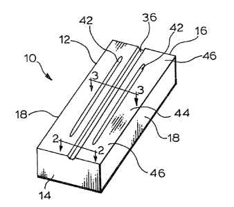
Referring to Figures 1 and 2, a super
luminescent light-emitting device 10 comprises a body
12 having first and -econd opposed end faces 14 and
16, respectively, and sidewalls 18 extending
therebetween. The body 12 at the end faces 14 and 16
includes a substrate 20 having a first cladding layer
22 thereon, an active layer 24 overlying the first
cladding layer 20, a second cladding layer 26
- 13~2~ Case 3016
- 7
overlying the active layer 24, an etch stop layer 28
overlying the second cladding layer, a third cladding
layer 30 overlying the etch stop layer 28, and a
capping layer 32 overlying the third cladding layer
30. An electrically insulating layer 34, having an
aperture 36 therethrough which extends between the end
faces 14 and 16, respectively, and which is
nonperpendicular relative to the first and second end
faces 14 and 16, respectively, overlies the capping
layer 32. A means for electrically contacting the
body 12 comprises a first electrical contact 38 which
overlies the surface of the substrate 20 opposite the
firsk cladding layer 22 and a second electrical
contact 40 which overlies the capping layer 32 in the
aperture 36 and insulating layer 34.
The substrate 20 and first cladding layer 22
are of one conductivity t~pe and the second cladding
layer 26, etch stop layer 28, third cladding layer 30
and capping layer 32 are of the opposite conductivity
type. The refractive index of the active layer 24
should be greater than the refractive index of both
the first and second cladding layers 22 and 26,
respectively. The body is typically composed of
binary group III-V compounds such as GaAs and alloys
of such compounds.
The substrate 20 is typically composed of
N-type GaAs about 100 microme~ers ~m) thick and has a
first major surface ~arall~l to or slightly
misoriented from the (100) crystallographic plane.
The first cladding layer ~2 typically combines the
functions of a buffer layer and a cladding laye~. The
first cladding layer 22 is about 1.5 ~m thick. The
second cladding layer 26 is about 0.12 ~m thick. The
third cladding layer 30 is about 1.6 ~m thick. The
cladding layers 22, 26 and 30 are typically composed
13212~ Case 3016
-- 8
of AlxGal_xAs where x is generally between about
0.4 and 0.5 and typically about 0.45. The active
layer 24 is typically about 0.07 ~m thick and is
generally composed of ~1xGal_xA~ where x is
between about 0 and 0.1, depending on the wavelength
to be emitted. The etch stop layer 28 is typically
about 0.03 ~m thick and is composed of AlxGal_xAs
where x is typically about 0.1. The capping layer 32
is typically about 0.45 ~m thick and is typically
composed of P-type GaAs. The insulating layer 34 is
typically about 0.15 ~m thick and is preferably
composed of silicon oxide deposited by pyrolytic
decomposition of a silicon-containing gas, such as
silane, in oxygen or water vapor.
The aperture 36, which is non-perpendicular
relative to at least one end face and typically both
end faces, provides a means for defining an effective
optical beam path by gain guiding within the device.
Typically the yain guiding means is a current
confining structure, such as the second electrical
contact 40 in the aperture 36, which is in the shape
of a linear stripe about 5 to 7 ~m wide in the lateral
direction, that being the direction perpendicular to
the planes of the sidewalls 18. Thie current confining
structure extends between the pair of opposed parallel
end faces, 14 and 16 respectively, and has an axis of
symmetry which is at an angle e relative to the
direction perpendicular to the end faces as shown in
Figure 4. The tangent of the angle e must be greater
than or equal to the effective width of the optical
beam path in the device divided by the length of the
body between the first and second end faces 14 and 16,
respectively. ~his minimizes the Fabry-Perot
reflections which oc-_ur in a laser cavity due to
reflections occurring between the end faces 14 and 16
"'
~ 13~2~ case 301~
_ g _
respectively.
Referring to Figures 1 and 3, the super
luminescent ligh~ emitting devices is illustrated to
include two troughs or wells 42. The troughs 42 are
formed through standard photolithographic, chemical
etching and the depth of the troughs 42 is determined
by etch stop layer 28. The troughs 42 provide a ridge
over the central region 44 of the device which acts as
an index guiding means. The index guiding means for
index-guided ridge 48 in this preferred embodiment has
edges 50 on opposing sides of the gain guiding strip
36 extending parallel to the longitudinal axis of the
gain guiding strip. For strips 36 in the order of 3
~m to 5 ~min width the ridge at the central region in
the order of 5 to 7 ~m in width, respectively. The
index guided ridge determines the central lateral
boundaries of the optical beam path providing lateral
carrier and optical confinement of the optical beam
path in the central region 44.
The index guiding means or ridge 48 has the
edges 50 extending in the parallel relation to the
strip longitudinal axis to within a predetermined
distance from the end faces 14 and 16 of the device
12. Over this predetermined distance, the lateral
width of the optical path and optical confinement are
determined solely by the gain guiding strip 36. This
predetermined distance is referred to as the end
regions 46 of device 10. The device 10 has a lenyth
of 300 ~m with end regions of 25 ~m leaving a central
region of 250 ~m. The width of the wells are in the
order of 10 to 12 ~m.
Referring to Figure 3, the angle e must have
a value such that 2e exceeds the critical value for
lateral reflection, that being the angle at which
there is no refracted ray and thereby total internal
.. -~ . ............................ . .
-,
~ 2 ~ 2 ~ ~ Case 3016
-- 10
reflection exists. For example, the optical beam path
has differences in its effective refractive index
between that portion of the gain region 23 under the
ridge and the remaining laterally adjacent portion of
the gain region. These differences in effective
refractive index are determined over the central
region 44 by the index guiding ridge 48 and over the
end regions 46 by the gain guiding strip 36. This
difference in index of refraction along the central
region 42 of the optical path is greater than the
difference of effective index of refraction of the
optical beam path over the end regions 44. The
difference in effective index of refraction over the
central region is about 0.02 and serves to confine
radiation within the optical beam path of the device
enhancing operatin~ ~fficiency. The difference of
effective index of refraction of the optical path over
the end regions is less than 0.005 and permits
reflections in the optical beam path at the end faces
14 and 16 to be re~racted out of the optical beam path
resulting in low spectral modulation. To achieve this
in the end region 46, the angle 2e must be greater
than the critical angle. The critical angle ~c is
determined as follows:
~c = Sin~l [l-(n2/nl)2]~
where nl is the effective refractive index of the
gain region 23 containing the optical b~am and is
typically about 3.35 and n2 is the effective
refractive index o~ the laterally adjacent region and
is typically about 3.345. Therefore, ec i~
typically about 3.13 and the angle e must be greater
than 1.6 and is chosen to about 5 to account for
dif~raction spread. The angle ~ may be about equal to
: .
~3~12~3 Case 3G16
the Brewster angle which is equal to the inverse
tangent of the refractive index of the medium adjacent
the first end face 14, divided by the transverse
effective refractive index for light propagating
between the end faces. The medium adjacent the first
end face 14 is typically air having a refractive inde~
of about 1 and the refractive index of the body 10 is
typically 3.35 for GaAs devices. Thus, the Brewster
angle is typically about 16.6. At the Brewster angle
the radiation vibrating in the plane of incidence is
not reflected, thus resulting in radiation which is
predominantly polarized. Further, at this angle the
reflected and refracted rays are 90 apart resulting
in a non-reflective condition at the emitting end
face. This condition allows the elimination of
antireflection coatings on the devices' end faces
which are typically used to increase output.
The body 10 may be fabricated using
liquid-phase epitaxy techniques to deposit the
layers. Suitable liquid-phase epitaxy techniques have
been disclosed by Nelson in U.S. Patent No. 3,565,702,
issued February 23, 1971 and Lockwood et al in U.S.
Patent No. 3,753,801, issued August 21, 1973. Other
epitaxial growth includes vapor phase, organometallic
vapor phase, and molecular beam epitaxy. The aperture
36 is formed in the silicon oxide insulating layer 34
by first forming a photoresist layer having an angled
stripe aper~ure therein, over the insulating layer 34
which is then etched by a suitable etchant such as
buffered hydrofluoric acid.
The first electrical contact 38 is
preferably composed of sequentially deposited
germanium, gold, nickel, and gold layers. The second
electrical contact 40 is preferably composed of
titanium, platinum and gold layers which are
.: , ::: ,:
-, , , : , :.
-
- ~ ,
: ~ . , :- , , ,
- 1321~ Case 3016
- 12 -
sequentially deposited onto a zinc or cadmium diffused
surface.
It should be understood that improved
current confinement can be obtained by having the
capping layer 3~ composed of N-type GaAs with zinc
diffused therethrough in the region of aperture 36.
This will permit for better definition of the lateral
boundaries of the optical beam path as defined by the
gain guiding means over the end regions 46.
In the operation of the device 10 a bias
voltage of the proper polarity is applied to the
electrical contacts 38 and 40 respectively, producing
light emission in the active region. The aperture 36
provides a means for reducing on-axis reflections of
light between the end faces resulting in an emission
having low coherence. This device described having
index guiding has demonstrated 1% spectral modulation
at an output power of 20 mw, cw and a slope efficiency
of 0.18 mw/mA.
It should be understood that the present
invention may be implemented using any suitable index
guiding means or structure that effectively controls
the current and optical lateral confinement of the
optical beam through the central region of the
device. This may include other ridge guide structures
such as the embodiment shown in Figure 5, for
example. In this embodiment, the width of the ridges
is different at the end regions 46 than over the
central region 44. Index guiding may be implemented
by buried heterostructure devices such as shown in
Figure 6, for example, or buried ridge devices.
,, -, ~: . ,: . .............. ...... -;, : . ,
', ' ..... ~ ': " , , '` '
- , , , ' ' , ~