Note: Descriptions are shown in the official language in which they were submitted.
~3212~
AIR VELOCITY TRANSMITTER DEVICE
This invention relates to an air velocity trans-
mitter, and more particularly, to a device for accurately
measuring the velocity of an air flow and providing a linear
signal that may be employed to control the operation of commer-
cial and industrial energy management systems, or being employed
wherever measurement and control of air or other gas flow
is needed.
Wrobel and Ashton U.S. Patent No. 4,537,068, granted
August 27 r 1985 (assigned to the same assignor as the instant
application), discloses a thermal anemometer arranged to
measure air velocity in which the anemometer comprises a
probe containing two separate and distinct sensing elements,
and a hand held electronic readout unit that contains sensing
signal electronic processing circuitry, function control,
and an analog readout meter, with the probe and readout unit
being interconnected by a self coiling cable. The probe
sensing elements are a self heated thermistor and a solid
state temperature sensing device, and are separately but
simultaneously exposed, in the u~e of the instrument, to
the air flow to be measured, with the energy consumed by
the thermistor and its resulting signal, being an indication
of both the velocity of the air stream and the difference
in temperature between the forced operating temperature of
the thermistor and the air stream ambient temperature. The
solid state temperature sensing device is a temperature sensing
transistor, and develops a signal that is proportional to
the air stream temperature. The two signals ~re electronically
combined at the readout unit to eliminate the effect of any
ambient temperature variations, to provide an air stream
~ 32~ 26~
velocity reading at the meter that is independent of ambient
temperature.
Devices for measuring air flow and velocity find
many uses. However, control of air flow, as distinguished
from measuring of same, has proved to be difficult to achieve
in this art due to the tendency of sign~ls being generated
by thermistors mounted for probe use to generate non-linear
signals and the effect of temperature differentials between ~ -
the operating temperature of the thermistor and the ambient
temperature of the air stream being measured.
While the unit of this invention has its major
utility in connection with air flow, the unit involved is
also fully applicable to any gas flow; consequently, the
term "air" as used in this disclosure and claims means both
air and other gases, separately or mixed.
A principal object of the present invention is
to provide an air velocity transmitter device that not only
accurately measures air velocity in either high or low rates
of air flow, but also provides a signal that is linear with
respect to air velocity that is available, in the use of
the device, for lnstance, control, digitized sensing readout,
and/or record keeping purposes.
Another principal object of the invention is to
provide an air velocity transmitter device in which a plurality
of separate air velocity ranges are available by merely changing
the positions of "off-on" switches, with the need for poten-
tiometer adjustment in the field being eliminated.
Yet another principal object of the invention is
to provide an air velocity transmitter having an output signal
that is independent of temperature variations in the measured
air flow.
1 3 2 ~
Still another principal object of the invention
is to provide an air velocity transmitter device that may
be powered by either direct current or alternating current
electrical energy from any convenient external source.
In accordance with the invention, an air velocity
transmitter device is provided comprising an anemometer type
probe that is employed to measure the air flow, and a housing
containing electronic circuitry to which the probe is elec-
trically connected for providing a unit that, when powered
by either an alternating current (AC) or direct current (DC~
power supplyr furnishes, when the probe is utilized, a signal
in the industry preferred 4-20 milliamp range that is linear
with respect to velocity of the air flow, for remote or local
control and/or readout of air velocity.
The unit is powered by electrical connection to
any convenient external source of electrical power, that
may be either AC or DC in the range of from about 22 to about
28 volts. The probe is applied to one end of the unit cable,
the other end of which is electrically connected to the elec-
tronic processing and readout circuitry of the unit housing.
The probe mounts two separate and distinct sensing elements ;
for exposure to the air stream to be measured and controlled.
One of the probe sensing elements is the velocity sensor
and is similar to the thermistor of said Wrobel and Ashton
patent, it being arranged to be operated in a self heated
mode as the velocity sensing element of the unit, and is
incorporated in one branch of a self regulating bridge circuit,
with the bridge circuit being arranged to force the thermistor
to operate at a particular resistance that corresponds to
a specific temperature, at 200 C. in the disclosed embodiment.
~32~2~
Air movement across the thermistor will cause an increase
in the input power required to maintain the indicated operating
temperature of the thermistor with the energy being consumed
by the thermistor being an indication of both the velocity
of the air stream and the difference in temperature between
the operating temperature of the thermistor and the ambient
temperature of the air stream.
The other sensing element of the probe is in the
form of a chip thermistor that forms the opposite arm of
the said self regulating bridge circuit, the thermistor chip
being located in the probe to sense the temperature of the
air flow but it is operated in a mode that is not effected
by velocity of the air flow involved. As ambient temperature
changes, the chip thermistor increases or decreases its resis-
tance such that the voltage across the velocity sensor is
not affected by ambient temperature variations,
The resulting non-linear signal is applied to signal
processing circuitry within the unit housing that adjusts
same for gain and offset, with the thus adjusted signal being
applied to a linearizer circuit that is also within the unit
housing, to provide a signal that is linear with respect
to air velocity and supplies the 4-20 milliamp signal for
the unit, with the linealizer circuit also being arranged
to provide multiple velocity ranges by merely changing the
position of "off-on" switches.
Other objects, uses, and advantages will be obvious
or become apparent from a consideration of the following
detailed description and the application drawings in which
like reference numerals indicate like parts throughout the
several views.
1~2~2~
In the drawings:
Figure 1 is an exploded perspective view diagram-
matically illustrating an air velocity transmitter unit ar-
ranged in accordance with the present invention, with the
external electrical power sources being omitted from this
view (to simplify the drawing), and with the cable of the
unit being shown broken away as the cable can be any desired
length, depending on whether the unit housing and associated
parts are located adjacent to or removed from the air flow
that is to be measured by the transmitter of Figure l;
Figure 2 is similar to Figure 1, but shows only
the transmitter circuit board and the linearizer circuit
board of the uni' of Figure 1, in the same relation as shown
in Figure 1, but on a larger scale;
Figure 3 is a view of the probe of the unit of --
Figure 1, shown on an enlarged scale and largely in section
to better illustrate the probe circuit board and sensor devices
as well as the probe porting therefor, and showing also the
probe end cover in place when the transmitter unit is not
in use;
Figure 4 is a highly simplified representation
of the instrument probe sensors and the basic electrical
energy sourcing and signal processing circuits that the probe
components are electrically associated with;
Figure 5 is a flow sheet type illustration indicating
the different stages of processing of the probe signal that
is received from the unit txansmitter board to provide the
output signal of the unit;
Figures 6 - 14 diagrammatically and schematically
illustrate the several circuits or subcircuits that are in-
~32~26~
volved in the unit circuitry, with the individual Figuresillustrating the following circuits:
Figure 6 illustrates the power source and voltage
regulator circuit;
Figure 7 illustrates the thermistor control circuit;
Figure 8 illustrates the probe output adjustment
circuit;
Figure 9 illustrates the analog to digital input
circuit that supplies the amplified signal of the linearizer
circuit to an analog to digital converter;
Figure 10 illustrates the analog to digital con-
version circuit;
Figure 11 illustrates the analog to digital timing
circuit;
Figure 12 illustrates the linearlty correction
circuit;
Figure 13 illustrates the digital to analog con-
version circuit;
Figure 14 illustrates the linearizer power supply
arrangement; and
Figure 15 is a graph illustrating the non-linear
nature of the velocity sensor output and the linear nature
of the output signal provided by the instant invention, for
a typical air velocity control installation.
However, it is to be distinctly understood that
the drawing illustrations are provided primarily to comply
with the disclosure requirements of the Patent Laws, and
that the invention is susceptible of modification and varia-
tions that will be obvious to those skilled in the art, and
that are intended to be covered by the appended claims.
~3212g6
GENERAL ~ESCRIPTION
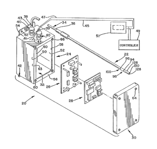
Reference numeral 20 of Figure 1 generally indicates
one embodiment of the air velocity transmitting unit or device
as a whole, which unit comprises probe 22 that contains the
unit or device sensing elements, the housing 24 that houses
both the unit transmitter circuit board 26 and t.he linearizer
circuit board 28, as well as the electronic components that
are respectively mounted on the respective boards 26 and
28, as well as the housing cover 30 that is normally employed
to close off the chamber 32 of the housing 24, and a suitable
cable 34 having one of its ends 36 suitably connected to .-.
probe 22 and the other of its ends 38 suitably connected
to the transmitter circuit board 26 through a suitable con-
ventional liquid tight connector indicated at 40. The housing
24 includes a suitable mounting plate 42 suitably secured
to the rear of same, for fixing housing 24 in a desired mounted .
position that may be adjacent to or remote from the air flow
that is to be measured by the unit 20, as will be apparent
to those skilled in the art. A second liquid tight connector
40 is applied to housing 24 for similarly accommodating a
suitable cable 39 containing in the usual electrically in-
sulated manner power supply conductors 41 and 43 and the
linearized signal conductors 45 and 47; the conductors 45
and 47, as diagrammatically indicated in Figure 1, are suitably
electrically connected to and between the circuit of Figure
13 and, for instance, when a device 20 is used in accordance
with the present invention, a conventional controller 49
and/or a conventional digital readout device 51 (provided
for either local or remote readout of the air velocity moni-
tored by a device 20). Cable 39 may be of any suitable type
11 3212~
having the requisite leads and may be spliced or otherwise
conventionally formed to provide the conductors 41, 43, 45,
and 47. The conductors 41 and 43 are connected between the
source of electrical energy and circuit 149 of Figure 6.
The housing 24 may be formed from a suitable metal
or plastic, and defines side walls 50 and 52, top wall 54,
front wall 56 that is suitable apertured to define a relatively
large access opening 58 for passing the circuit boards 26
and 28 therethrough to and from the chamber 32 of housing
24. The housing also defines rear wall 60 to which, for
instance, separate mounting plates 42 and 43 are suitably
affixed, as by welding or using screw type fastening devices
or a suitable adhesive. Mounting plates 42 and 43 may be
formed with a plurality of screw receiving apertures 62 or
the like for mounting the housing 24 in the position desired.
The housing cover plate 30 in the form shown is
suitably recessed or dished to be received over the front
6:3 of the housing 24 and is formed with suitable screw receiving
openings 64 that are spaced to be congruent with the threaded
screw receiving openings 66 of the housing 24, when cover
is received on the housing front 63, whereby the cover 30
may be secured to the housing 24 utilizing fastening screws
of any suitable type, to close off the chamber 32.
The circuit boards 26 and 28 may be of any conven-
t:ional type formed from one of the dielectric plastic materials
such as glass epoxy to which the electrical and electronic
components about to be described, and that are partially
diagrammatically illustrated in the showings of Figures 1
and 2, are suitably applied. Board-26 has spaced apart locking
132~ 2~
circuit board supports 70 suitably affixed thereto having
reduced externally threaded end portions 72 for being received
through the respective apertures 74 of the board 28 for securing
the board 28 to the board 26 by suitable nuts applied to
the respective shank end portion 72, when the unit 20 is
assembled. Board 26 is also formed with suitable apertures
76 for mounting same to the housi.ng rear wall 60, as by em- -
ploying suitable mounting screws and the like as well as
spacers that may be of a dielectric nature to electrically
isolate board 26 from housing 24.
When the circuitry that is diagrammatically illus-
trated in Figures 6 - 14 is assembled on the respective boards
26 and 28, the board 26 is suitably mounted within the housing
chamber 32 and its circuitry appropriately connected to the
the conductors 41 and 43l the probe wiring, and the electronic
components of board 28, after which the board 28 may be applied
to the indicated position on shanks 70 and secured in place.
Cover 30 may then be secured on housing 24 to close off chamber
32.
The probe 22 comprises an elongate tubular member
80 (see Figure 3) that is preferably formed from a suitable
corrosion resistant material such as stainless steel in which
is received a single printed circuit board 82, of elongate
configuration, on which is mounted the two sensinq electronic
elements of the unit 20. In accordance with the present
invention the circuit board 82 (the solder side, as distin-
guished from its component side, is illustrated in Figure
3) mounts conventional bead thermistor 84 (that is to be
operated in the self heated mode), and a conventional chip
thermistor 86, in the indicated respective circuit board
apertures 88 and 90. The circuit board 82 is suitably affixed
~2~2~
in position within the tube 80, as by employing adhesive
or the like, where indicated at 92, to dispose the respective
circuit board apertures 88 and 90 in alignment with aligned
apertures 94 and 96 formed on opposite sides of the probe
tube 80 (Figures 1 and 3 show opposite sides of tube 8),
whereby the probe tube apertures 94 and 96, and the respective
circuit board apertures 88 and 90 form air stream flow through
passages 98 and 100 (see Figure 1), respectively, that extend
transversely thereto. Resistor 214 of the thermistor control
circuit 190 (see Figure 7) is also suitably mounted on the
probe board 82 across the board aperture 101 (though the
latter is not part of air stream flow through passages of
probe 22, these being limtted to passages 98 and 100).
The circuit board 82 may be of any conventional
type 7 and defines suitable substrate 102 which has imprinted
or delineated on same in any suitable manner, on both sides
104 thereof circuiting 106, in which in the form shown, include
pads or terminals 108, 110, 112, and 113, and leads or traces
114 and 116 on the board solder side 104, and other suitable
leads or traces that may be necessary on the component side
(not shown)with the respective sensors 84 and 86 being connec-
ted in the probe circuitry in the manner diagrammatically
illustrated in Figures 4 and 7 and described herelnafter
and the respective terminals 108, 110, 112 and 113 being
connected to the respective lead wires 118, 120, 122, and
124 that are a part of the cable 34 and form conductors back
to the electronic circultry contained within the housing
50, with the connections involved being similarly dlsclosed.
The probe tube 80 at its air flow through passage
providing end 126 is suitably closed by a suitable press
~ ~2~266
or force fitted plug 128, formed from a suitable dielectric
material, such as nylon, that is received in the tube end
126 in plug fit relation thereto, with its head 130 in full
contact with the tube end rim 132 annularly thereabout.
When the unit 20 is not being used, or when a specific probe
of same is not being used, the probe end is preferably covered
with a close fitting cover 134 formed from vinyl or the like
and has its side wall 136 of sufficient length to extend
well beyond the pairs of ports 98 and 100 and close same
off, as when the unlt is not in use. The internal diameter
of the cover 130 is proportioned for frictional slip fit
application to the tube end 126. When a probe 22 is to be
used, the cover 134 is removed from its slip fit applied
relation shown in Figure 3 to open the respective sets of
through passages 98 and 100.
The cable 34 may be of any suitable type having
the requisite leads, and at its end 36, in the form illus-
trated, extends through suitable shrink tubing 142 that is
suitably shrunk against the end 144 of the probe tube 80,
or suitably connected to the tube 80 in any other convenient
manner, to present the cable conductors for appropriate solder
connection to the circuit board terminals or pads as indicated
in any convenient manner. Of course, the tube 80 may be
right angled, otherwise angled, or may be straight, as desired.
The probe in use may be mounted in suitable position
to monitor a particular air or other gas flow using a conven-
tional liquid pitot type mounting or the like.
Referring now to the power source and voltage regula-
tion circuit 1~9 of Figure 6, electrical power in a range
of from about 22 to about 28 volts of either direct current
11
~32~266
or alternating current at a maximum load of about 225 milliamps
conducted from a suitable external power source (not shown),
as by suitable conductors 41 and 43, is applied to the input
terminals 150 and 152 of conventional integrated diode bridge
154 which converts the direct current or alternating current
power to strictly a direct current power that is then applied
to conventional voltage regulator 156. In the circuit 149
the resistors 158 and 160 are connected in such a manner
that the voltage regulator 156 outputs a voltage of 18 volts
direct current (nominal) and functions as a source of supply
(provides current flow into a load for unit 20). Capacitors
162, 164, and 166 prevent unwanted oscillations by increasing
the circuit stability. Resistors 168 and 170 are of such
values and are connected in such a manner that a nominal
voltage of 4 volts direct current is applied to the noninvert-
ing terminal 172 of integrated circuit amplifier 174. The
4 volt direct current is referenced through PNP bipolar trans-.
istors 176 and 178 connected in a Darlington configuration
such that the 4 volt direct current is a 4 volt direct current
sinking supply. Capacitor 180 is for the same general purposes
as capacitors 162, 164, and 166. "Ground" is indicated by
reference numeral 182.
The circuit 149 is inside the housing 24 and is
suitably applied to the board 26, with the board 26 being
suitably spaced from the housing rear wall 60 by appropriate
spacers. As indicated, the conductors 41 and 43 of cable
39 are suitably connected to board 26 to power circuit 149.
Referring now to the thermistor control circuit
190 shown in Figure 7~ the thermistor 84 is a commercially
~3~12~6
available bead thermistor that is incorporated in the circuit
190 as one-half 192 of bridge leg 194, of a self excited
wheatstone bridge 196 (in subcircuit form), with the bridge
other leg 203 having its halves 198 and 199 made up by having
its sections 200 and 202 formed by resistors 204 and 206,
respectively; the other sensing component of bridge 196,
namely conventional and commercially available chip thermistor
86, is connected in series with resistor 208 across the junctions
220 and 222 of the bridge upper and lower legs 203 and 194.
The half 205 of bridge leg 194 includes its upper section
213 formed by resistor 214, and its lower section 212 is
formed by bead thermistor 84. Similar to the anemometer
of said U.S. Patent No. 4,537,068, the bead thermistor 84
is operated in a self heated mode at a predetermined constant
temperature, which in the illustrated embodiment is 200 degrees
C. The resistance value of the thermistor at the selected
operating temperature of same is determined, and the resistor
214 is selected to have a resistance half that value, with
the resistor 206 having a resistance that is twice the value
of the resistance provided by th~ resistor 204 in combination
with the resistor 208 and the thermistor chip 86. The amplifier
218 is arranged to have its inputs 217 and 219 connected
to the junctions 220 and 222 of the bridge upper and lower
legs 203 and 194. The error signal developed between these
two junctions causes the amplifier 218 to drive the transistors
224 and 226 to maintain the excitation to the bridge 196
to the value necessary to maintain the resistance of the
thermistor 84.
The thermistor chip 86 is provided to correct for
ambient air temperature variations; as the temperature of
13
1 3 2 ~
the air flow under test varies, the thermistor chip 86, which
is operated at ambient temperature ancl senses ambient tempera-
ture, changes resistance so that the current flow through
the bridge 196 is altered, which causes a change in the operat-
ing temperature o~ the bead thermistor 84. This in turn
causes the output signal (voltage across the bead thermistor
86) to change in e~ual but opposite directions to that of
the thermal error caused by the temperature variations.
Resistors 204 and 208 help provide a smoother temperatue
control for the chip thermistor 86. Resister 228 is provided
to provide a small initial current flow through the bridge
196 so that as the power is supplied the inputs of the amplifier
218 are suitably biased for proper operation.
Referring now to Figure 8, the probe output adjust-
ment circuit 230 accepts the voltage signal VTH (in terms
of voltage) from the thermistor control circuit 190, with
the signal involved then being applied to conventional inte-
grated circuit amplifier 232 that is conventionally configured
as a buffer in order to isolate the thermistor control circuit
190 from loading caused by the probe output adjustment circuit
230. The sourcing supply of circuit 149 is connected to
"ground" 182 through resistor 236, the resistor 238 of voltage
divider 239, and resistor 240, with conventional integrated
circuit amplifier 234 being connected to the resistor 238
to create a similar isolated signal, Vz (in terms of voltage),
with the signals VTH and Vz being applied to the respective
integrated circuit amplifiers 232 and 234, respectively,
through the respective sets of resistors 242 and 244, 246
and 248, such that the output of amplifier 249 is the signal
VI = VTH - Vz.
14
~32~2~6
The signal VI (in terms of voltage) is applied
to the non-inverting terminal 251 of integrated circuit ampli-
fier 250. The output voltage signal of amplifier 250 is
characterized by the equation VOUt = (1 plus the ratio of
the resistance of resistor 252 as compared to resistor 254)
(VI)~
The capacitor 256 is used to eliminate unwanted
oscillations by increasing the stability of amplifier 250.
The overall output voltage VOUt of circuit 230
= (1 plus the resistance of resistor 252 over the ratio of
the resistance of resistor 254) (VTH - Vz).
The signal Vz is used to alter the offset of the
signal VOut. The final VOUt voltage signal of circuit 230
is connected to the analog to digital input circuit 255 by
way of a suitable wire jumper (not shown).
Referring now to the analog to digital input circuit
254 of Figure 9, the voltage signal from the probe output
adjustment circuit 230 (VOut) is applied to the non inverting
output terminal 256 of conventional integrated circuit amplifier
258, with such signal being amplified according to the relation-
ship: the voltage at pin 6 of analog to digital converter
284 equals (1 plus the resistance of the resistor 262 or
264 or 266 or 268 divided by resistance of resistor 270)
(VOUt). Thus, the output signal of the amplifier 258 is
controlled by any one of the resistors 262, 264l 266, or
268, depending upon which "off-on" switch 272, 274, 276,
or 278 is in the closed or "on" relation. The capacitor
280 is employed to stabilize the amplifier 258 and to eliminate
unwanted oscillations. The diode 282 serves as a limit (5.lV)
on the output of the amplifier 258.
~ 3~ 26~
The "off-on" switches 272, 274, 276, and 278 when
in their respective closed positions allow separate gains
(and thereEore velocity ranges) to be independently selected;
obviously only one of the four switches 272, 274, 276 and
278 is moved to the closed position at any one time~ These
switches are part of a conventional dip mounted SPST switch
package, in a specific embodiment of the invention.
The output of the amplifier 258 (V6), which is
in the 0-5 DC volt range, as the respective switches 272,
274, 276, and 278 are successively opexated, is sent to pin
6 of a conventional analog to digital converter 284 (see
Figure 10). Analog to digital converters, of course, are
a familiar form of digital computer integrated circuit device,
as are digital to analog converters.
Referring now to Figure 10, the converter 284 changes
each signal that is present at its pin 6 to an eight bit
non-linear digital signal, and for this purpose the converter
284 employs a conventional successive approximation potentio-
metric ladder that is effective to convert the zero-5 direct
current voltage range signal to an eight bit digital output
signal. Resistor 288 and diode 290 provide a 2.5 volt reference
for converter 284, a five voltage sourcing supply being made
available for this purpose by conventional regulation of
the AC or DC power supply as per Figure 6, for instance,
as shown in Figure 14. Resistor 292 and capacitor 294 are
conventionally arranged to provide the converter 284 with
a suitable clock frequency, using resistors 292 and capacitor
294.
The capacitor 296 is used to stabilize the electrical
energy supplied to the chip of the converter 284. Outputs
1~2~ 2~
so-B7 are suitably and respectively connected to the respective
inputs of the eprom 298, as indicated in Figure 12.
Referring now to the analog to digital timing circuit
300 as shown in Figure 11 (see also Figure 10), the purpose
of circuit 300 is to disable the analog to digital converter
284 until the input signal to same, on start up of the unit
20, is stabilized. The voltage across capacitor 302 is initial-
ly zero when the power to the unit 20 is "turned on" which,
as indicated, provides a five volt DC sourcing supply that
is made available to the circuit 300, as indicated in Figure
ll. This condition means that transistor 304 is "turned
off" prior to the electrical power being made available to
the unit 20. With transistor 304 "turned off", this allows
the base 305 of transistor 306 to be pulled up to about the
5 DC volt supply through resistor 307, which in turn causes
the collector 308 of transistor 306 (which is connected to
pins 3 and 5 of the converter 284j, to be held to about the
5 volt level when the power to unit 20 is "off" and for appro-
ximately three to five seconds after it is turned "on".
As the capacitor 302 charges up to five volts DC, this causes
transistor 304 to "turn on", which effects the "turn off"
of transistor 306, having the effect of the voltage available
at pins 3 and 5 of the converter 284 to drop to about the
4 DC volt supply level.
Resistor 310, resistor 312, capacitor 302, and
diode 314 combine to provide the indicated delay of approxi-
mately 3-5 seconds. The diode 316 is used to insure the
discharge of the capacitor 302 after the power to the unit
20 is "turned off".
Referring now to the linearity correction circuit
320 of Figure 12, the data bits (Bo-B7) of the analog to
~32~
digital conversion circuit 286, that represent the output
signal of the analog to digital conversion circuit 286, are
separately connected in any convenient manner to the separate
address ports (Ao~A7) of the conventional eprom 298. Eprom
298 conventionally contains calculated data (calculated for
the present invention at calibration of unit 20) at each
of the address ports Ao-A7, which collectively form the digital
output shown schematically at the right hand side of the
showing of the eprom 298 as o through 07. The eprom data
at each of the indicated eprom address ports Ao-A7 is calculated -
and inserted into memory such that the digital output represented
as o through 07 changes linearly with air velocity. The
calculated data involved is generated or obtained at the
time of calibration of the unit 20. The eprom 298 operates
electronically to send the linear data involved to the digital
to analog conversion circuit 322 (see Figure 13).
For each velocity reading that has been calibrated
for the unit 20, a separate linearization calculation is
required. This in turn requires the use of off-on switches
to select which velocity range (and therefore linearization
calculation) is desired. That is the function of off-on
switches 324, 326 and 328, which in practice are a part of
the same package of dip mount switches that are found in
Figure 9. Resistors 330, 332, and 334 are used as "pulldowns"
to make sure that the range connector lines 325, 327, and
329 are at zero voltage when the respective switches 324,
326 and 328 are open.
Referring now to the digital to analog conversion
circuit 322 that is illustrated in Figure 13, the linearized
data from the linearity correction circuit 320 becomes the
input signal to the digital to analog converter 340, which
then changes the digital signal to an analog signal that
18
~32~ ~6~
is linear with air flow velocity. Amplifier 342 along with
transistors 344 and 346, and resistor 348 combine to make
a current sink 350 with the following relationship; the amperage
of the current sink is greater than the ratio of the voltage
output of the linear analog signal to the resistance of resistor
348, where the current sink 350 is drawn from the 18 volt
source (circuit 149). The indicated five volt sourcing supply
is connected to converter 340, amplifier 352, and amplifier
358 in the manner indicated in Figure 13. The conductors
45 and 47 are suitably electrically connected with current
sink 350 in any conventional manner to supply the needed
linearized signal to one or more pieces of equipment of the
type referred to in connection with the showing of Figure
1.
The amplifier 352, in this connection, is employed
to set the high limit of the current sink 350 (typically
20 milleamps), based on the value of the resistor 354 in
the voltage divider 356 that is comprised of resistor 357
and resistor 354. The amplifier 358 is to set the low limit
of the current sink 350 (typically 4 milliamps) based on
the value of resistor 360 of the voltage divider 362 comprised
of resistor 360 and resistor 364.
Referring now to the linearizer power supply circuit
370 shown in Figure 14, the voltage regulator 372 serves
to maintain a constant voltage of 5 volts in the signal above
the 4 volt sinking supply, that may be used as indicated
in Figures 10 - 13. The capacitors 374 and 376 are used
to remove unwanted oscillations of the output signal provided
by the circuit of Figure 14.
Figure 15 is a graph illustrating a typical non-
linear signal output from the unit velocity sensor compared
19
1~2~2~
.
to the linearized signal representing the output of unit
20 that is made avallable for controlling or record keeping
purposes for a particular air flow situation to which the
invention is applied.
The diode bridge 154 is preferably of the type
offered by General Instruments Corp., Discrete Semiconductor
Div. of Chicago, Illinois as its Part No. W005M, or its equiva- -
lent.
The voltage regulators 156 and 372 are preferably
of the type offered by National Semiconductor Corp. of Santa
Clara, California, as its Part Nos. LM317T and LM340T05,
respectively, or their equivalent, respectively.
The analog to digital converter 284 and the digital
to analog convertor are preferably of the type offered by
the said National Semiconductor Corp., as its Part Nos. ADC0804LCN
and DAC0832LCN, respectively, or their respective equivalents.
The bead thermistor is preferably of the type offered
by Fenwal, Incorporated, of Ashland, Mass., as its Part No.
GB385M43 or its equivalent~
The chip thermistor is preferably of the type offered
by Sensor Scientific Inc., of Fairfield, New Jersey, as its
Part No. SC103C2, or its equivalent.
The voltage dividers 239, 356, and 362 may be the
voltage divider offered by Bourns, Inc., of Riverside, Cali-
fornia, or its equivalent.
The dip mounted SPST switch package, referred to
with respect to switches 272, 274, 276, 278, 324, 326, and
328, is preferably of the type offered by Grayhill, Inc.,
of LaGrange, Illinois, as its Part No. 78B08, or its equiva-
lent.
The eprom 298 is preferably of the type offered
by Advanced Micro Devlces, Inc., of Sunnyvale, California,
132~ 2~.
as its Part No. AM2732~DG, or its equivalent; see alsc the
1986 data book of this company.
The remaining electronic components referred to,
such as the diodes, transistors, amplifiers and the like
are readily available from any company selling routine elec-
tronic components, such as the aforementioned National Semi-
ccnductor Corp., or Motorola Inc., of Phoenix, Arizona, for
example.
It will therefore be seen that the transmitter
unit of the invention is arranged to provide an output signal
that is linear with respect to the air velocity of an air
flow being tested in accordance with the invention; the specific
unit described and illustrated provides such linear slgnal
in terms of the familiar 4-20 milliamp signal that is the
milliamp range long familiar to this field of endeavor.
The invention also provides for the testing of
the air flow involved at three separate velocity ranges by
operating conventional "off-on" switches.
The output signal of the unit of this application
is independent of the temperature variations of the measured
air flow.
The probe is constructed to be i~sensitive to dust
and dirt, which allows the probe to be operated in harsh
operating conditions.
The unit disclosed herein can be powered by either
a direct current or an alternating current source of supply
of electrical energy.
The unit housing 24 may be made suitably waterproof
and dustproof in any conventional manner to protect the elec-
tronic circuitry it houses.
The foregoing description and the drawings are
given merely to explain and illustrate the invention and
13~2~6
the invention is not to be limited thereto, except insofar
as the appended claims are so limited, since those skilled
in the art who have the disclosure before them will be able
to make modifications and variations therein without departing
from the scope of the invention.