Note: Descriptions are shown in the official language in which they were submitted.
1 32 1 ~)4~
IN T~IE UNITED STATES
PATENT AND TRADEMARK OFFICE
PATENT APPLICATION
; FORMAT CONVERTER
BACKGROUND OF T~IE INVENTION
1. Field of the Invention
The invention generally pertains to digital data
communication systems. More particularly, the invention
relates to methods and apparatus which use bit mapping and
frame alignment techniques to (1) locate and extract sub-
rate circuit data originially placed into a high speed
serial bit stream in accordance with a first predefined sub-
rate circuit protocol, and t2) create a reformatted high
speed serial data output stream, with the extracted sub-rate
eircuit data inserted therein in aceordance with a second
predefined sub-rate cireuit protoeol. The methods and
apparatus set forth are particularly useful in converting
between a single stage time division multiplexed
data format and a two stage time division multiplexed
format, e.g., the CCITT X.50 and I.463 protocols.
1 321 648
2. Description of the Prior Art
State of the art digital data communication
switching systems are typified by the systems described in
applicant's U.S. Patents Nos. 4,852,089 and 4,975,695 issued
July 25, 1989 and December 4, 1990, respectively.
The systems taught in U.S. Patent No. 4,852,089 is
defined as having m slots of data per frame and n fragments
per slot to yield a total of m x n fragments per frame.
For example, the invention taught in U.S.
Patent No. 4,~52,0~9 permits a T1 Iine to be divided up
into 24 slots, each 64 Kbps wide, with 8 fragments being
defined per slot (each representing 8 Kbps bandwidth). This
yields 192 fragments with an 8 Kbps signalling channel left
on the T1 line. Bandwidth allocation is also contemplated
for 2.048 Mbps Inter Module Links ("IMLs") within a given
node, where 32 slots, each 64 Kbps wide, can be defined
(each again with eight 8 Kbps fragments).
Also taught in the U.S. patents are
means for allocating and deallocating bandwidth on the
communication lines of the system using bit maps, how to
1 32 1 64~
perform allocation in a manner which minimizes call
blocking, contention, etc., and how to interconnect Customer
Premise Equipmen-t (CPE) to the node oriented network via
User Interfaces (UI), Network Processors (NPs), Switch
Matrices (SMs), Network Interfaces tNIs), etc., via the IMLs
in a given node.
The systems taught in the U.S. paten-ts
support the CCITT I.4G3 standard for multiplexing of sub-
rate channels. Also, these systems have the capability of
switching fragment vs. slot packets, i.e., have an improved
switching granularity as compared with the 64 Kbps switch
granularity to which the I.463 standard was designed.
For the illustrative 32 slot, 8 fragments per slot
IML bandwidth scheme set forth hereinbefore, I.463 mandates
that sub-rate channels (defined herein as a 19.2 Kbps
channel or any submultiple thereof) be assigned to 64 Kbps
of bandwidth (a whole slot) before being transmitted to the
switch. According to the I.463 standardj two layers of rate
adaptation are performed to condition sub-rate channel data
to be transmitted in the 64 Kbps packets.
Given the improved switching granularity and
bandwidth allocation capabilities of state of the art
systems, such as those set forth in the referenced U.S.
patents, it was an object of applicant's copending Canadian
patent application Serial No. 612,398, filed September 21,
1989, entitled "Methods and Apparatus For Multiplexing Sub-
1 321 64'~
~ate Channels In A Digital Data Communication System",assigned to the same assignee as this invention, to improve
the efficiency of bandwidth usage over the I.463 standard
for sub-rate channel bandwidth alLocation. This copending
application is hereinafter referred to as the "Improved
I.463 Patent Application".
It was also an ob~ect of the Improved I.463
Patent Application to be able to fully use the switching
capabilities (granularity) of the communication system.
Since the inventions taught in the
U.S. patents made it possible to switch fragments of less
then 64 Kbps, it was recognized that it would be desirable
if sub-rate channel assignments were keyed to the
granularity of the switch which in turn could be ideally
matched to the choice of fragment size.
Reference may also be made to applicant's
copending Canadian patent application Serial No. 612,404,
filed September 21, 1989.
In short, the Improved I.463 Patent Application,
describes how to improve the efficiency of bandwidth usage
over the CCITT I.463 standard, for switching systems having
a granularity of better then 64 Kbps (e.g. 8 Kbps).
The efficiency of bandwidth usage over the I.463
standard is achieved (in tlle context of the illustrative
example set out above) by implementing a new rate adaptation
scheme in which sub-rate data channels are assigned to an 8
1 32 1 6~8
Kbps fragment, or multiples thereof. For example, a 2.4
Kbps channel is assigned to an 8 Kbps envelope, 9.6 Kbps is
assigned to two 8 Kbps envelopes, etc. Multiple envelopes
(each 8 Kbps wide) are then multiplexed effecting a
potential 8 fold improvement over existing methods and
apparatus for implementing the I.463 standard. In the
illustrative context, the key is to use the 8 Kbps
granularity of the switch rather then the I.463 standard of
assigning sub-rate data to a whole 64 Kbps slot.
The CCITT I.463 standard (and/or improved versions
thereof) are not in universal use in digital communication
systems that carry sub-rate circuits. The Japanese, for
example, utilize the CCITT X.50 recommendations (to be
reviewed in detail hereinafter) for formatting sub-rate
circuit data. If wide area networks are to include nodes
where different format criteria are observed, particularly
regarding the placement of sub-rate data in their output bit
streams, then methods and apparatus to support format
conversion in such a network need to be devised to make
communication between the users at these nodes possible.
SUMMA~Y OF T~IE INVENTION
Accordingly, it is an object of the invention to
provide methods and apparatus that permit nodes of a
communication network, in which different data formatting
1 32 1 6~8
criteria for sub-rate circuit data are in force, to be able
to communicate with one another.
It is a further object of the invention to provide
methods and apparatus for accomplishing the aforesaid
objective via frame alignment, buffering and bit map driven
reformatting;techniques.
It is still a further object of the invention to
provide methods and apparatus that perform the aforesaid
conversion (1) by locating and extracting sub-rate circuit
data, embedded in an input serial bit stream in accordance
with a first predefined protocol (used at the sending node),
and (2) by creating an output bit stream, destined for use
by the receiving (target) node, in which the extracted
circuit data is reformatted and inserted in accordance with
a second predefined protocol, (in use at the target node).
A further, more specific, object of the invention
i5 to provide a format converter that performs bidirectional
conversion between a single stage time division multiplexed
data format and a two stage time division multiplexed data
format (e.g. between nodes using the X.50 and I.463
recommendations).
In accordance with the teachings of the invention,
methods and apparatus are set forth which are operative to
convert between-a plurality of sub-rate data formats in the
following manner.-
1 321 648
First means are utilized to take sub-rate data,
embedded in a serial IML stream, -that is asynchronous with
respect to the target node, and identify the start of
received sub rate circuit information in the stream. Since
IML data is organized in terms of frames and channels, the
start of each IML frame must be determined in order to
locate the circuit data. The data is embedded in a discrete
portion of a frame, in accordance with a first predefined
sub-rate CCITT protocol (e.g., X.50).
Once the sub-rate circuit locations in the data
stream are identified, the input sub-rate circuit
information is aligned in memory means and operated on by a
bit map driven Format Conversion Module ("FCM"). The FCM
reassembles the sub-rate circuit information in accordance
with the sub-rate circuit data format protocol used by the
target node (e.g., I.~63) and then transmits (outputs) the
reformatted bit stream onto an outgoing IML.
According to the invention, the process is
bidirectional.
Furthermore, according to one embodiment of the
invention, the Format Convertor (FC) facilitates conversion
between a single stage time division multiplexed data format
and a two stage time division multiplexed format (e.g. X.50
and I.~63) by utilizing the aforesaid bit map driven format
conversion technique.
1 321 648
The invention permits great flexibility in network
system configuration. In addition, the invention permits
multiple channels of different format or frame alignments to
be converted simultaneously.
These and other objects and features of the
present invention will be understood by those of ordinary
skill in the art after referring to the detailed description
of the preferred embodiment of the invention and the
appended drawing.
r3r~IEF Dr~SCr~IPTION or~ E Dr~AWING
Figure 1 is a high-level functional representation
of a typical digital data communication network comprising
nodes interconnected by communication lines.
Figure 2 is a block diagram of one such node
showing a variety of communication paths both within and
outside of a given node.
Figure 3 is a functional block diagram of the
Format Converter (FC) that operates in accordance with the
teachings of the invention.
Figure ~ depicts the frame and multiframe
structure of an SD Type II data link.
13216~8
Figure 5 depicts the TDM sub-rate multiframe
structure for one 6~ Kbps channel.
Figure 6 depicts the conEiguration of a frame
alignment word associated with a given multiframe.
Figure 7 depicts the ISDN sub-rate structure of
one 6~ Kbps channel.
Figure 8 depicts the 80-bit frame structure for
one channel ISDN channel.
Figure 9 depicts the "O"s and "l"s forming the
framing structure in the ISDN context.
Figure 10 depicts the TDM data alignment process
supported by the illustrative embodiment of the invention.
Figure 11 depicts, in block diagram format, one
example of a Format Conversion Module (FCM) suitable for use
in implementing the present invention.
Figure 12 depicts, in block diagram form, the ISDN
data alignment portion of the illustrative TDM/ISDN format
converter.
1 32 1 648
Figure 13 depicts, in block diagram form, the ISDN
to TDM conversion process utilizing the invention.
Figure 14 depicts a portion of an exemplary bit
map for converting TDM into ISDN subrate data.
Figure 15 depicts aligned data RAM address
segments.
Figure 16 depicts an example of ISDN circuit
assignments within an IML frame.
DET~ILED DESC~IPTION
Figure 1 depicts a typical network consisting of
nodes 101, 102, 103 and 104 interconnected by communication
lines. Some of the nodes are shown as having CPE equipment
connected to them. (Node 101 is shown connected to CPE 105,
and node 104 is shown connected to CPE 106.) In practice,
any of the nodes may have CPE connected to them.
As for the type of sub-rate circuit data
formatting defined as standard at a given node, node 104
could, for example, be connected to user telephone equipment
in Japan where X.50 formatting conventions are followed;
while node 101 could be connected to user equipment in the
U.S. where I.463 formatting conventions are followed.
,
1321~:~48
Figure 2 depicts an example, in block diagram
form, of one node in a communications network like the one
depicted in FIG. 1.
For sake of illustration, three Switch Matrices
110, 120 and 130, for example wideband time-slot switches,
are each shown connected, via bidirectional serial links, to
a plurality of User Interfaces (UI) 112, 122 and 132 and a
plurality of Network Interfaces (NI) 111, 121, 131. In
addition, SM 110 is shown connected via a bidirectional
serial link to Network Processor (NP) 140 and Packet
Processor (PP) 150. SM 120 is connected via a similar data
link to NP 141 and PP 151.
It should be understood that the disclosed system
is highly flexible and modular and the depicted system was
chosen for simplicity and clarity of presentation. It is
but one example of many possible combinations of these
components. A greater or lesser number of switch matrices,
network processors, packet processors, user interfaces and
network interfaces could have been chosen to depict the
system. The specific design of an individual system depends
on the particular data, voice and other requirements placed
on the node. For example, a system handling a large amount
of packet switching could require more packet processors,
but fewer switch matrices. Similarly, a system handling a
11
1 321 64~
large amount of circuit switching t:raffic could require a
larger number of switching matrices, but only one packet
processor.
Since the three switch matrices in the
illustrative node, and their interconnections, are
substantially identical, only SM 110 will be discussed in
detail. SM 110, in a preferred embodiment, contains 16 I/O
ports to accommodate up to 16 data links. Other numbers of
I/O ports could have been chosen for the switch matrix. As
discussed below, these 16 I/O ports may be individually
connected to a user equipment interface, a network equipment
interface, a packet processor, a network processor, another
switch matrix or, if appropriate to the system, a special
purpose format convertor (1~0) or an interface to an
external processor (190). In this embodiment, all data
links operate at 2.048 Mbps. It will be understood by those
of ordinary skill in the art that different data rates could
have been used.
User Interface 112 contains the logic to receive
voice, data and fax information from various Customer
Provided Equipment (CPE) 115 and perform the necessary
formatting, multiplexing, buffering and switching functions
to provide the user data to SM 110. Each UI 112 also
contains the logic to receive data from SM 110 and perform
the necessary formatting, demultiplexing, buffering and
t 32 1 648
switching functions to provide the data to the appropriate
user I/O device.
Each NI 111, for example a T1 interface, contains
the logic to receive data from SM 110 and perform the
necessary formatting, demultiplexing, buffering and
switching to provide the data to the appropriate network
(not shown). Each NI 111 also contains the logic to receive
data from the network and perform tlle necessary formatting,
multiplexing, buffering and switching functions to provide
data from the network to SM 110. SM 120 and 130 are
similarly connected to User Interfaces 113 and 11~
respectively and to Network Interfaces 121 and 131
respectively.
In the disclosed embodiment, close physical
proximity of the switch matrices allows for the use of a
high bandwidth backplane bus 170 to handle communications
among switch matrices. This eliminates the need for
dedicating a portion of the switch matrix I/O ports to
communication among switch matrices and frees the ports for
user traffic. The use of a high bandwidth bus also has the
advantage of providing sufficient bandwidth to allow
additional switch matrices, and therefore, additonal user
and network interfaces, to be incorporated into the system.
If desirable in a particular system, however, communications
among switch matrices could be handled via data links.
1321648
The Network Processor provides the appropriate
commands and information to establish and terminate the
approporate Switch Matrix connections to accomplish the
requested informaiton transfer. The Packet Processor
operates as a "level 2" protocol translation processor and
is responsibie for creating, formatting and controlling the
transfer of information according to the desired protocol
standard. As discussed above, the switch matrices are
connected via data links to the Network Processors and the
Packet Processors. - -
To provide overall coordination of the
interconnection of the system components, one of the network
processors must function as a "master". This requires that
the master must be informed of, and retain a record of, all
switching connections established not only by itself, but
also by the other network processors. As can be seen from
FIG. 2, each of the network and packet processors needs to
be directly connected via a data link to only one of the
switch matrices. NP 140, in this emboidment, is connected
via data link only to SM 110. Switching commands or other
information from NP 140 to one of the other switch matrices
is passed through SM 110 via bus 170 to SM 120 or SM 130.
In addition to being connected to the switch
matrices by data links, each network and packet processor
14
1 321 64g
can communicate with each other processor via a standard
parallel processor bus 160. Memory 161, for example, a hard
disk, and other processing resources may be attached to bus
160 and accessed by the processors over bus 160.
The operation of the illustrative network and node
briefly described hereinabove, is more fully described in
U.S. Patent No.
4,852,089. Also, the operation of such a network with an
Improved I.~63 sub-rate channel rate adaptation scheme,
permitting up to three 2.~ Kbps sub-rate circuits to be
embedded in an 8 Kbps envelope, is set forth in
Canadian patent application Serial No. 61~,i9~.
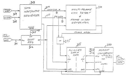
FIG. 3 is a functional block diagram of a Format
Converter (FC), shown in FIG. 2 as format converter 180,
that operates in accordance with the teaching of the
invention.
Before detailing the operation of the depicted FC,
two specific CCITT formats will be described along with the
general functional requirements of the FC that is capable of
converting between these two formats. This description will
lay a foundation for describing the more general invention
functionally depicted in FIG. 3, but is not meant to limit
1 321 64~
the invention to methods and apparatus for converting only
between the illustrative formats.
The FC used to teach the invention is a TDM X.50/
ISDN (bidirectional) Format Converter suitable for use as
part of a digital communication system. For the sake of
illustration only, one part of the system is defined to use
the CCITT I.463 ISDN sub-rate data format for its internal
data communication; while another part of the system uses
the X.50 convention. The FC allows non-ISDN compatible
equipment (such as X.50 compatible equipment) to be coupled
to the I.463 oriented part of the system.
The details of the sub-rate formats operated on by
the FC that is used herein to teach the invention, will be
reviewed first for the sake of completeness before
describing the details of the format converter structure per
se.
The TDM sub-rate data format referred to
hereinabove conforms to the CCITT recommendations X.50.
Again, this sub-rate format is used, for example, by the
Japanese in their Super Digital Type II link.
In a preferred embodiment of the invention, the FC
is designed to have a 480 circuit capacity since a Super
Digital Type II interface can handle 480 2.4 Kbps circuits.
13~1648
As a result, in one application of the invention, one format
converter is capable of servicing one Super Digital Type II
interface. Circuit capacity vs. sub-rate data format is
discussed more fully hereinafter.
For the sake of illustration only, the invention
will be set forth in the context of a switching system where
the basic sub-rate circuit is 2.4 Kbps. The illustrative
sub-rates will be 2.4, 4.8, 9.6, and 19.2 Kbps. In addition
to these sub-rate circuits, the invention handles 48 and 56
Kbps circuits. These circuits are confined to one 64 Kbps
information channel and do not span multiple 64 Kbps
channels. This is because synchronization between channels
can not be guaranteed. Both ISDN and TDM links carry
circuits above 19.2 Kbps. At these rates, only one circuit
occupies the 64 Kbps channel, and the sub-rate structure is
not used. The preferred YC will pass these higher rate
circuits with the proper signal and framing bits required of
each format.
The sub-rate formats for the illustrative
embodiment of the invention will now be described.
Super Digital ("SD") is a term used to describe
the Japanese Type II data link. The SD Type II structure is
very similar to the U.S. Tl link. The bit rate is 1.544
Ml~z. Each frame is 125 microseconds wide and is composed of
1 32 1 648
193 bits. The first bit is for link overhead, and the
remaining 192 bits are organized into 24 channels of eight
bits each. Each channel is a 64 Kbps information channel.
The frames are grouped into multiframes of 24 frames each.
The first frame in the multiframe is indicated by a coding
violation in the link overhead bit. The frame and
multiframe structure of the SD Type II link is shown in
FIG. 4.
The TDM sub-rate format embeds twenty 3.2 Kbps
circuits within a 64 Kbps TDM channel per CCITT
~ecommmendation X.50. The l'DM Type II link can contain up
to twenty-four multiframes. The multiframe is not
synchronized to the starting frame of the TDM links. As a
result, framing information must be embedded in the
multiframe itself. One of the eight bits in the 64 Kbps
channel is reserved for a framing bit. Figure 5 shows the
TDM sub-rate multiframe structure for one 64 Kbps channel.
Each sub-rate frame contains the following bits:
(a) F = frame synchronization bit (X.50 pattern)
(b) S - state bit (1 = data valid, 0 = data not
valid)
(c) D `- 6 bit circuit data
18
1 32 1 648
Each 2.4 Kbps circuit occurs every 20 frame
periods or 2.5 m sec. The data rate for each frame is 3.2
Kbps (8 bits / 2.5 m sec). The information rate for the
circuit data (6 bits) is 2.4 Kbps (6 bits / 2.5 m sec).
The "F" bits are used to deframe the multiframe
circuit data. The FC will ignore the "S" bit information.
The "S" bits will be set to a default value of "1" in
outgoing TDM data. The "D" bits are the circuit data, which
need to be reformatted.
The multiframe has a 20-bit frame alignment word
embedded in it. The "F" bit of the sub-rate data is used to
form this word. The frame alignment word (FAW) is
configured as shown in FIG. 6.
According to X.50 format, the first bit of the FA~
is an alarm blt. An alarm condition occurs when there is an
absence of incoming pulses, or a loss of frame alignment.
The FC will detect an alarm condition and note its
multiframe channel number. This information can be passed
onto, for example, a node processor in the switching system.
Outgoing "A" bits can be set to either alarm or no alarm
condition.
19
1 32 1 6~
The "F" bit will always occur in bit location 1 of
the sub-rate multiframe. }lowever, each multiframe in a TDM
multiframe is aligned independently of any other multiframe
in the link. ~lignment of one multiframe does not guarantee
alignment of any of the other 23 multiframes. Deframing
data in a TDM multiframe must be done on an individual
multiframe basis.
It should be noted that since the basic sub-rate
circuit is 2.4 Kbps and a sub-rate multiframe will contain
twenty 2.4 Kbps circuits, higher circuit rates can be
obtained by combining multiple 2.4 Kbps cirucits to form a
high information rate circuit. The following rates are
available using this technique:
Circuit Rate Circuits/Multiframe
2.4 Kbps 20
4.8 Kbps 10
9.6 Kbps 5
19.2 Kbps 2
48.0 Kbps
56.0 Kbps
64.0 Kbps
1 32 1 64~ ;
Ayain, this technique is restricted to one 64 Kbps
channel, since there is no method to insure synchronization
between multiple 64 Kbps channels.
}laving reviewed the Japanese TDM sub-rate format,
the ISDN format will now be described.
The ISDN sub-rate splits one 64 Kbps channel into
a maximum of eight 8 Kbps channels. The ISDN subrate
structure of one 64 Kbps channel is shown in FIG. 7. The
basic ISDN granularity is 8 Kbps.
Each channel carries one circuit. The circuit
information is arranged into an 80-bit frame squence. The
frame sequence contains framing information, circuit rate
information, and signalling information, as well as the
circuit data. Unlike the TDM multiframe subrate structure,
there is no embedded frame structure required to break out
individual circuits. The 80-bit frame structure for one
channel is depicted in Fig. 8.
The FC will ignore incoming "S", "X" and "E" bits.
Outgoing "S" and "X" bits are set to default values of "1".
The "E" bits are set to the proper circuit rate value.
The ISDN sub-rate data is transmitted as an 80-bit
serial data stream, starting with Octet 0 - bit 0 and ending
t 32 1 64~
with Octet 9 - bit 8. The "0" and "1"5 form a framing
structure as shown in FIG. 9.
The basic 80 bit frame structure, shown in FIG. 8,
can support several circut sub-rates. The maximum sub-rate
for an 8 Kbps channel using this frame structure is 4.8 Kbps
(48 bits / 10 m sec). Slower circuit rates are implemented
by repeating circuit data among the "D" bits. For example,
a 2.4 Kbps circuit will use all 48 "D" bits, but will repeat
data for every 2 "D" bits, giving an effective "D" bit
number of 24 data bits per frame (2.4 kbps = 24 bits / 10 m
sec). Conversely, higher circuits rates can be obtained by
combining multiple 8 Kbps channels. The sub-rates become
multiples of 4.8 Kbps. The following rates are available
using this technique.
Circuit Rate CircuitsJ64 Kbps Channel
2.4 Kbps 8 ( 8 Kbps channel)
4.8 Kbps 8 ( 8 Kbps channel)
9.6 Kbps 4 (16 Kbps channel)
19.2 Kbps 2 (32 Kbps channel)
48.0 Kbps 1 (64 Kbps channel)
56.0 Kbps 1 (64 Kbps channel)
64.0 Kbps 1 (64 Kbps channel)
1 321 648
A serious problem exists between the ISDN and TDM
subrate formats: circuit capacity per 6~ Kbps channel. The
circuit capacity of both sub-rate formats is repeated here:
Circuit ~ate Circuits/64 kbps Channel
SD ISDN
2 . 4 Kbps 2 0 B \
4 . 8 Kbps 10 8 TDM greater than ISDN
9.6 Kbps 5 4 /
19. 2 Kbps 2 2 \
48 .0 Kbps 1 1 \ TDM equal to ISDN
56.0 Kbps
64 .0 Kbps
For low rate circuits (9. 6 Kbps and below) the TDM
subrate format has greater circuit capacity than ISDN.
Extra ISDN channels are required to equal the circuit
capacity of the TDM channels. As a practical matter, extra
channels may not be available. As a result, the preferred
FC and conversion process contemplates a worst case
situation and limit their performance to the capacity of the
ISDN sub-rate format.
Having reviewed an illustrative context in which
the invention is to operate, the format converter itself
will now be described with reference to FIG. 3.
1 32 1 648
For the sake of illustrating the invention, it
will be assumed that an IML stream, with embedded X.50
formated sub-rate circuit data, is input to the format
converter on link 301. This is shown coming from the switch
matrix as shown in FIG. 2.
~ 11 of the teachings to be set forth hereinafter
support an FC with a bidirectional operating capability,
i.e., for the example of an X.50/I.463 converter, I.463
formatted sub-rate data could just as well be embedded in
the input IML stream. The difference would be the structure
of the bit map driving the conversion process and in the
synchronization detection process, to be explained in detail
hereinafter with reference to FIG. 12.
The invention contemplates a programmable bit map
to support conversion between a plurality of format
protocols.
The data input on link 301 is shown clocked into
shift register 302, via a 20~8 Khz clock signal output by
data input/output sequencer 303 on link 304.
Data input/output sequencer 303 is shown receiving
a frame synchronization signal and 4096 Khz clock input
signal from an external synchronization and control device
(not shown in Fig. 3). The synchronization and control
device is nothing more than a timer which sends a framing
signal and 4096 Mhz clock signal to device 303.
24
1 32 1 648
The function of device 303 is to provide basic
timing and control for the TDM and ISDN data input/output.
Unit 303 is shown to accept the two 20~8 Khz clock signals
and a frame synchronization signal from an external timing
un-it. These signals are depicted as being input to unit 303
on links 308 and 309 respectively. Unit 303 generates a
properly phased 2048 Khz clock signal for control of the
input IML channel (via link 304), a data strobe (load) on
link 315, and a current address value (shown as channel
number and frame number in FIG. 3 on links 350 and 351
respectively) which is used to segregate data into the
proper channel frame and bit location postitions for storage
in aligned data memory 325. This procedure will be
explained in greater detail hereinafer.
The conversion process itself consists of two
steps: (a) storing the incoming TDM multiframe data from
the IML input into the aligned data memory (preferably a
RAM); and (b) conversion of TDM data to ISDN data, based on
a bit mapping conversion scheme.
The input TDM data is written directly into the
aligned data RAM using an address offset (or indexing)
scheme. FIG. 3 and 5 illustrate this process.
The objective of this process is to store all the
incoming data into the aligned memory where all the
multiframes (for TDM data) are organized as shown in FIG. 5
(i.e., circuit number one is located in frame number one,
t 32 1 648
circuit number two in frame number two, etc.). This process
is necessary since the incoming TDM multiframes are not
aligned to each other. Since the format conversion process
uses a bit mapping scheme, it is important to store the TDM
data into known locations for this process to work.
A parallel processing circuit, shown in FIG. 3 as
Sync Detect and Frame Index Generator 310, examines the
multiframe data for the starting postions of each of the 31
TDM multiframes. The starting position is identified as the
"Frame Index". The "Frame Index" is generated, according to
one embodiment of the invention, when the framing word for a
TDM multiframe has been detected at least three times in a
row at the same frame location. The "Frame Index" is an
address offset value which when added to the Current Address
value (shown at block 355 of FIG. 3) will place the TDM
multiframe data into the correct location of the Aligned
Data Memory.
The Frame Index value is added to the Current
Address value to form the Align Frame value. Figure 10
illustrates this process. The Initial TDM multiframe
placement is offset by the Frame Index value to create the
Aligned TDM multiframe data.
It will be recognized by those skilled in the art
that each of blocks 302, 303, 310, 325 and 355 of FIG. 3 can
26
1 321 ~48
be realized by either conventional off-the-shelf logic or
well known methods and apparatus for performing
synchronization and framing. Units 302 and 355 can be
realized by a standard 8 bit shift register, and an adder,
respectively. Unit 303 can be realized by a counter chain
controlled by the external frame synchronization and clock
signals. Unit 350 can be a RAM and unit 310 can be realized
by well known methods and apparatus for synchronizing an
asyncllronous serial bit stream that inherently contains
framing information.
Once the incoming data is stored in the aligned
data memory the illustrative TDM to ISDN conversion can be
accomplished using the bit map and a readout sequencer to
output data in the ISDN format. This is depicted in FIG. 3
as taking place in the format conversion module (FCM), unit
380, and is described in detail hereinafter with reference
to FIG. 11.
According to the preferred embodiment of the
invention the output data is formatted a byte at a time.
The bit map contains a 80 frame mapping sequence, which
conforms to the ISDN format. The proper circuit data
placement, as well as the framing bits ("0", "1"), the "S"
and "X" bits (defaulted to "1"), and the proper "E" bit
information, are also contained in the map. FIG. 11 depicts
this process in simple block diagram form.
27
1 32 1 6~8
FIG. 11 shows an example of the FCM where, in
accordance with one embodiment of the invention, the bit map
(unit 385), a bit latch (unit 386) and a shift register
(unit 387) are all within the FCM. Those skilled in the art
will recognize that, for example, units 386 and 387 could be
located outside the FCM without departing from the spirit
and scope of the invention.
The bit map contained in the ~CM is driven by the
current address value output by unit 303 as shown in FIG. 3.
Based on the current address input to the FCM, the
bit map knows what the next outgoing ISDN data byte should
be comprised of. The bit map loads up the next outgoing
ISDN data byte into the bit latch. The proper circuit data
bits are picked from the aligned data RAM and stored into
the proper byte position in the bit latch. The load strobe
from unit 303 will load this valued into the shift register
at the appropriate time and the data will be clocked onto
the IML bus (shown in FIG. 3 at 399).
Bit maps for each sub-rate conversion circuit can
be, for example, stored in ROM. Templates can be
constructed to suit any protocol involved in the conversion
process. The bit map are programmable presenting to the
28
1 32 1 ~j48
user a very high degree of flexibility in designing format
conversion optlons.
The preferred embodiment of the FC performs
conversion in the ISDN to TDM direction as well. This
process is generally the same as described hereinabove for
the TDM to ISDN direction but detailed differences lie in
the synchronization detection process and bit map structure,
as will be explained hereinafter with reference to FIG. 12.
The ISDN data is written directly into an Aligned
Data RAM using an address offset (or indexing) scheme.
Figure 12 illustrates this process. The objective of this
process is to store all the incoming ISDN data into the
depicted Aligned Data Ram, 1205, where all the ISDN circuit
data is placed into known locations, (i.e., Circuit #1 -
Data Bit #0 is placed into Aligned RAM 1205, location #0 -
Bit #0). This process is necessary since the incoming ISDN
circuits are not aligned to each other. Since the format
conversion process uses a bit mapping scheme, it is
important to store the ISDN data into known locations for
this process to work.
A parallel processing circuit, referred to
hereinafter as ISDN Circuit Detect and Index Generator 1206,
examines the ISDN circuit data for the starting positions of
each of the 256 possible ISDN circuits. The starting
1 32 1 648
position is identified as the "Circuit Index". The "Circuit
Index" is generated, according to the preferred embodiment
of the invention, when the framing structure for an ISDN
eircuit has been detected at least three times in a row at
the same location. The "Circuit Index" is an address offset
value which when added to the Current Address value will
place the TDM multiframe data into the correct location of
the Aligned Data RAM.
Figure 12 is a simple block diagram of the ISDN
Data Alignment portion of the ISDN to TDM conversion
eircuit. Again, as with FIG. 3, the components and frame
detection methodology depicted in FIG. 12 are well known to
those skilled in the art.
The actual ISDN to TDM eonversion is aeeomplished
using a bit map and a readout sequencer to output data in
the TDM format. The output data is formatted a byte at a
time. The bit map contains an 80-frame mapping sequence,
whieh eonforms to the TDM format. The proper mapping
sequenee, whieh eonforms to the TDM format. The proper
eireuit data plaeement, as well as the framing bits ("0"),
"1") and the "S" bits (defaulted to "1"3 are also eontained
in the map.
Figure 13 is a simple bloek diagram of this
proeess. Bit map 1~01, is driven by the Current Address
1 321 648
value from the data input/output sequences (e.g. unit 303 of
FIG. 3). Based on this input, the bit map knows what the
next outgoing TDM data byte should be comprised of. Bit map
1301 loads the next outgoing TDM data byte into Bit Latch
1310. The proper circuit data bits are picked from Aligned
Data RAM 1325 and stored into the proper byte position in
Bit Latch 1310. The LOAD strobe from sequencer 303 will
load this value into Shift Register 1340 at the appropriate
time and the data will be clocked onto the IML bus.
~ gain bit map templates for each sub-rate circuit
conversion can be stored, for example, in ROM.
To conclude this detailed description of the
invention, since the format conversion process is dependent
upon the use of bit mapping techniques, an explanation of
the bit mapping format conversion process will be set forth
hereinafter for the sake of completeness.
Bit map operation is explained hereinafter by way
of example. This example considers only one 64 Kbps
channel. The format conversion will transform TDM into ISDN
sub-rate data. Figure 1~ illustrates the first 20 frames of
stored TDM data in the Algined Data RAM and the first 20
frames of the outgoing ISDN data.
1 32 1 6~8
The TDM data, which resides in the Aligned Data
RAM, was stored into R~M according to its position in the
IML frame. The Aligned Data RAM address is segmented using
IML position data as shown in Figure 15.
The ISDN data, shown in Figure 1~ is arranged by
its postion in the outgoing IML frame. Channel, Frame and
Bit # are determined by the Current Address. The data for
ISDN circuits 1-8 reside in the TDM Aligned Data R~M (frames
0-7). This information must be retrieved from the Aligned
Data RAM at the proper time.
As an example, assume the Current Address =
Channel 1, Frame 12. Referring to Figure 14, one can see
that the outgoing ISDN data byte at this Current Address
location is composed of TDM circuits 1 through 8, bit D2.
Referring again to Figure 14, the data for the eight TDM
circuits can be seen to reside in the Aligned Data RAM at
frame locations 0-7, bit location 2. A lookup table can be
generated for Current Address vs. Aligned Data RAM Address.
For this example the table is:
Circuit - Bit Current Address Aligned Data RAM Address
# # Channel Frame Bit Channel Frame Bit
1 D2 1 12 0 1 0 2
2 D2 1 12 1 1 1 2
3 D2 1 12 2 1 2 2
- 1321648
4 D2 1 12 3 1 3 2
D2 1 12 ~ 1 ~ 2
6 D2 1 12 5 1 5 2
7 D2 1 12 6 1 6 2
8 D2 1 12 7 1 7 2
This table is the basis for the bit map. Let:
a. BIT MAP ADD~SS = CURRENT ADDRESS
b. BIT MAP DATA = ALIGNED DATA RAM ADDRESS
The Bit Map becomes a lookup table of Current
Address vs. Aligned Data RAM Address. When the Bit Map is
presented with a Current Address, it will produce the
corresponding Aligned Data RAM Address needed to retrieve
data from the Aligned Data RAM.
The Bit Map address and data words are segmented
according to the channel, frame and bit values. An example
is given here:
BIT MAP ADDRESS: [----------Current Address----------]
Channel # Frame # Bit #
ADDRESS = A12 All A10 A9 A~ A7 A6 A5 A~ A3 A2 Al AO
1 32 1 648
IT MAP DATA: [--------Aligned Data RAM Address------~]
Channel # Frame # Bit #7
DATA = A12 All A10 A9 A8 A7 A6 A5 A4 A3 A2 Al A0
Using this manner of Bit Map Address and data wor~
assigments the lookup table generated for Current Address
vs. Aligned Data RAM Address is stored in the Bit Map as
follows:
Circuit - Bit BIT MAP
# # ADD~ESS DATA (hex)
1 D2 0160 0103
2 D2 0161 OlOB
3 D2 0162 0113
4 D2 0163 OllB
D2 0164 0123
6 D2 0165 012B
7 D2 0166 0133
8 D2 0167 013B
The Bit Map provides the cross-connection between
TDM and ISDN circuits. The connection plan function is
inherent in the Bit Map operation since the Bit Map can
34
1 32 ~ 648
place incoming circuit data anywhere in the outyoing IML
data stream.
TDM circuits are defined by IML channel assignment
and circuit sub-rate. The circuit sub-rate information
defines where the circuit data resides within a TDM
multiframe as illustrated in FIG. 14.
ISDN circuits are defined by IML postion and
circuit sub-rate. Unlike TDM circuits, each ISDN circuit
resides within a 8 Kbps (or multiple 8 Kbps) channel.
Circuits of difference sub-rates are allowed to coexist
within one 64 Kbps channel As a result the IML position
must include channel position AND position within the
channel (bit location).
An example of ISDN circuit assignments is shown in
Figure 16.
Once the TDM and ISDN circuit locations are
established, the connection between the two must be
established (i.e., TDM Ckt # 23 = ISDN Cirucit ~ 210). This
information can be sent to the FC from the network
processor. According to the illustrated embodiment of the
invention, three rules for the connection plan are:
a. TDM data collected into one 64 Kbps channel MVST be
1 3~ 1 648
of the same circuit subrate.
b. ISDN data which is of multiple 8 Kbps channels MUST
reside within the same 6~ Kbps channel and occupy
consecutive 8 Kbps channels.
;
c. TDM and ISDN circuits which are connected must be
of the same circuit sub-rate.
The actual Bit Map provides both circuit cross
connect and format conversion. The Bit Map is, according to
the invention, loaded with the proper circuit sub-rate
~onversion templates according to the arrangement of the
outgoing circuit sub-rate characteristics. ~n example of a
circuit sub-rate conversion template is given in Figure 1~.
It provides the basic format conversion plan between TDM and
ISDN sub-rates for one circuit sub-rate.
What has been described herein is a Format
Converter that supports TDM/ISDN format conversion. The
converter described is bidirectional. Those skilled in the
art will recognize that the FC is programmable, i.e.
modifying the templates will yield different format
conversion results.
Those skilled in the art will also recognize that:
36
1321648
(a) the invention supports bidirectional
conversion between ,a single stage time
division multiplexed data format and a two
stage time division multiplexed format, and
more generally that
(b) the invention supports conversion between
first and second predetermined protocols for
embedding sub-rate circuit data in a high
speed serial bit stream.
All of the aforestated ob~ectives of the invention
are met by the methods and apparatus described hereinabove.
Those skilled in the art will recognize that the foregoing
description of a preferred embodiment of the novel methods
and apparatus has been presented for the purposes of
illustration and description only. It is not intended to be
exhaustive or to limit the invention to the precise form
disclosed, and obviously many modifications and variations
are possible in light of the above teaching.
The embodiment and examples set forth herein were
presented in order to best explain the principles of the
instant invention and its practical application to thereby
enable others skilled in the art to best utilize the instant
132164~ ~
invention in various embodiments and with various
modifications as are suited to the particular use
contemplated.
It is intended that the scope of the instant
invention be defined by the claims appended hereto.
38