Note: Descriptions are shown in the official language in which they were submitted.
- 1 - 1 321 660
SEMICONDICTOR DEVICE
BRIEF DESCRIPTION OF THE DRAWINGS
Fig. 1 is a schematic diagram of a semiconductor device
comprising a pin-type semiconductor layer and explaining
the first aspect of the present invention;
Fig. 2 is a schematic diagram of a semiconductor device
comprising a pin-type semiconductor layer and explaining
the f irst aspect of the present invention;
Fig. 3 is a view explaining an embodiment of a semi-
conductor device of the second aspect of the present
invention;
Fig. 4 is a view explaining an embodiment of a conventional
semiconductor device;
Fig. 5 is a view explaining an example of the
distribution of dopant in a pin-type semiconductor layer ~-
used in the second aspect of the present invention and an
example of the distribution of dopant in a conventional
pin-type semiconductor layer;
Fig. 6 is a graph showing a V-I characteristic of
solar cells obtained in Example 12 and Comparative Example
2;
Fig. 7 is a sectional view of a semiconductor device
in Example 13 of the third aspect of the present invention;
Fig. 8 is a graph showing a V-I characteristic of
semiconductor devices in Example 13 and Comparative
Example 3; and
Fig. 9 is a sectional view of a conventional semi-
conductor device.
BACKGROUND OF THE INVENTION
The present invention relates to a semiconductor
device, and more particularly to a semiconductor device
comprising a photovoltaic device having high open-circuit
..
- - 2 - 1 32 1 660
voltage under light irradiation or a photovoltaic device of
which photoelectric conversion efficiency is improved.
Hitherto, as a material for photoelectric converters
such as solar cells, there has been used a semiconductor
material comprising amorphous semiconductor such as a-Si:H,
a-Sil_x:Cx:H, a-Sil_xGex:H, a-Si:F:H, a-Sil N H, a-Ge:H,
a Si Ge :F:H, a-Si:H, ~c-Si:H, ~c-Sil_xGex:~ (whe
satisfies the relationship of 0~x<1) or semiconductor
material containing partially such amorphous semiconductor.
A conventional solar cell has a laminated structure
of pin, nip, pinpin... or nipnip... obtained by depositing
ln order the same kind of amorphous semiconductor or different
~ind of amorphous semiconductor having wide energy gap
only in its doping layer. The density of dopant in p-type
or n-type layer is uniform throughout a direction of the
thickness of the layer except the distribution of dopant
due to thermal diffusion during and after the production of
the device, and it is usually 0.01 to 5 atm %.
Fig. 9 shows a semiconductor device employed in a
conventional solar cell using-pin-type semiconductor of
triple layer construction. In Fig.9, numeral 31 is a glass
substrate whereon a transparent electrode 32 is attached.
On the transparent electrode 32, there are formed a p-type
semiconductor layer 34, i-type semiconductor layer 35 and
n-type semiconductor layer 36 in order. Further, on the
n-type semiconductor layer 36, there is formed an electrode
37. The semiconductor device 38 consists of a glass substrate
31, a transparent electrode 32, a p-type semiconductor layer
34, an i-type semiconductor layer 35, an n-type semiconductor
layer 36 and an electrode 37.
~ J
,
- 3 - 1 321 660
.~
In the above semiconductor device 38, light enters
the glass substrate 31 along a direction of arrows in Fig. 9,
is transmitted through the glass substrate 31 and the elect-
rode 32, and then irradiates the p-type semiconductor layer 34,
i-type semiconductor layer 35 and n-type semiconductor layer
36. By this irradiation, pairs of electrons and holes are
generated in each semiconductor layer 34, 35 and 36. Then,
electrons are collected in the n-type layer and holes are
collected in the p-type layer and thereby, there are generated
positive charges at the transparent electrode 32 and negative
charges at the electrode 37. Thus, a photoelectric conversion
is carried out to give the semiconductor device 38 a
function as a photo cell.
However, a semiconductor device having the above con-
struction has a drawback that it cannot increase a voltage
value at open-circuit condition (hereinafter referred to
as Voc) during the irradiation of light, since the semi-
conductor devlce has a limitation in increasing a built-in
field.
In case of using the above devices, for example,
when an electromotive force more than Voc is required,
a plurality of devices can be connected in series in order
to remove the above drawback. Even in that case, however,
the number of series connections can be decreased if Voc
per one device can be improved. Further, performance of
devices can be expected to be remarkably improved by making
an area per one semiconductor layer large, even in case that
the total area of all devices is limited.
As a result of vigorous investigation while taking
notice of a device construction of a semiconductor, we
inventors have discovered a semiconductor device having
higher Voc and electric current (operating electric current)
:
, ~ .
- ~
~ 4 ~ 1 32 1 6 6 0
at a specific voltage than conventional semiconductor
devices without increasing the number of series connections
and total area of all devices, and have completed a semi-
conductor device of the present invention.
Furthermore, in the conventional semiconductor
device, it is generally known that a contact resistance
between a p-type semiconductor layer and an electrode at the
side of a p-layer and between an n-type semiconductor
layer and an electrode at the side of n-layer becomes
small as a value of impurity density becomes large. It is
desirable to make this contact resistance small, because
it deteriorates a fill factor of a photovoltaic device when
the p-type semiconductor layer and n-type semiconductor
layer are used as a photovoltaic device such as a solar
cell. Therefore, from this point of view, it is desirable
to increase the impurity density. However, if the impurity
density of the n-type and p-type semiconductor layer
become too large, there is caused a problem that the
characteristie as a photovoltaic device deteriorates due
to the large absorption loss of light in such parts that
contain impurity.
The present invention was made to solve the above
problems, and an object thereof is to provide a semiconductor
device having high open-circuit voltage under light
irradiation, and a semiconductor device of which photo-
electric conversion efficiency is improved.
SUMMARY OF THE INVENTION
In accordance with the present invention, there is
provided a semiconductor device comprising accumulated
semiconductor layers of p-type, i-type and n-type containing
amorphous portions and 1st and 2nd electrodes, or comprising
~ 5 ~ t 32 1 6 6 0
accumulated semiconductor layers of n-type, i-type and
p-type containing amorphous portion and electrodes at both
main surfaces, characterized in that at least one inter- --
layer made of semiconductor or insulator having higher
electrical resistivity than a semiconductor which adjoins
the interlayer is/are formed between semiconductor layers
or between a semiconductor and an electrode. -
The present invention further provides a semiconductor
device comprising a pin-type or nip-type amorphous-containing
semiconductor layer and at least to electrodes, characterized
in that an amount of dopant in a p-type or n-type layer is
lowest at a ~unction interface of p/i or n/i and increases
gradually toward an interface of p/electrode or n/electrode.
The present invention still further provides a semi-
conductor device comprising a nip-type or pin-type amorphous
-containing semiconductor layer, an electrode connected to a
p-type layer in the semiconductor and an electrode connected
to an n-type layer in the semiconductor, characterized in
that at least one of (I) a p-type semiconductor layer being
the same conductive type as the p-type semiconductor and
having higher impurity density and (II) an n-type semi-
conductor layer being the same conductive type as the n-
type semicoductor layer and having higher impurity density
is/are int~rposed~~be-tween-the~-~p--~ypessèmlconduct~r layer and
the electrode at the side of the p-type semiconductor layer
and/or between the n-type semiconductor layer and the electrode
at the side of the n-type semiconductor layer.
In the present invention, the term of "pin-type or
nip-type device means a device comprising at least each one
layer of (A) one conductivity type layer, (B) non-doped or
~ 1321660
slightly doped substantially intrinsic layer and (C) a
conductive type opposite said conductive layer; and at least
two electrodes. Further, it naturally includes a device
comprising a plurarity of p, i, and/or n layers; and a
tandem type device wherein a unit of pin or nip is stacked.
DETAILED DESCRIPTION
First of all, there is explained the first aspect
of the present invention corresponding to Claim 1 mentioned
later.
Ther term "amorphous-containing semiconductor device
of pin-type or nip-type" generally means such a device
that has a construction used in a-Si photovoltaic devices
or photodiodes. Any semiconductor device can be employed
in the present invention as far as it satisfies this condition.
Further, the term "amorphous-containing
1321660
-- 6
semiconductor" means (1) a semiconductor composed solely
of amorphous, (2) a semiconductor wherein microcrystal
semiconductor is dispersed in amorphous semiconductor, or
(3) a semiconductor wherein amorphous semiconductor is
dispersed in large granular crystal semiconductor. These
semiconductors are generally called to be non-single
crystalline semiconductors.
There can be preferably employed boron-doped
a-Si:H, a-Sil_xCx:H, or the like as p-type amorphous-
containing semiconductor layer (hereinafter referred to asp-type layer); a-Si:H, a-Sil_xGex:H, or the like as
i-type amorphous-containing semiconductor layer
(hereinafter referred to as i-type layer); phosphorus-
doped a-Si:H, ~c-Si:H, or the like as n-type amorphous-
containing semiconductor layer (hereinafter referred toas p-type layer), which are used in conventional
amorphous semiconductor photovoltaic devices or
photodiodes.
As an interlayer in the present invention
having larger electrical resistivity than a semiconductor
layer which adjoins the interlayer, there can preferably
be employed, in general, such a layer of which
conductivity is not more than one-tenth of that of
i-type layer (the conductivity of i-type layer is, for
25 example, about 5 x 10 9 (Q cm) 1 in the case of a-Si:H),
and not more than one-hundredth of that of p-type or
n-type layer adjoining the interlayer. Concrete examples
of the above interlayer are, for instance, titanium oxide
film or silicon oxide film obtained by electron beam
vacuum deposition method; Sil XNx:H or Sil XCx:H (wherein
x satisfies the relationship of 0 ~x ~1); Sil xCx:X:Y,
Sil_xNx:X:Y or Sil_xox:X:Y (wherein x satisfies the
relationship of 0 <x ~1; X is H, C~, F or Br; and Y is H,
C~, F or Br) of which influence upon short current, curve
factor and other factors is small; and an insulator which
does not have undesired influence upon the other layers.
Among these examples, Sil xCx:H (wherein x satisfies the
relationship of 0< x <l) is particularly preferable in
.
,
: `
: ~.
1 32 1 660
-- 7
the point that it can remarkably improve Voc.
The electrical resistivity of the above
semiconductors can be easily adjusted by varying a
composition rate, i.e. the value of "x" or the amount of
dopant in the above-mentioned formulas. In the present
invention, for instance, 0.001 to 5 atm % of trivalent
or pentavalent elements such as P or B is used as a
dopant.
The interlayer, which has a higher electrical
resistivity than the semiconductor layer adjoining the
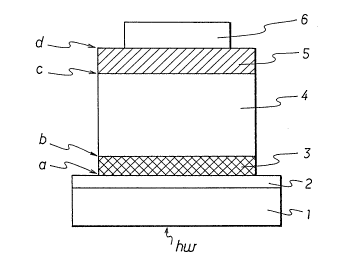
interlayer, can be formed at a junction interface (a) of
a transparent electrode 2 and p-type layer 3 of pin-type
semiconductor device shown in Fig. l; a junction
interface ~b) of p-type layer 3 and i-type layer 4; a
junction interface (c) of i-type layer 4 and n-type
layer 5; a junction interface (d) of n-type layer 5 and a
metal electrode 6; a junction interface (e) of n-type
layer 5 and a transparent electrode 2 of nip-type
semiconductor device shown in Fig. 2; a junction
interface (f) of p-type layer 3 and a metal electrode
6; a junction interface (b) of p-type layer 3 and
i-type layer 4; a junction interface (c) of i-type layer
4 and n-type layer 5; and a p-type or n-type layer. In
the case of a semiconductor device shown in Fig. l, it
is preferable to form the interlayer at a junction
interface (a) of a transparent electrode 2 and p-type
layer 3, particularly junction interface (b) of p-type
layer 3 and i-type layer 4 because such interfaces
locate at the side of light incidence and thereby Voc can
be further improved.
The thickness of the interlayer, which is
formed between semiconductor layers or between a
semiconductor layer and an electrode and comprises a
semiconductor or insulator having higher electrical
resistivity than a semiconductor layer which adjoins the
interlayer, is 10 to 500 A, preferably 10 to 200 A, more
preferably 10 to 100 A. When the thickness of the
interlayer is less than 10 A, the improvement of Voc is a
~ : -
1 32 1 660
-- 8little, and on the other hand when it is more than 500 A,
the reduction of curve factor becomes large.
In the semiconductor device of the present
invention, the interlayer can be produced by glow
discharge decomposition method, sputtering method,
thermal CVD method, photo CVD method or the like, using
such a device that has fundamentally pin-type or nip-type
semiconductor layer such as single-type device,
tandem-type device or integrated-type device. In the
present invention, employable semiconductors are not
particularly limited. That is, any semiconductor can be
used as far as it comprises pin-type or nip-type
semiconductor.
A semiconductor device of the present invention
obtained by the above method is preferably used under a
light source of low illuminance such as a fluorescent
lamp in which series resistance does not seriously become
a problem, because the semiconductor device of the
present invention causes the increase of series
resistance and thereby lowers a curve factor, or the
like.
There can be obtained a semiconductor device
having large Voc and electric current under a specific
voltage like the above-mentioned device, in case of
adding to an interlayer a very small amount of dopant to
such an extent that the electric resistivity of the
interlayer does not become smaller than a semiconductor
layer which adjoins the interlayer.
Next, there is explained the second aspect of
the present invention corresponding to Claim 7 mentioned
later.
As an i-type layer constituting amorphous-
containing pin-type or nip-type semiconductor layers
in the present invention, there can be used a layer of
about 2500 to 9000 A in thickness comprising, for
instance, a-SiC:H, a-Si:H, a-SiGe:H, a-Ge:H, a-Si:F:H,
a-SiN:H or a-SiSn:H; or these amorphous semiconductors
doped by B or P. As a p-type layer, there can be used a
.
~ ., j . :
, . .
1 32 1 660
layer of about 80 to 300 A in thickness formed by doping,
for instance, a-SiC:H, ~c-Si:H or a-Si:H with elements of
group IIIa of the Periodic Table which are p-type
dopants. Further, as a n-type layer, there can be used a
layer of about 80 to 3000 A in thickness formed by
doping, for instance, a-Si:H, ~c-Si:H or a SiC:H with
elements of group Va of the Periodic Table which are
n-type dopants. However, an i-type layer, p-type layer
and n-type layer in the present invention are not limited
to the above-mentioned layers.
Among the above-mentioned p-type layers, layers
obtained by doping a-SiC:H or a-Si:H with elements of
group IIIa are preferable because they have small
activation energy and small light absorption loss.
Further, among the above-mentioned n-type layers, layers
obtained by doping a-SC:H, ~c-Si:H or a-Si:H with
elements of group Va are preferable because they have
small activation energy and high conductivity.
In the foregoing explanation, there are
described, as a p-type dopant, elements of group IIIa of
the Periodic Table, i.e. B, A~, Ga, In and T; and, as an
n-type dopant, elements of group Va of the Periodic
Table, i.e. N, P, As, Sb, Te and Po. However, dopants
employable in the present invention are not limited to
those decribed above, and any dopant can be used as far
as it can produce p-type or n-type semiconductor by
doping therewith.
In the pin-type or nip-type semiconductor layer
of the second aspect of the present invention, there is
provided, in at least one of the p-type layer and n-type
layer, a part wherein an amount of dopant in the p-type
layer or n-type layer is lowest at a junction interface
of p/i or n/i and increases gradually toward a junction
interface of p/electrode or n/electrode.
Fig. 3 is a view explaining an embodiment of a
semiconductor device of the present invention. In Fig.
3, on a glass substrate 11 having a transparent electrode
12 there is provided a p-type semiconductor layer 13 in
...
1 32 1 660
-- 10
such a manner that an amount of dopant is least at a
junction interface of p/i. On the p-type semiconductor
layer 13, an i-type semiconductor layer 14, an n-type
semiconductor layer 15 and a rear electrode 16 are formed
in order.
In the semiconductor device of Fig. 3, an
amount of dopant is least at a junction interface of p/i.
However, the semiconductor device can be produced in such
a manner that the distribution of dopant in the p-type
semiconductor layer is uniform and an amount of dopant is
least at a junction interface of n/i in the n-type
semiconductor layer. The semiconductor device can further
be produced in such a manner that an amount of dopant in
both p-type and n-type semiconductor layers is least at
junction interfaces of p/i and n/i respectively. In Fig.
3, light 17 enters from the p-type layer side, but it
might enter from the n-type layer side. The number of
pin-layer is not limited to one, but it might be stacked
to 2 to 5 layers. In that case, layers on the first
pin-layer might also be made in such a manner that an
amount of dopant is least at a junction interface of
i-layer, or might be made of usual pin-layers shown in
Fig. 4. Numeral 18 in Fig. 4 is a usual p-type layer.
An amount of dopant used in the p-type or
n-type layer is usually 0.01 to 5 atm %, but in the
present invention an amount of dopant in the neighborhood
of a junction interface of p/i or n/i (at which an amount
of dopant is least, preferably in the portion of 20 to 30
A from the junction interface, more preferably in the
portion of 100 A from the junction interface is
preferably not more than 0.01 atm %, more preferably not
more than 0.001 atm %. These facts are made clear from a
result of trial manufactures of semiconductor device by
inventors.
The distribution of dopant is required to
increase gradually from the junction interface of p/i or
n/i to the junction interface of p/electrode or
n/electrode. By way of this constitution, the diffusion
:
.
' ~
1 32 1 660
-- 11 --
of dopant into the i-layer is reduced and the interface
between the i-layer and dopant-layer is improved, and
accordingly the open-circuit voltage is increased.
In the present specification, the expression of
"gradual increase" do not mean a natural increase of
dopants caused by the thermal diffusion, but mean
successive or stairs-like increase obtained by adjusting
an amount of dopant. In that case, from a viewpoint of
increasing Voc, it is preferable that components other
than dopant in the p-type or n-type layer do not
substantially change.
Fig. S is a view explaining an embodiment of
the distribution of dopant in a semiconductor device of
the second aspect of the present invention wherein
p-type, i-type and n-type layers comprise a-SiC:H, a-Si:~
and a-Si:H, respectively. In Fig. 5, A is a graph
showing a distribution of p-type dopant in a p-type
semiconductor layer, B is a graph showing a distribution
of n-type dopant in an n-type semiconductor layer, and C
and D are graphs showing distributions of p-type dopant
and n-type dopant in a conventional semiconductor device.
Fig. 5 only shows an preferable example of the
distribution of dopant in the p-type or n-type layer,
and the condition of distribution is not limited to that
shown in Fig. 5. In other words, it is only required
that the dopant content of at least one conductivity
layer is minimized at a junction interface of p/i or n/i.
In case of producing a semiconductor device of
the present invention using a-SiC:H as a doped layer, an
insulating layer of a-SiC:~ which is not doped exists at
a junction interface of p/i or n/i. But, in the present
invention, such a construction is employable.
Electrodes used in the present invention are
not particularly limited, but there can be employed a
transparent electrode, metal electrode, silicide
electrode, or a laminated electrode obtained from these
materials, which are usually used in producing solar
cells.
-
~ : '
- " :::
1321660
- 12
As an apparatus of producing a semiconductor in
the present invention, there can be employed a
parallel-plate capacitively-coupled type plasma CVD
apparatus, an inductively-coupled type plasma CVD
apparatus, thermal CVD apparatus, ECR plasma CVD
apparatus, photo CVD appartus, excited species CVD
appartus, and the like. But employable apparatuses are
not limited to these ones. A method of producing a
semiconductor in the present invention and material used
therein are not particularly limited.
A pin construction or nip construction in
the present invention is one generally used in
photovoltaic devices or photodiodes comprising amorphous
semiconductor.
Next, there is explained the third aspect of
the present invention corresponding to Claim 16 mentioned
later.
A semiconductor device in the third aspect of
the present invention comprises a nip-type or pin-type
amorphous-containing semiconductor layer, wherein at
least one semiconductor layer tI) being the same
conductivity type as the adjacent semiconductor (II) and
having higher impurity density is/are interposed between
the semiconductor layer tII) and an electrode.
In a pin-type or nip-type amorphous-containing
semiconductor used in the third aspect of the present
invention, as a i-type semiconductor layer, there can be
used a layer of about 200 to 9000 A in thickness
comprising, for example, a-Si:H, a-SiGe:H, a-Ge:H,
a-Si:F:H, a-SiN:H or a-SiSn:H, a-SiC:H, or these
amorphous semiconductors doped by a very small amound of
B or P. As a p-type semiconductor layer, there can be
used a layer of about 80 to 300 A in thickness formed by
doping, for instance, a-SiC:H, ~c-Si:H or a-Si:H with
elements of group IIIa of the Periodic Table. Further,
as a n-type semiconductor layer, there can be used a
layer of about 80 to 300 A in thickness formed by doping,
for instance, a-Si:H, ~c-Si:H or a-SiC:H with elements of
,
.
,
1 32 1 660
group Va of the Periodic Table. However, an i-type,
p-type and n-type semiconductor layer in the present
invention are not limited to the above-mentioned layers.
Among the above-mentioned p-type semiconductor
layers, layers obtained by doping a-SiC:H or a-Si:H with
elements of group IIIa are preferable because they have
small activation energy to generate holes which contribute
to conductivity of semiconductors, and small light
absorption loss. Further, among the above-mentioned
n-type semiconductor layers, layers obtained by doping
a-SiC:H, ~c-Si:H or a-Si:H with elements of group Va are
preferable because they have small activation energy to
generate electrons which contribute to conductive of
semiconductors and high conductivity. However, materials
used in the above i-type, p-type and n-type semiconductor
layers are not limited to those described above.
In the foregoing explanation, there are
described as a p-type dopant, elements of group IIIa of
the Periodic Table, i.e. B, Al, Ga, In and Tl; and, as an
n-type dopant, elements of group Va of the Periodic Table,
i.e. N, P, As, Sb, Te and Po. However, dopants
employable in the present invention are not limited to
those described above, and any dopants can be used as far
as they can produce p-type or n-type semiconductor by
doping therewith.
In the present invention, the impurity density
of p-type and/or n-type layer, interposed between a
p-type semiconductor layer and an electrode at the side
of p-type semiconductor layer and/or between n-type
semiconductor layer and an electrode at the side of
n-type semiconductor layer, is more than two times,
preferably more than four times of usual impurity
density. The upper limit of the impurity density is not
particularly limited, but is usually adjusted to not more
than 10 atm ~. The thickness of the high density
semiconductor layers is 10 to 300 A, preferably 30 to 150
A.
Now, there are explained Examples and
1321660
Comparative Examples with respect to the first, second
and third aspects of the present invention, wherein
Examples 1 to 11 and Comparative Example 1 correspond to
the first aspect of the present invention, Example 12
and Comparative Example 2 correspond to the second aspect
of the present invention and Example 13 and Comparative
Example 3 correspond to the third aspect of the present
invention.
Examples 1 to 8
A glass substrate was obtained by depositing
SnO2 film of 0.1 ~m thick on a glass plate of 1.1 mm
thick by means of thermal CVD method.
The obtained glass substrate was heated up to
240C to form thereon a p-type a-SiC:H layer of 150 A in
thickness using a parallel-plate capacitively-coupled
type plasma CVD apparatus, whereinto 50 sccm of mixed gas
of three types of 1000 ppm diborane, i.e. (A) diborane
diluted with monosilane, tB) diborane diluted with
methane and (C) diborane diluted with hydrogen (a flow
ratio of (A), (B) and (C) is 1 : 3 : 1) was introduced
and glow discharge decomposition was carried out with
rf frequency of 13.56 MHz and rf power of 30 W.
About 20 atm % of carbon was contained in the
obtained p-type a-SiC:H layer. The conductivity of the
a-SiC:H layer was about 10 7 (Q-cm) 1.
After exhausting a residual mixed gas, a mixed
gas consisting of 20 sccm of monosilane and 30 sccm of
methane was introduced into the apparatus to form,
without using doping gas, an interlayer comprising a-SiC
of which thickness is shown in Table 1.
Next, after exhausting a residual mixed gas, 50
sccm of monosilane gas was introduced and glow discharge
decomposition was carried out with rf frequency of 13.56
MHz and rf power of 30 W in the same manner as described
above to form i-type a-Si:H layer of 7000 A in thickness.
Then, glow discharge decomposition was carried out with
rf having the same power as mentioned above, using 100
1 32 1 660
- 15
sccm of lO00 ppm phosphine gas diluted with 20 scc~ of
monosilane, and hydrogen, to form n-type a-Si:H film of
300 A in thickness.
Next, A~ was evaporated as a rear electrode
using resistive-heating type vacuum evaporation apparatus
to make a photoelectric converter.
In accordance with the same manner as described
above, five photoelectric converters were further made.
Voc and curve factor of six photoelectric converters were
measured under a fluorescent lamp at an illuminance of
200 lux. The results are summarised in Table 1.
: :
- 1321660
-- 16
~ G) 0~ u~
~ ~ ~ ~ o c~ ~r
~ ~ t~
O
U
E a) ~ ~ a
~^ ._, 1 . . . . . . . .
dP C ~ ~ ~ ~ 3~ ~` ~ o 1`
_ ~ ~ I` I` I` ~ I~
c~ E
,.
E ~ ~ o ~D o ~ I` ~ a~
~ ........
X ~ u~ n u~
r~
a) u~ u~
~ O et~~01~ N O OD 1` U~ O
l.l ~ ~ D ~D
O O ~ . , , . , . . . .
~ ~ (~S O O O O O O O O O
_~ ~15 ~ ~
O ~
E o ~ ~ D ~ o
._~_ ~ ~ D ~D
~ :~ C ~ . . . . . . . . .
~_ '~ ~ o o o o o o o o o ,.
~ :'
c E ~ ~ ~
O rl ~ ~D ~ ~D 1` 1` ~D ~D U:) ~D
X ~ . . . . . . . . .
~ ~ o o o o o o o o o
u~ ~
c~ oooooooo
~C c ~0~ ~ ~ o
r~ ~ ~ _ ~1 -~ ~ N :
E-~ O -~
~ 0 . ~
. . . . . . . . E ~
XXXXXXXX oX
~)
. ~ ~
' :
1321660
- 17
Exmaples 9 to 11
The procedure of Example 4 was repeated except
that interlayers were formed at a junction interface of
a transparent electrode ana a p-type layer (hereinafter
referred to as TE/P) (Example 9); at a junction interface
of an i-type layer and an n-type layer (hereinafter
referred to as i/n) (Example 10); and at a junction
interface of an n-type layer and AQ electrode
(hereinafter referred to as n/AQ) (Example 11). Voc and
curve factor were measured like in Examples 1 to 8. The
results are summarized in Table 2.
.
1 ~2 1 660
-- 18
~ N ~ 3
fl g I` I` U~ I~
o e
~_ e a) ~ O 1
d C ~ ~i N 0 ~
_ ~ g 1~ D
e
ea, a~o~ N
X ~ er U~ ~ ~
a) u~ ,''
a) ~ '9 ~D ~ O "
N ~ ~ g O O O O
R g ~
E~ ~ ~ O In N r~) O
. ~ C ~ ~ O ~D
~)_ ~ ~ O O O O '
o
~ ~ In
OX ~ ~ 9 N
~ 000 O
S::~ .
O (~ P. ~1
. ~1 ~ ~ ~ l
OoC E~
a~o~ .~
X ~ ~ o ~
1 32 1 660
-- 19
Comparative Example 1
A glass substrate was obtained by depositing
SnO2 film of 0.1 ~m thick on a glass plate of 1.1 mm
thick by means of thermal CVD method.
The obtained glass substrate was heated up to
240C to form thereon a p-type a-SiC:H layer of 150 A in
thickness using a parallel-plate capacitively-coupled
type plasma CVD apparatus, whereinto 50 sccm of mixed gas
of three types of 1000 ppm diborane, i.e. (A) diborane
diluted with monosilane, (B) diborane diluted with
methane and (C) diborane diluted with hydrogen (a flow
ratio of (A), (B) and !C) is 1 : 3 : 1) was introduced
and glow discharge decomposition was carried out with rf
frequency of 13.56 MHz and rf power of 30 W.
About 20 atom % of carbon was contained in the
obtained p-type a-SiC:H layer. The conductivity of the
a-SiC:H layer was about 10 7 (~-cm)
Next, after exhausting a residual mixed gas, 50
sccm of monosilane gas was introduced and glow discharge
decomposition was carried out with rf frequency of 13.56
MHz and rf power of 30 W in the same manner as described
above to form i-type a-Si:H layer of 7000 A in thickness.
Then, glow discharge decomposition was carried out with
rf having the same power as mentioned above, using 100
25 sccm of 1000 ppm phosphine gas diluted with 20 sccm of
monosilane, and hydrogen, to form n-type a-Si:H film of
300 A in thickness.
Next, A~ was evaporated as a rear electrode
using resistive-heating type vacuum evaporation apparatus
to make a photoelectric converter.
In accordance with the same manner as described
above, five photoelectric converters were further made.
Voc and curve factor of six photoelectric converters were
measured under a fluorescent lamp at an illuminance of
35 200 lux. Voc was 0.60 to 0.62 V (0.606 V in average),
and curve factor was 74.5 %. These results are
summarised in Tables 1 and 2.
: . ,. ~- .. , :-
: - : -
'' ~
1321660
- 20
Example 12 and Comparative Example 2
A solar cell having a construction shown in
~- Fig. 3 was made as an experiment.
SnO2 of 800 A in thickness, as a trasparent
electrode, was deposited on a glass to obtain a
substrate.
p-type a-SiC:H film of 150 A in thickness was
accumulated on the substrate by means of plasma CVD
method. Using SiH4, CH4 and B2H6 (diluted to 1000 ppm
with hydrogen) as material gas for p-type a-SiC:H, 70 A
of SiH4, CH4 and B2H6 at 10 sccm, 30 sccm and 200 sccm
respectively. Then, continuing glow discharge, residuary
80 A of a-SiC:H was accumulated while gradually
decreasing an amount of B2H6. The flow rate of B2H6 when
the deposition of p-layer was completed was 0 sccm.
i-type a-Si:H layer of 7000 A in thickness was deposited
by means of glow discharge decomposition. Then, n-type
~c-Si:H layer of 300 A in thickness was deposited by
means of glow discharge decomposition, using a mixed gas
of 20 sccm of SiH4 and 100 sccm of 1000 ppm PH3 diluted
with H2. A~ of 1000 A in thickness was vacuum evaporated
thereon as a rear metal electrode to make 1 cm device.
The amount of dopant in the p-type layer when
flowing a constant volume of B2H6 was 2 atm %.
For comparison's sake, solar cells of
conventional type were made by the same manner as
described above, except that p-type a-SiC:H of 150 A in
thickness was deposited under the above constant flow
rate.
V-I characteristic of the obtained two kinds of
solar cells was measured under fluorescent at a
illuminace of 200 lux. The results are shown in Fig. 6.
The open-circuit voltage of the solar cell of
Comparative Example 2 was about 0.6 V. On the other
hand, that of the solar cell of Example 12 was 0.70 V.
It was observed that the electric current and FF (Curve
Fill Factor) were improved a little.
~.
1 321 660
Example 13
Fig. 7 shows Example 13 of a semiconductor
device of the present invention wherein the semiconductor
layer is pin-type of triple layer construction. In Fig.
7, there is formed a p-type semiconductor layer 23 of
high impurity density between an electrode 22 at the side
of a p-type semiconductor layer 24. The semiconductor
layer 23 is attached on the top surface of the electrode
22 and at the bottom surface of the p-type semiconductor
layer 24.
In Example 13, the construction of pin-type
semiconductor layer is similar to that generally employed
in photovoltaic devices, photodiodes, or the like which
comprise amorphous semiconductor.
Next, a method of producing a semiconductor
device of Example 13 is explained.
First of all, an electrode 22 at the side of a
p-layer, which is a transparent electrode, is deposited
on a grass plate 21 by means of sputtering method.
SnO2 is used as a material of a transparent electrode.
The thickness of the electrode is 5000 A.
Next, on the electrode 22 at the side of
p-layer, there is formed a p-type semiconductor layer
23 of high impurity density by doping SiC:H with B by
means of plasma CVD method. In forming the p-type
semiconductor layer 23 of high impurity density, SiH4,
CH4 and B2H6/H2 (a concentration of B2H6 is 1000 ppm) are
used. The flow rate is 10 sccm, 30 sccm and 200 sccm,
respectively. The thickness of the obtained p-type
semiconductor layer 23 of high density is 100 A, and the
impurity density thereof is 4 %.
Next, on the semiconductor layer 23, there is
formed a p-type semiconductor layer 24 by doping SiC:H
with B by means of plasma CVD method in the same manner
35 as described above, except that the flow rate of B2H6/H2 ~ -
is changed to 50 sccm. The thickness of the obtained
p-type semiconductor layer 24 is 100 A, and the impurity
density thereof is 1 %.
:~ -
. .
1 321 660
- 22
Thereafter, an i-type semiconductor layer 5
comprising a-Si:H is formed on the p-type semiconductor
layer 24 by means of glow discharge decomposition using
SiH4 as a material gas. The thickness of obtained i-type
semiconductor layer 25 is 5000 A.
Next, on the i-type semiconductor layer 25,
there is formed an n-type semiconductor layer 26 by means
of glow discharge decomposition using SiH4 and PH3/H2 (a
density of PH3 is 1000 ppm). The flow rates of SiH4 and
PH3/H2 are 10 sccm and 50 sccm, respectively. The
thickness of obtained n-type semiconductor layer 6 is 300
A, and the impurity density thereof is 0.5 %.
Further, an electrode 27 at the side of the
n-type semiconductor layer is formed on the n-type
semiconductor layer 26 by vacuum evaporated Ag. The
thickness of formed electrode 27 is 1000 A.
The area of a semiconductor device prepared in
accordance with the above method is about 1 cm2, but it
is possible to prepare those of 1 to 500 cm2 in area.
However, the area of the device is not limited in the
present invention.
In the semiconductor device of Example 13,
light enters along a direction of arrows shown in Fig. 7
to generate pairs of electrons and holes in the
25 semiconductor layers 23, 24, 25 and 26 like in the
semiconductor device of Fig. 9, and to generate positive
charge at the electrode 22 at the side of p-layer and
negative charge at the electrode at the side of n-layer.
In the present Example, since the electrode 22 at the side
of p-layer contacts with the p-type semiconductor layer 23
of high density, the contact resistance between them is
remarkably decreased. Further, the light absorption loss
in the impurity-containing portion do not increase
because the p-type semiconductor layer 23 of high density
is thin.
Comparative Example 3
The procedure of Example 13 was repeated except
1 32 1 660
- 23
that there was formed a semiconductor having the same
quality of the material as p-type semiconductor layer 24
and a thickness of 100 A, by means of the same method of
forming the p-type semiconductor layer 4 as in Example
13, instead of the p-type semiconductor layer 23 of high
density.
With respect to semiconductor devices of
Example 13 and Comparative Example 3, V-I characteristic
was measured under a solar simulator of 100 mW/cm2. The
results are shown in Fig. 8.
According to V-I characteristic shown in Fig.
8, full factor (F.F.) was calculated by the following
formula:
Maximum output
- x 100
Short current x Open-circuit voltage
The fill factor of Example 13 was about 70 ~, while that
of Comparative Example 3 was about 60 %.
In Example 13, the p-type semiconductor layer
23 of high impurity density was interposed between the
electrode 22 at the side of p-type layer and the p-type
semiconductor layer 24. However, the same effect can be
obtained when interposing an n-type semiconductor layer
of high impurity density between the n-type semiconductor
layer and the electrode 27 at the side of n-layer.
Further, in Example 13, light enters from the
electrode at the side of p-layer. But, light might enter
from the electrode 27 at the side of n-layer by making
the electrode 27 transparent.
Though, in Example 13, only a set of the
p-type, i-type and n-type semiconductor layers are
formed, the number of sets might be 6 to 15, and further
the accumulation order might be such that n-type, i-type
and p-type layers are formed in order from a substrate in
Fig. 7.
SnO2 was used as a material of the transparent
electrode in Example 13, but other material such as ITO
is employable. Further, Ag was used as a material of the
: , , .,. '-' ' :. :: ~: .
.., ~ :
,,
:
1 32 1 660
- 24
electrode 27 at the side of n-layer, but there can be used
other conductive metal such as A~ or Au; conductor such
as silicide which is a compound of silicon and other
metal; laminated electrode of these conductive metal and
conductor, or the like.
In Example 13, the material of the
semiconductor layer 23 of high impurity density was the
same as p-type semiconductor layer 24, but it might be
different from the material of p-type semiconductor layer
24 as far as it is a p-type semiconductor. For example,
Si:H is employable instead of SiC:H used in Example 13.
In that case, not only B used in Example 13 but also
other impurity might be used. Of course, only the kind
material of impurity can be changed to another material,
employing the same type of semiconductor layer. This
modification can also be applied to an n-type
semiconductor layer of high impurity density and n-type
semiconductor layer.
The impurity density in Example 13 changed
discontinuously from the p-type semiconductor layer 24 to
the p-type semiconductor layer 23 of high impurity
density. However, it might gradually increase from the
p-type (or n-type) semiconductor layer to the p-type (or
n-type) semiconductor layer of high impurity density.
As a method of producing each layer of the
semiconductor device in Example 13, sputtering method,
vacuum evaporation method, plasma CVD method, or the like
were used. But, any other method is employable as far as
a thin film can be obtained by the method. A CVD
apparatus employable in the present invention includes,
for instance, parallel-plate capacitively-coupled type
plasma CVD apparatus, conductively-coupled type plasma
CVD apparatus, thermal CVD apparatus, ECR plasma CVD
apparatus, photo CVD apparatus, exited species CVD
apparatus.
The materials usable to form each layer are not
limited to those employed in Example 13.
As is described in detail hereinbefore, the
,,
~ '
1 321 660
- 25
semiconductor device according to the first and second
aspects of the present invention has larger Voc and
electric current (working current) at a specific voltage
than conventional devices, thereby it can preferably be
used in consumer-use solar cells, particularly in such
solar cells that are equipped with electrical and
electric equipment used under low-illumination light
source such as fluorescent lamp.
Further, the semiconductor device according to
the third aspect of the present invention can not only
reduce the contact resistance between a p-type
semiconductor layer and an electrode at the side of the
p-type layer and/or between an n-type .semiconductor layer
and an electrode at the side of the n-type layer, but
also maintain the light absorption loss small, whereby
photoelectric conversion efficiency can be improved in
comparison with conventional semiconductor devices.
: - .
. ~ :
: