Note: Descriptions are shown in the official language in which they were submitted.
1 321 661
WAFER HANDLING SYSTEM
Technical Field
This invention pertains to the automatic handling
of semiconductor wafers in a lithographic process.
Background Art
Conventionally, semiconductor wafers are coated
with photoresist material and exposed to radiation from a
mercury lamp in order to apply electrical circuits
thereon. This process is repeated a number of times,
typically in a projection mask alignment and exposure
system. It is extremely important that a wafer be
precisely oriented for each exposure in order to insure
correct registration of each successive image. The usual
methods of transporting a wafer within such a system have
been by means of belts and air tracks. However, these
methods have not provided sufficiently positive control.
As a result, wafers have tended to slide and bounce,
thereby generating particles which, upon landing on the
wafer could damage the micro circuits being printed.
Accordingly, it is an object of this invention to
increase the control exercised over each wafer while, at
the same time, precisely aligning each wafer with a
:. ~
1321661
minimum of handling. The manner in which this is
achieved will be apparent from the following desGription
and appended claims.
Disclosure of Invention
A randomly oriented semiconductor wafer contained
in an input cassette is automatically removed from the
cassette and, in one revolution, is Gharacterized in X,
Y, and 0 with respect to a spin axis. It is rotated to a
predetermined 0 position and is transferred onto a
transport stage that has been pre-positioned in X and Y,
in accordance with the offsets determined during
rotation.
Brief Description of Drawings
FIG. 1 is a partially schematic plan view which
illustrates the movement of a wafer in accordance with
the invention;
FIG. 2 is an elevational cross-section through
the pre-aligner of the invention;
FIG. 3 is an enlarged detail, partially in cross-
section, of the input shuttle of the invention;
FIG. 4 is an elevational view of the wafer lifter
of the invention with portions of the wafer and wafer
~ : : .
~ .
.
1 3~1 661
chuck in cross-section;
FIG. 5 is an elevation of the output shuttle of
the invention; and
FIG. 6 is a right end view of the shuttle of FIG.
5.
Best Mode for Carrying out the Invention
Illustrated in FIG. 1 are portions of the
structure 10 of an automated lithographic instrument for
the production of semiconductor wafers. An input
cassette 12 of conventional construction holds a
plurality of wafers 14 in random orientation. As will be
apparent from the plan view of FIG. 1, the wafers 14
within the cassette 12 are horlzontally positioned. The
cassette 12 is lowered by means of a lead screw (not
shown) in fixed increments to successively deposit each
of the wafers 14 onto a load shuttle 16. The load
shuttle 16 includes a conventional hook shaped portion
having a vacuum groove for securely retaining the wafer
14.
The load shuttle 16 is connected for
reciprocation along a "loading" air bar 18 which is of
conventional construction, i.e., a square tube 20 movable
along and spaced from a bar 22 by means of air pressure.
Each of the wafers 14 is transported in turn by the load
. ~ ~
1321661
-- 4
shuttle 16 to a position designated 14a above a pre-
aligner.
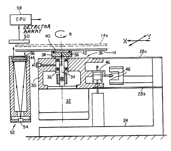
The pre-aligner, which is illustrated in FIG. 2,
comprises a base member 24 from whiGh a motor assembly 26
is suspended by a pair of leaf flexures 28a, 28b. The
motor assembly 26 comprises a support housing 30 to which
is secured a dc motor 32. The motor shaft 34 extends
upwardly through bearings 36 to a spinner 38 which
defines a vacuum chamber 40 connected by a channel 42 to
a vacuum source 44. The vertical position of the motor
assembly 26 is controlled by an air pot 46 and limit
stops 48. The air pot 46 forces the motor assembly 26
upward so that the spinner 38 engages the underside of
the wafer at 14a and vacuum is applied to chamber 40.
The vacuum on load shuttle 16 releases and the load
shuttle is retracted along the air bar 18 into its
initial position to extraGt the next wafer. The motor
assembly 26 is then retracted by the air pot 46 to the
position indicated in FIG. 2.
Positioned above the edge of the wafer 14 is a
detector array 50. This may be a commercially available
detector such as the Fairchild CCD 143 comprising a
linear array of light detecting elements. Positioned
below the wafer and the array 50 is an illumination
system 52 comprising a light source 54 and collimating
lens 56. As will be apparent from FIG. 2, a portion of
.
1 321 661
the light from the illuminating system 52 is blocked by
the wafer 14 from reaGhing the detector array 50. If the
Genter of the wafer 14 is exaGtly aligned with the axis
of rotation of the spinner 38, the amount of light
received by the deteGtor array 50 remains Gonstant
throughout a revolution of the wafer (exGept for that
passed by the notGh or flat described below). If,
however, the wafer is offset in X or Y (mutually
orthogonal axes in the plane of the wafer), the output
from the detector array 50 will be cyGliGally variable.
This output is supplied to a central processing unit
(CPU) 58 which is programmed to determine the X and Y
offsets.
The manufacturers of semiGonductor wafers
incorporate some type of angular, or "0" indicia on each
wafer to indicate the direGtion of crystal growth. This
is required because it is important for chip produGers to
properly position cirGuits in accordance with crystal
orientation. The wafer shown in position 14a of FIG. 1
carries a small notch 60 as a 0 indicia. Flats are also
widely used for this purpose. In any event, during the
one rotation of the wafer 14, the 0 indicia will be
readily noted by the presence of an extra light pulse at
detector 50 which passes a resulting signal to the
central processing unit 58. It is then a simple matter
for the central processing unit 58 to command the motor
. ~ .
~ , ,
1 321 661
-- 6
32 to stop with the 0 indicator in a desired
predetermined position.
The X and Y offsets computed by the central
processing unit 58 are employed to pre-position a vacuum
chuck 62 which forms a portion of a transport stage which
will be employed to expose the wafer to a circuit
pattern. Upon completion of pre-alignment, the spinner
once again raises the wafer to the 14a position where it
is engaged by an input shuttle 64 mounted for translation
along the X direction on an air bar 66. As will be
apparent from FIG. 3, the input shuttle assembly 64
includes a shuttle arm 68 having the usual C-shaped
vacuum groove 70 for securely holding a wafer 14. It is
mounted on a shaft 72 for 90 pivotal rotation on
bearings 74 under control of a stepping motor 76 through
gear box 78.
After acquiring the wafer 14, the input shuttle
68 moves in the X direction to the left as viewed in
FIG. 1 and, at the same time, it is rotated downwardly
through 90 to position the wafer 14 in a vertical plane
in order that it may be acquired by the pre-positioned
vacuum chuck 62 of the transport stage.
Vacuum chuck 62 acquires the wafer by the
mechanism shown in FIG. 4. This comprises a head 80
carrying rubber vacuum cups 82 mounted on flexures 84
under the control of an air pot 86. The air pot 86
- 1321661
-- 7
forces the head 80 through the central opening in chuck
62 permitting the vacuum cups 82 to engage the wafer 14.
The assembly is then retracted to place the wafer 14 on
the vacuum chuck 62 where it is retained by the vacuum
grooves 88. As explained above, the vacuum chuck 62 has
been pre-positioned to compensate for the initial X and Y
displacements seen by detector 50. This pre-positioning
may be accomplished by means of a planar force motor such
as those described, for example, in the following United
States Patents:
4,485,339 of Trost for "Electro-Magnetic
Alignment Device";
4,506,205 of Trost and Galburt for "Electro-
Magnetic Alignment Apparatus"; and
4,507,597 of Trost for "Electro-Magnetic
Alignment Assemblies".
SuGh motors provide very accurate control of
rotational position. Accordingly, they are employed to
make very fine adjustments in 0 as well as X and Y.
When the wafer 14 has been accurately positioned
on the chuck 62 it is advanced to the exposure stage
(which does not form a part of this invention). After
exposure, the wafer is unloaded by the output shuttle
assembly illustrated in FIGS. 5 and 6. The output
shuttle 90 engages the wafer 14 as shown in FIG. 5 and is
then retracted to the dotted line position. It also
~ :.: . : :
` 1 32 1 66 1
rotates the wafer 90 to a horizontal position from which
it is inserted into the output cassette 92. As this
cassette is located on a different level from that of the
input cassette 12, it is illustrated in FIG. 1 by dotted
lines.
It will be noted that the system described herein
is fully automatic and requires operator assistance only
for loading and unloading of the cassettes. It
automatically and precisely orients each wafer prior to
exposure. It will also be noted that a number of
variations and modifications may be made in this
invention without departing from its spirit and scope.
Accordingly, the foregoing description is to be construed
as illustrative only, rather than limiting. This
invention is limited only by the scope of the following
claims.
,
'' ~ .