Note: Descriptions are shown in the official language in which they were submitted.
MI-3788
1'32~7~
SYNTHETIC IMAGING TECHNIQUE
BACKGROUND OF THE INVENTION
. . .. .. . .
One type of data storage media utilize optical
disks. In this type of data storage photolithographic
techniques are utilized to form circular or spiral patterns
on glass disks in much the same way as integrated circuits
are formed on silicon wafers. The patterns consist of lines
and spaces on which data may be permanently or temporarily
stored. In the latter case the lines and or spaces may be
formed of sensitive materi~l on which lasers may be used to
read, write or erase and rewrite. More conventional read,
write and rewrite techniques such as magnetic read-write
heads may also be used. A very important feature of such
memory disks is the density at which data may be stored
thereon. The storage density is a function of the closeness
at which discrete lines;and spaces are formed on the disks~
'~
' .
3 2 1 7 1 7
- 2 - MI~3788
BRIEF SUMMARY OF THE INVENTION
In the present invention an illumination source
projects light through a mask positioned at the object plane
of an imaging optical system such as a projection mask
aligner. In a typical projection mask aligner of the type
disclosed in U.S. Patent Nos. 3,7~8,015; 4,293,186 and
4,011,011 the pattern of the mask would be projected or
imaged on the target, e.g,, a wafer or optical disk without
change in the image. The number of lines and spaces, on the
mask pattern would be reproduced on the optical disk without
a change in the period. In normal practice the newest model
of the Micralign Model 600 projection mask aligners of the
type manufactured by the Perkin-Elmer Corporation o~ Norwalk,
Connecticut is capable of forming high contrast (modulation)
images of repetitive patterns such as groups of lines and
spaces, concentric circles or spirals with the same mask (~m)
and image ~i) period as small as
~ m = ~ /NA = 2.2 um
where the Model 6Q0 has a numerical aperatue of NA =
0.167. The wave length is~ = 365 nm. the image can be used
to expose a light sensitive coating on a glass disk to meet
the specific re~uirements of an optical disk. This mall
period approaches the practical limits of photolithography.
Repetitive patterns of smaller period, 1.7 to 1.3 um, can be
imaged only under ideal conditions because of the low contast
image. In addition, the depth of~focus is very llmited.
.
:
::
.
~32~717
- 3 - MI-3788
In the present invention the image differs
significantly from the mask pattern: the image period is one
half the mask period, iOe., the previous 2.2 um period is
imaged as a high contrast 1.1 um period image. In addition
this image has a large depth of focusO To carry out this
invention means are provided within the optics of the
projection system to block out all orders of liyht diffracted
by the mask pattern except for the desired positive and
negative first orders.
In a practical embodiment the invention comprises an
off-axis system comprising a concave and convex mirror
arranged to have their centers of curvature coincident or
nearly on the optical axis. An illumination source projects
light of controlled coherence through a mask disposed at one
conjugate to image the pattern at the other conjugate point
of the system. Obscuration means are provided at the convex
mirror (system pupil~to block all orders of light diffracted
by the mask pattern except the two first orders from reaching
the target, e.g., the optical disk. This results in an image
~0 of the mask pattern having half its period. It should be
remembered that in the system described the mask and wafer
must be scanned past the annular area of good correction as
described, e.g., in U.S. Patent No. 4,011,011 in order to
fully expose the optical disk.
~5 In another embodiment the optical system is purely
refractive, e.g., as in step and repeat projection mask
aligner. Here again, obscuration means are used to block all
light diffractd by the mask pattern except the first order.
..
. :
-
.
13~71~
- 4 - MI-3788
In both cases careful selection of parameters are
necessary for optimum performance, e.g., illumination,
spatial and spectral coherence, object mask pattern and
optical imaging system stop should be carefully selected in
a coordinated manner. Unequal lines and spaces may be made
by the appropriate exposure selection.
BRIEF DESCRIPTION OF THE DRAW:CNGS
Fig. 1 illustrates in schematic form a first
embodiment of the present invention utilizing an off axis
optical system; and
Fig. 2 illustrates in schematic form another
embodiment of the present invention utilizing an on axis
optical system.
DESCRIPTI ~ON
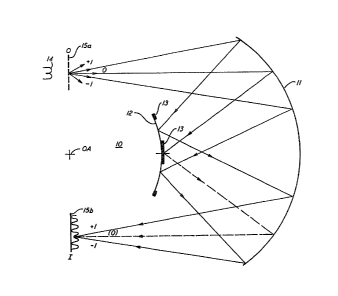
Referr;ing to Fig. 1 there is shown an of axis
afocal optical system 10 comprising concave mirror 11 and
convex mirror 12. Concave mirror 11 and convex mirror 12 are
arranged so that their centers of curvature are nearly
coincident on the optical axis of the system. The mirror
~0 suraces o concave mirror 11 and convex mirror 12 face each
other. The radius of curvature of convex mirror 12 is
smaller than that of concave mirror 10 so that rays of light
from object point O are reflected from concave mirror 11 to
convex mirror 12 and thence to concave mirror 11 and
'
.
.
~32~7~7
- 5 - MI-3788
therefrom to image point I. This arrangement produces a well
corrected image of the object within an annular ring
concentric to the optical axis which is highly useful in the
microlithography art as described in the above mentioned
patents. The term "nearly coincident~ is used inasmuch as it
has been shown that if the centers of curvature are permitted
to deviate a little from coincidence, the width of the ring
of well corrected imagery is increased and is still within
acceptable microlithography standards.
By placing obscurations 13 as shown at or on the
convex mirrox 12 an image of a mask 15a patterned wi~h
concentric or spiral circles having a period A placed at the
object point and properly illuminated by a source 14 will
project an image of the pattern to the image point I having a
period ~ A. An optical disk 15b placed at the image point
thus would be exposed to a pattern with lines and spaces half
the period of those on the mask. Appropriate processing,
e.,q. developing and etching will then provide an optical
disk having a storage capacity four times that normally
possible.
The obscurations Eunction as a spatial filter and
block all orders of diffracted light through the mask except
the two ~irst orders, i.e., the 2ero order and second and
greater orders of light are blocked. This results in the
phenomena of halving the period of the lines and spaces
projected onto a target disposed at the image plane I. Thus,
on processing a photoresist coated ~lass disk results in an
optical disk with double the number of lines and spaces
possible through conventional techniques and, thus, allowing
up to four times the storage capaci~y.
~32~7~7
-- 6 - MI--3788
Table 1 lists the basic system parameters referred
to the image. The desired diffracted orders are txansmitted
through ~he unobstructed pupil between Nl and N2.
TABLE 1
S System Variables
Wavelength of light : 1
Image system numerical aper~ure No
Source numerical aperture : Ns = ~5 No
. Central pupil stop numerical aperture : Nl ~ ~1 No
. Outer pupil stop numerlcal aperture N2 = ~2 No
The source coherence is ~ s ; ~1 and '2 are constants of
proportion where oc ~5 ~ ~1 and 0~ ~ (G'2 ~ ~'1)
The mask period is ~ m
. The image period is 1 = ~ n
lS Table 2 gives- the basic relationships for this
imaging technique. The relationships must hold for all
variables i.e., over all image period ranges and wavelengths
used.
:
:132~7:i7
- 7 - MI-3788
TABLE 2
c Ns ~N~ m - Ns )
( ~ m+ Ns J~ N2 ~ (2 A~m ~ Ns) ~ No
Fig. 2 illustrates an on axis refractive optical
system embodying the concept of the reflective off axis
optical system of Fig. 1.
The optical system of Fig. 2 comprises a spectrally
filtered light source 16 of controlled area ~or a laser),
collimating lens 17, a mask 18 disposed at the object plane
of the system, imaging lenses 19 and 20, and an optical disk
21 disposed at the image plane of the system. The optical
disk 21 is coated with a light sensitive material. A spatial
filter 22 is disposed between lenses 19 and 20 at the ~pupil)
focal plane of lens 19. The spatial filter 22 is essentially
a stop having an opaque center portion 22a and an opaque
outer annular portion 22b which together form an annular
opening 22c.
The mask 18 is patterned the same as mask 15a of the
system of Fig. 1, i.e., with concentric or spiral rings
having period ~m~ The pattern may be composed o~
transparent spaces and opaque lines or of alternating phase
differences in an all transparent phase mask or a
combination.
~321~7
-- 8 -- MI--3788
Upon illumination of the mask 18 its pattern is
imaged at the image plane onto optical disk 21. As in the
case of the system of Fig. 1 the imaged pattern has a period
which is one half that of the mask pattern~ Thus, after
appropriate processing, e.g., developing and etching the
memory capacity of the optical disk 21 is up to four times
that ordinarily expected from the mask 18.
Other modifications of the invention are possible in
light of the above description which should not be
interpreted as placing limitations on the invention beyond
those set forth in the Claims which follow: