Note: Descriptions are shown in the official language in which they were submitted.
1321 83~
.
Description
TWO SQUARE MEMORY CELLS HAVING H:CGHLY CONDUCTIVE
WORD LINES
Technical Field
.
This invention relates to integrated semicon-
ductor memory circuits and more particularly to a
memory with a very high density of cells, each of
which employs means for storing a binary digit of
information in a trench or groovP formed in a
semiconductor substrate.
Background Art
Integrated semiconductor memory circuits,
particularly those employing cells which include
essentially a storage capacitor and a switch have
achieved high memory cell densities. one of the
simplest circuits for providing a small dynamic
memory cell is described in commonly assigned U. S.
Patent No. 3,387,286, filed July 14, 1967, by R. H.
Dennard. Each cell employs a storage capacitor and
a field effect transistor acting as a switch to
selectively connect the capacitor to a bit~sense
line.
In also commonly assigned U. S. Patents Nos.
3,811,076 by W. M. Smith, and 3,841,926 by R. R.
Garnache and W. M. Smith, both filed on January 2,
1973, there is disclosed a one device field effect
transistor memory cell of the type described in the
~21834
-2-
hereinabove identified Dennard patent which utilizes
a layer of doped polysilicon and an N+ diffusion
region in a P type conductivity semiconductor
substrate separated by a dielectric medium disposed
on the surface of the semiconductor substrate for
forming the storage capacitor o~ the cell. The
polysilicon layer extends beyond the stprage capaci-
tor to act as a ~ield shield bet~ween adjacent cells
by applying a negative bias or fixed negative
potential to the polysilicon layer. The N+ diffu-
sion region of the storage capacitor is formed by
using a doped segment of an insulating layer dis-
posed on the surface of the semiconductor substrate
and outdiffusing the dopant into the substrate.
!
Although the cells described hereinabove do
provide memories having a high density of cells in a
~lanar or two dimensional arrangement, yet each cell
does require a significant given area of semiconduc-
tor substrate surface. To reduce the si~e o~ the
given surface area for each cell, structures have
been made wherein a semiconductor device or a cell
is formed in a three dimensional arrangement. In
commonly assigned U. S. Patent 4,295,9?4, filed on
December 17, 1979 by R. R. Garnache and D. M.
Kenney, there is disclosed a semiconductor device
located within a groove or trench with a self-
aligned conductive layer formed on a wall of the
trench either directly or on a supporting insulating
layer as an element of the device. A memory cell
formed in a groove or trench is described in commonly
assigned U. s. Patent No. 4,335,450, filed on
January 30, 1980, by D. R. ~homas, wherein there is
disclosed a cell having a transistor disposed on a
sidewall of a groove or trench with the storage node
disposed below the transistor. Also U. S. Patent
4,327,476, filed on November 28, 1980, describes a
vertical cell having the storage capacitor in a well
or trench.
. . . I
1321~34
Furthermore, commonly assigned U.S. Patent No. 4,462,040, f~led
on march 30, 1980, by I.T. Ho and J. Riseman, discloses a one device
dynamic random access memory utilizing a trench having vertlcal
sidewalls with the storage capacitor and the transfer device located
within the trench, and U~S. Patents No. 4,271,418, filed on october
29, 1979, and 4,225,945, filed on june 6, 1977, and commonly assigned
U.S. Patent No. 4,751,558, filed on Octobe!r 31, 1985, by D.M. Kenney,
now U.S. Patent 4,785,337, and IBM* Technical Disclosure Bul1etin,
Vol. 27, No. 2, July 1984, pp. 1313 to 1320, by C.G. Jambotkar, teach
a one device memory cell formed in a groove or trench with the storage
node located at the bottom of the trench, the bit/sense line at the
top of this structure and the transfer device on the sidewall of the
trench.
Commonly ass;gned U.S. Patent No. 4,811,067, filed on May 2,
1986, by B.F. Fitzgerald, K.Y. Nguyen and S.V. Nguyen, describes a
dynamice memory cell wherein the switching device is located at the
bottom of the trench, with the storage capacitor and the bit/sense
line being formed along opposite sidewalls of the trench.
U.S. Patent 4,673,962, filed March 21, 1985, discloses a memory
structure wherein a pair of cells are formed on a semiconductor
substrate, each cell having a polysilicon storage node located on a
sidewall of a trench opposite that of the other cell.
Commonly assigned U.S. Patent 4,769,786, flled on July 15, 1986,
by R.R. Garnache and D.M. Kenney, discloses a memory circuit wherein
each of the memory cells requlres only two lithographic squares
* Registered Trade Mark
-- 3 --
1321~3~
--4--
of the surface of a semiconductor substrate, wherein
one lithographic square is defined by the
intersection of two orthogonally arranged
lithographic lines, each line being of a given
width, e.g., less than a micron, as used in forming
elements of devices in integrated semiconductor
circuits. In the memory circuit of this patent, two
memory cells are formed at the intersection of a
trench and a bit~sense line. In the hereinabove
cited prior art, none of the references except for
the commonly assigned U.S. Patent 4,769,786 and the
U.s. Patent 4,673,96 disclose a very small memory
cell which utilizes a semiconductor substrate
surface area of less than four lithographic squares.
Disclosure of the Invention
It is an object of this invention to provide a
memory cell having a highly conductive word line and
a bit/sense line with minimized capacitive cc)upling
for an improved signal to noise ratio which
occupies, along with necessary isolation means, only
two lithographic squares of the surface of a
semiconductor substrate and is made by simple
processing techniques.
In accordance with the teachings of this
invention, a memory is provided which includes a
semiconductor substrate having a major surface and a
trench disposed therein having a longitudinal axis,
storage means having a storage node disposed within
a given sidewall of the trench, switching means
including an elongated current carrying element
having a longit:udinal direction parallel to the
longitudinal axis of the trench and disposed within
the given side~all of the trench and a control
element locatecl between the storage means and the
major surface of the substrate and coupled to the
. . ~ ., . . ~
1321 83~
storage means, and an electrically conductive line
disposed on the major surface of the semiconductor
substrate in a direction orthogonal to the
longitudinal axis of the trench in contact with the
control element of the switching means.
In a particular embodiment of the present
invention, a dynamic random acce~ss memory is
provided which includes a semiconductor substrate
having a major surface and a trench formed therein,
a first storage capacitor having a storage node
disposed within one sidewall of the trench, a second
storage capacitor having a storage node disposed
within a sidewall of the trench opposite that of the
one sidewall, a first elongated bit/sense diffusion
region having a longitudinal direction parallel to
that of the longitudinal axis of the trench and
disposed within the one sidewall of the trench, a
second elongated bit/sense diffusion region having a
longi~udinal direction parallel to that of the
longitudinal axis of the trench and disposed within
the opposite sidewall of the trench, a control
electrode disposed within the trench between the
first storage capacitor and the first elongated
bit/sense diffusion region and insulated from the
25 sidewalls of the trench and a word line disposed on ~
the major surface of the semiconductor substrate in
contact with the control electrode. ~he memory may
further include many additional pairs of cells -
disposed within the trench in a manner similar to
that of the first and second cells, with each of the
cells of the additional pairs of cells being
connected to one of the elongated first and second
bit/sense diffusion regions and with each control
electrode of each additional pair of cells being
connected to a respective one of many word lines
arranged on thle ~ajor surface of the semiconductor
substrate orthogonal to the longitudinal axis of the
trench.
~;-
1321834
-6-
The foregoing and other objects, features and
advantages of the invention will be apparent from
the following and more particular description of the
preferred embodiments of the invention, as illus- :.
trated in the accompanying drawings.
srief Description of the Drawings
FIG. 1 is a circuit diagram of a dynamic one
device memory cell indicating the principal elements
thereof,
FIG. 2 is a sectional view taken through line :
2-2 of FIG. 3 of two dynamic cells of the structure :
of the present invention,
FIG. 3 is a plan view of two cells of the
present invention disposed on opposite sidewalls of
a trench,
FIG. 4 is a plan view of a 2x2 array of cells,
each cell being of the type illustrated in FIGS. 2 ~
and 3, and ;-
.
FIGS. 5 and 6 are sectional views of the array ~ :
illustrated in FIG. 4 taken through lines 5-5 and
6-6, respectively.
Best Mode for Carrying out the Invention ~-
Referring to the drawings in more detail, there . r
is shown in FIG. 1 a basic circuit diagram of a well
25 known one device dynamic memory cell 10 which .
includes a fie:Ld effect transistor 12 having a gate
14, a storage capacitor 16 having a conductive plate
18 and a storal~e node 0, and a bit/sense line 22.
As is known, to store a binary digit in the storage ~:
capacitor 16, a high or low voltage is applied to
, ~ ~, ,,,,; ~ ,:
~ 132183~
the bit/sense line 22 and the transistor 12 is
turned on to charge the storage node 20 if a high
voltage is applied to the bit/sense line 22,
indicating the presence of, say, a 1 digit, other-
wise the storage node 20 remains uncharged, indicat-
ing the presence of a stored o digit. To read
information from the storage capacitor 16, the
bit/sense line 22 is charged to a high voltage
and the ~transistor 12 is turned on. If the
bit/sense line 22 is discharged, a sense amplifier
(not shown) connected to the bit/sense line 22 will
indicate the presence of a 0 digit in the storage
capacitor 16. If the bit/sense line 22 remains
chargedj the storage capacitor 16 is storing a 1
digit.
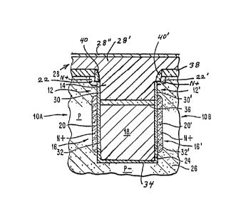
In accordance with the teachings of this ~-
invention, a novel vertical structure of the memory
circuit of FIG. 1 is illustrated in FIGS. 2 and 3,
wherein FIr~ 3 is a plan view of the structure and
20 FIG. 2 iS a sectional view taken through line 2-2 of
F~G. 3. AS shown in FIGS. 2 and 3, two dynamic
memory cells lOA and lOB are disposed on opposite
sidewalls within a trench 24 formed in a semiconduc-
tor substrate 26, preferably made of silicon and
having a P- conductivity. Cell lOA includes the
field effect transistor 12, the storage capacitor 16
and the bit/sense line 22, formed as an elongated N+
diffusion region within the semiconductor substrate
26 along the upper portion of a first sidewall of
30 the trench 24. A word line 28, preferably made of ;
doped polysilicon, tungsten silicide (WSi2)! or
titanium silic:ide (TiSi2), or a combination of a
doped polysilicon layer 28' and a silicide Layer
28", as indicated in FIG. 2 of the drawings, or o~
copper-doped a:Luminum, is disposed at the upper or
major surface of the semiconductor substrate 26
arranged orthol~onally with respect to the
i32~834
-8-
longitudinal axis of the trench 4 in contact with
the gate 14 of the transistor 1
The transistor 12 and the capacitor 16 are
located within the trench 24 on t:he first sidewall,
with the transistor 12 being disposed batween the
bit/sense line 22 and the storage capacitor 16. The
transistor 1~ includes the gate 14, which is also :
preferably made of P-doped polysilicon, tungsten
silicide (WSi2) or titanium silicide (TiSi2), or of
; l~ copper-doped aluminum, separated from the first
sidewall of the trench 24 by a thin insulating layer
30, pre~erably a triple insulating layer made of
silicon dioxide, silicon nitride and silicon
: dioxide, or a dual layer made of silicon dioxide and
silicon nitride. If desired, the gate 14 and the
word line 28 may form an integral unit, as indicated
in FIG. 2 of the drawings, and made in a single
process step. The storage capacitor 16 includes the
storage node 20 made in the form of an N~ diffusion ~:
region disposed alony the first sidewall of the
trench 24 and the conductive plate 18, which may be ~.
made of P-doped polysilicon including boron,
separated from the storage node or N+ diffusion
region 20 by a thin insulating layer 32, preferably
also a dual or triple insulating layer made of
; silicon dioxide and silicon nitride. The storage
: node or N+ diffusion region 20 acts as the source
~:~ and the bit/sense line or N+ diffusion region 22
acts as the drain of the transistor 12.
.
}o A layer of insulation 34 is disposed~between :
the bottom of the trench 24 and the conductive plate :
~ 18 to isolate the conductive plate 18 from the
:~ semiconductor substrate 26 and a layer of insulation
36 is preferably grown, to a thickness of about 1000
angstroms, as silicon dioxide on the top of the
polysilcon plate 18 so as to isolate the transistor
.
1321~3~
g
gate 14 from the polysilicon plate 18, and an
insulating layer 38, preferably made of silicon
dioxide, is disposed between the upper or major
; surface of the semiconductor substrate 26 and the
word line 2~, with silicon dioxide spacers 40 and
40~ insulating the gate 14 from the bit/sense lines
22 and 22', respectively.
The second dynamic memory cell lOB, also
located within the trench 24, has a ~ield effect
transistor 12' and a storage capacitor 16' disposed
on the second or opposite sidewall of the trench 24,
with the gate 14, the conductive plate 18 and the
word line 28 being common to both cells lOA and lOB.
The second transistor 12' includes the gate 14
separated from the second sidewall of the trench 24
by a thin insulating layer 30'. The storage capaci-
tor 16' includes the storage node 20', made in the
form of an N+ diffusion region and disposed along
the second sidewall of the trench 24 within the
semiconductor substrate 26, and the conductive plate
18 separated from the N~ diffusion region 20' by a
- thin insulating layer 32'. A bit/sense line 22',
formed as an elongated N~ diffusion region within
` the semiconductor substrate 26 along the upper
portion of the second sidewall of the trench 24,
~ serves as the drain of the field effect transistor
: 12', while the storage node 20 serves as the source
of the transistor 12'.
:,.
~ As more clearly indicated in FIG. 3 of the
-~ 3Q drawings, the bit/sense lines 22 and 22' extend in a
: vertical direction along the longitudinal axis of
the trench 24 and orthogonal to the dlrection of the ::~
word line 28.
It can be. seen from FIGS. 2 and 3 that two very
compact one device dynamic memory cells lOA and lOB
are provided on opposite sidewalls of the trench 24
132~ ~34
--10--
isoIated from each other, and from any adiacent
cells, wherein all elements of the two cells lOA and
lOB are located within the trench 24 except for the
connecting word line 28. The trench 24 may be made
as deep and as wide as nècessary to provide a
storage capacitor of desired size and a transistor
of desired switching characteristics. In one
arrange~ent of the structure of the present
invention, the depth of the trench 24 is preferably
7 microns, with a width of one micron, and the width
of the channel of the transistors 12 and 12' being -~
- one micron, with the length of the channel also
being equal to one micron. Each of the thin layers
of insulation 30 and 30' forming the gate insulating
lS medium of the transistors 12 and 12', respectively,
has a total thickness of about 18 nanometers, with
the thickness of the silicon dioxide layers each
being 5 nanometers and the thickness of the silicon
nitride layer being 8 nanometers when the insulating
layer 30 is made in the form of the triple
insulating layers. The thickness of each of the
insulating or dielectric layers 32 and 32' of the
storage capacitors 16 and 16'and of insulation layer
34 at the bottom of the trench 24 is preferably 13
nanometers, e. g., 4 nanometers of silicon dioxide,
7 nanometers of silicon nitride and 2 nanometers of
silicon dioxide. The layers of insulation 30 and
30', 32 and 32' and 34 may also be made of the same
materials and have the same thicknesses, if desired.
The N+ diffusion regions 20 and 20' each extend into
the substrate 26 about 150 nanometers from their
respective sidewalls of the trench 24. With a
spacing between adjacent cells of an array of cells
along the word line direction equal to one micron or
less and alon~ the bit/sense line direction, which
is orthogonal to that of the word line direction,
equal to one micron or less, the size of one cell at
the surface of the semiconductor substrate may be
1321834
made equal to two square microns or less, which is
produced when the lithographic line width is equal
to one micron or less. Furthermore, the capacitance
of each of the storage capacitors 16 and 16~ versus
the capacitance of the bit/sense line 22, assuming
64 cells per hit/sense line, prc~vides a very
desirable transfer ratio of abollt 10 to 20%.
FIG. 4 is a plan view of a~l array of cells,
each cell being of the type illllstrated in FIGS. 2
and 3 of the drawings, wherein like reference
characters refer to similar elements, with two cells
lOA and lOB aligned in the horizontal direction
along the first word line 28 and two cells lOC and
lOD aligned in the horizontal direction along a
second word line 28A. The space between the word
lines of the array, such as between the word llnes
28 and 28A is filled with any suitable insulating
`material 42, e.g., a polyimide or reflowa~le
borophosphosilicate glass (BPSG). The cells lOA and .
2~ lOC are also aligned in the vertical direction along
bit~sense line 22 and the cells lOB and lOD are
aligned in the vertical direction along bit/sense
line 22'. As is known, each of the word lines 28
` and 28A is connected to word decoder and driver
circuits 44 for selective actuation and each of the
bit/sense lines 22 and 22' may be connected to known
bit line decoder, precharge and sense amplifier
- circuits 46.
FIG. 5 is a sectional view of FIG. 4 taXen
30 through line 5-5 thereof and FIG. 6 is a sectional `~
view of FIG. 4 taken through line 6-6 thereof to
more clearly show the details of the elements of the
cells lOA, lOB, lOC and lOD of the array.
By referring to FIGS. 4 and 5, wherein FIG. 5
is a sectiona]. view taken orthogonally through the
.. . .. . ~
~32183~
-12~
trench 24 in an isolation region between storage
nodes of the cells, it can be readily seen that the
bit/sense lines 22 and 22' pass through the
isolation region along the upper portion of the
sidewalls of the trench 24 separated by the
insulating material 42 and that the N+ storage nodes
20 and 20' do not exist in the isolation region.
: The conductive pla~e 18 is disposed in the isolation
region at the botto~ of the trench 24 insulated from
the semiconductor substrate 26 hy insulating layers
32, 32' and 34.
By referring to FIGS. 4 and 6 of the drawings,
wherein FIG. 6 is a sectional view taken parallel to
a sidewall of the trench 24 through the storage
nodes 20' and the bit/sense line 22', it can be seen
that the bit~`sense line 22' indicated as an
elongated N+ diffusion region passes along the upper
.portion of the semiconductor substrate 26 over the
storage node 20' of both transistors lOB and lOD but
spaced therefrom, with the word lines 28 and 28A
aligned over the storage node 20' of the memory
. cells lOB and lOD, respectively. The word lines 28
and 28A are separated from the upper or major
surface of the semiconductor substrate 26 by the
insulating layer 38. ~The sectional views of the
polysilicon layer 28' and of the silicide layer 28"
of the word lines 28 and 28A may also be readily
seen in FIG. 6 of the drawings. The length of the
channel of transistor 12' of each of the memory
30 cells lOB and lOD can be seen as the distance .
between the N+ diffusion region of the bit/sense
: line 22' and the N+ diffusion region or storage node
20'.
,
As is known, to write into or read from a-
random access memory array as shown in FlG. 4, word
line decoder.and driver circuits 42 and bit line
1321834
-13-
decoder, precharge and sense amplifier circuits 44
of any known type may be used to select any one or
more of the cells lOA, 10B, lOC and lOD. Further-
more, it should be undarstood that the trench 24 may
contain hundreds of memory cells along each of the
two sidewalls thereof to which the bit/sense lines
~2-and 22' may be connected and that hundreds of
similar spaced apart trenches m~y be arranged
parallel to the trench 24 containing similar memory
cells to which the word lines 2~ and 28A may be
connected. The trenches 24 may be spaced apart by
one lithographic line, i. e., by as short a distance
as one micron or less. Furthermore, it should be
understood that in order to more effectively utili~e
the area of the upper or major surface of the
semiconductor substrate 26, bit line decoder,
precharge and sense am~lifier circuits 46 may be
located at one end of alternate trenches 24, while
the remaining trenches 24 have the bit line decodsr,
2~ precharge and sense amplifier circuits 44 disposed
at the opposite end of the trenches 24. If desired,
the word line decoder and driver circuits 44 may
also be located at different ends of the word lines
28 and 28A in a similar manner.
. - -:
Any known process may be used to make the -~
memory cells of the present invention. In one
particular process, boron ions with an energy of
10 Mev are implanted through the major surface of
the semiconductor substrate 26 to produce a
concentration of lE17 to a depth of about 7
micrometers. ~referably, an epitaxial silicon
layer of this thickness and doping is grown using
conventional tèchniques. Then a shallow trench
having a depth equal to about the desired width of
one of the bit/sense lines 22 and ?2' is etched into
the semiconductor substrate 26 by known reactive ion
etching techniques in a chlorine-based ambient using
an oxide masking layer 38 of about 4,000 angstroms.
By using known chemical vapor deposition techniques,
~.
- . :, ,
132183~
-14-
a relatively thick oxide layer, preferably silicon
dioxide, doped with about 1~ arsenic and about 1500
angstroms thick, is deposited conformally along the
sidewalls and bottom of the shallow trench. A known y
5 reactive ion etching process is then used to form
arsenic-doped oxide sidewall spacers 40 and 40', as
indicated in FI~S. 2 and 5 of the drawings. Again
by using reactive ion etching techniques, the
shallow trench is further etched to its full depth
lO as trench 24 illustrated in FIGS. 2 and 5 of the
drawings. A thin arsenic-doped oxide layer (also
about 1~ arsenic doped), about 150 angstroms thic~,
is deposited conformally in the trench 24, followed
by a reactive ion etch to remove the thin
15 àrsenic-doped layer from the upper planar surface of
the substrate 26 and from the bottom of the trench
24. The trench 24 is filled with any suitable
photoresist, and with the use of any Xnown
multilayer or multilevel photoresist (MLR) process,
20 including a non-erodable layer, a deep photoresist
; pattern of lines is cut, by any suitable etching
process, orthogonal to the longitudinal axis of the
trench 24 to a depth extending to the bottom of the
trench 24. This deep photoresist pattern of linès -~
is used to define the storage nodes 20 and 20', and
by subse~uently etching away the exposed thin
arsenic-doped oxide layer, e.g., with the use of
dilute buffered hydrogen fluoride, from the
sidewalls of the trench 24 within the deeply etched
30 photoresist pattern of lines, discrete segments of ~-
arsenic-doped oxide remain on the sidewalls of the
trench 24 for use in forming the storage nodes 20
and 20'.The remainder of the photoresist in which
the deep photoresist pattern was formed is now
removed and the trench 24 is refilled with a new
photoresist arld reactively ion etched uniformly down
into the trench 24 to a depth desired for the upper ~;
edge of the st:orage nodes 20 and 20'. With the
upper edge of the storage nodes 20 and 20' defined
by the level of this new photoresist, all thin
1321~34
--15-- r
arsenic-doped oxide layer is then removed from the
upper portions of the sidewalls of the trench 24
with the use of any appropriate wet etchant. Since
the arsenic-doped oxide sidewall spacers 40 and 40'
are much thicker than the thin arsenic-doped oxide
layer, spacers 40 and 40' will remain substantially
undisturbed when etching the thin arsenic-doped
oxide layer. The new photoresist is then stripped
or removed from the trench 24 and by using any
suitable drive-in process the arsenic from the thin
arsenic-doped oxide layer and from the thick
sidewall spacers 40 and 40' is introduced into the
semiconductor substrate 26 to form the storage nodes
2~ and 20' and the bit/sense lines 22 and 22',
respectively. Thereafter, the thin doped oxide
layer is stripped from the sidewalls of the trench
24 and the thin insulating layers 32, 32'and 34 are
deposited conformally within the trench 24 by
sequentially applying very thin layers of silicon
dioxide, silicon nitride and silicon dioxide, with
the layers 32 and 32' acting as the dielectric for
the storage capacitors 16 and 16'.
The trench 24 is then filled with doped
polysilicon and planarized by chemical-mechanical
polishing, and the polysilicon is etched to a
suitable depth within the trench 24 so as to
establish the upper surface of the conductive plate
18 at a level slightly below the upper edge of the
storage nodes 20 and 20', as indicated in FIG. 2 of
the drawings. In order to provide an electrical
contact area to the conductive plate 18, a portion
of the trench 24 is masked prior to performing the
last etching step. The upper surface of the
- conductive plate 18 is then covered with the layer
of insulation 36 which may be appropriately grown on
the polysilicon conductive plate 18 by any known
oxidation process, increasing the thickness of the
insulating layer 38 on the surface of the substrate
26.
~321~3~
-16-
,
The portions of the thin insulating layers 32
and 32' extending above the layer of insulation 36
are now removed ~y usiny any suitable wet etching
process and new thin insulating layers 30 and 30'
are deposited which will act as the gate dielectric
of the transistors 12 and l~'. However, if desired,
the extended thin insulating layers 32 and 32' may-
be used as the gate dielectric of the transistors 12
and 12'. The gate 14 of the transistors 12 and 12'
and the word lines 28 and 28' are now made by again
depositing doped polysilicon into the trench 24 and
onto the upper or major surface of the semiconductor
substrate 26, and then printing and etching the
polysilicon into parallel strips arranged orthogonal
to the longitudinal axis of ~he trench 24, as
indicated more clearly in FIG. 2 of the drawing. If
preferred, as stated hereinabove, the word lines 28
and 28A may include dual or multiple layers of
conductive material so as to provide more highly
conductive word lines 28 and 28A. In this instance,
after the polysilicon has been deposited as
polysilicon layer 28', about 4,000 angstroms thick,
for the word lines 28 and 28A and prior to etching,
a layer of tungsten silicide or titanium silicide,
about 1,000 angstroms thick, is deposited over the
polysilicon layer 28' to form a more conductive
layer 28" in the word lines 28 and 28A, as indicated
in FIGS. 2 and 6 of the drawings. A polyimide or a
reflowable insulating material-such as
borophosphosilicate glass is then used to fill the
voids in the trench 24 between the word lines 28 and
28A and planarized. This latter insulating material
may also be used to cover the word lines 28 and 28A
with a layer about 5,000 angstroms thick. As is
necessary, a f:irst level metal layer, a passivating
layer and a second level metal layer may be formed
on the top of l:he resulting structure in the usual
manner to provide appropriate electrical connections
to the various elements of the memory.
1321~3~
-17-
It should be noted that an appropriate mask is
needed after the arsenic-doped sidewall oxide
spacers 40 and 40' have been formed in order to
remove the doped sidewall spacer.s at the ends of the
trench 24 to separate the bit/sense lines 2~ and 22'
from each other. Furthermore, another mask is
needed after the arsenic-doped sidewall oxide
spacers 40 and ~0' have been formed to define an
expanded ion implanted region electrically connected
to the bit/sense lines 22 and 22' to serve as a
contact area for the bit/sense lines 22 and 22' at
the ends thereof. It can be readily seen in
accordance with the teachings of this invention that
an improved memory cell has been provided in a
vertical structure within a semiconductor substrate
requiring a very small cell substrate surface area,
i.e~, only two lithography squares by forming within
a trench or groove the storage means, the switching
means and the bit/sense line of the cell, with the
word line disposed on the surface of the
semiconductor substrate and arranged orthogonal with
respect to`the the longitudinal axis of the trench
or bit/sense line. With the word line disposed on
the surface of the semiconductor substrate, its
25 dimensions are not subjected to the restraints ~;
placed on it as it would have were it located within
a small trench, such as trench 24, and, therefore,
the word line can be more readily made as a thic~,
highly conductive line. This arrangement is
particularly important in memories since the word
lines in a memory array are very long and usually
significantly longer than the length of the
bit/sense lines. Accordingly, it is important for
high speed memories to have word lines with a
resistance which is as low as possible.
Another advantage of the very dense memory of
the present invention is that capacitive coupling is
minimized between the bit/sense lines because the
~321834
-18-
doped semiconductor substrate 26 and the word line
arrangements maintain a significant shielding
effect, not provided by other dense layouts, such as
that shown in the hereinabove cited commonly
assigned U.S. Patent 4,769,786, resulting in an
improved signal to noise ratio.
It can be further seen in accordance with the
teachings of this invention that a high density, two
; square mamory cell has been provided in a memory
array having a highly conductive word line which
uses simple, knbwn process steps. For example, the
process used does not re~uire forming thick oxide
layers deep within the small trenches, since as
described hereinabove, only thin insulating layers
need be formed in the lower portions of the
trenches.
.-:
While the invention has been particularly shown
and described with reference to preferred embodi-
ments thereof, it will be understood by those
skilled in~the art that various changes in form and
details may be made therein without departing from
the spirit and scope of the invention.