Note: Descriptions are shown in the official language in which they were submitted.
1322~41
-- 1 --
The present invention relates to a system and
method for improving the RFI noise immunity of electronic
circuits and, more particularly, to a system and method
for shielding the engine electronics used on internal
combustion engines from spark lgnition RFI, particularly
where the electronics are of necessity located in close
proximity to the RFI source.
It is well known that high voltage ignition
systems are one of the worst sources of radio frequency
interference (RFI). In many internal combustion engines,
electronic control modules are utilized to control such
functions as spark ignition and fuel injection. When
utilized in compact design environments, such as for
example in outboard boat motors, the electronic control
modules are often crowded under an enclosing cowling and
located unavoidably close to a very powerful source of RFI.
For example, the secondary side of an ignition
coil can develop 15,000 volts immediately before spark
plug gap breakdown and discharge. In some cases, the
voltage may even reach levels as high as 30,000 volts.
The wave front which is generated by an almost
instantaneous voltage drop from 15,000 volts to
essentially zero volts results in the radiation of
electromagnetic interference signals over a wide band.
Typically, however, there is a concentration of energy at
frequencies in the range of approximately 150 magahertz.
These instantaneous bursts of high frequency RFI can
induce voltages in nearby conductors, including the wires
to and from a nearby electronic control module. Such
voltage transients may be induced in nearby wires as a
result of the high currents at
:
- ' - . .
.
1322~4~
high frequencies accom~anying the spark discharge or
the stray capacitance coupling to a high tension lead
could also cause a voltage change in a closely
positioned wire. Thus, a 15,000 volt transient on the
high tension leads of an ignition system might easily
induce a 1500 volt transient in a lead to or from an
engine electronic control module which includes the
usual PC board construction. In a typical lead wire
having a typiGal characteristic impedance of about 150
ohms, a 1500 volt voltage transient will be accompanied
by a 10 amp current transient and an injection of a
current of that magnitude into a circuit is likely to
causei a potential change at that point in the circuit
relat;ive to other parts of the circuit.
It is, of course, known to use suppressor
spark plugs to reduce RFI noise from spark ignition
systems. However, because suppressor plugs may
occasionally not function as intended, a single
unsuppressed firing could generate a very strong RFI
signal and cause a serious electronic circuit
malfunction or failure. Also, in high performance
outboard motors using fast rise time capacitive
discharge ignition systems, the typical automotive
resistor-type suppressor spark plugs cause a drop in
power output plus a noticeable reduction in the
smoothness of engine idle. For this reason suppressor
plugs are not universally used in outboard motors.
RFI transients are particularly troublesome
in digital electronic systems. A voltage transient as
low as 5 volts is normally sufficient to change a bit
in a digital system from digital zero to one or vice
versa. Furthermore, a dropped or added digital bit may
become temporarily locked in a digital circuit if it is
not immediately self-correcting~ Thus, an improper
logic state may remain locked in for a significant
~`
~3220~
period of time, resulting in a control malfunction.
Analog circuits are also susceptible to malfunctions as
a result of transient RF~ vol.ages, for example, timing
circuits may be caused to operate out of proper
sequence by a transient voltage. Ordinarily, however,
analog circuits tend to be immediately self-
correcting. Thus, the problems caused by RFI are
generally much more serious in a digital circuit.
Electronic modules are often shielded against
RFI by enclosing them in metal housings. Such metal
housings do tend to protect the printed circuit board
of the module inside the housing from externally
gener;ated electromagnetic fields. Nevertheless,
elect;ronic modules used on internal combustion engines
still tend to experience problems with spark plug
RFI. One of the primary sources of trouble is in the
wires entering the module through the housing which
pick up and conduct into the housing the strong
transient voltages induced from the firing of the spark
plugs.
It is known ~o use RFI suppressing by-pass
capacitors to prevent high frequency voltage transients
on the wires from reaching the inputs of amplifiers,
logic gates, etc. on the PC board inside the housing.
Typically, however, such by pass capacitors are
located to merely shunt the RFI voltage transients
directly to the ground network on the PC board. These
transient voltages are accompanied by strong transient
currents and shorting the transient voltage directly to
the circuit board ground, via a by-passing capacitor,
will result in an instantaneous injection of an
electric charge at that point. As a result, the
potential at the point of injection will also
instantaneously change relative to other parts of the
ground network. Should the potential difference be
1322~1
high enough, e.g. about 2.5 volts or more, a logic
signal from one digital device located at one point on
the ground network may be read as at an opposite s~ate
by another digital device located at another point-on
the ground network, which is at a different relative
potential.
Among the wires typically entering the
control module through the housing is~ a ground wire
from the engine block. Often, the ground wire extends
directly to a connection on the PC board ground
network. However, transient high frequency electrical
charges induced in the ground wire are then carried
directly to the PC board.
The metal housing itself may also experience
induced voltages, resulting in a potential difference
between opposite ends of the housing. If all four
corners of the PC board inside are grounded to the
housing, as is often done in conventional design, the
potential difference across the housing could also
introduce disturbances to the PC ground network.
Also, shielded cables are frequently used to
bring low level signals into an electronic module. If
the conductive shield on such a cable is allowed to
pass directly to the PC board ground network, there
will be another potential source of induced transient
voltages being transmitted directly to the PC board
ground network.
Thus, attempts to provide RFI suppression and
shielding for electronic circuit modules has often been
ineffective, particularly in high RFI environments
where design requirements dictate close proximity
between the ~FI source and the electronic circuitry,
either digital or analog. The generally-accepted
assumption that the ground network for a PC board is
always a true system ground, even under the varying
1322~41
influences of RFI transients, is believed to be tha major
source of the problem.
In accordance with the present invention, a system for
suppressing induced RFI in an orderly and logical manner is
presented. The invention is based on the premise that
conventional suppression techniques which do no more than
facilitate the sudden flow of transient electrical charges
into the PC board ground network are only maxginally
effective.
The system of the present invention may be applied to a
con~entional electronic module which includes the usual PC
board or boards, enclosed in a metal housing and to which
external conductors are connected which extend through a wall
of the housing and are connected to the PC board circuitry.
The system includes an external ground connection (for
example, from the engine block) connected to the metal
housing. Transient electrical charges entering the module on
the ground wire will thus first be substantially dispersed
into the housing. If the ground wire continues on to the PC
board, very little transient charge will actually go to the
PC board. Each of the other conductors entering the housing
is provided with an RFI voltage shunt connecting the
conductor directly to the housing closely adjacent to its
entry point. Any high frequency RFI transient voltages
appearing on these conductors are thus substantially shorted
to the housing, that is, to a ground that is essentially
isolated from the ground network of the PC board or boards
comprising the electronic control module. In addition, a
second (level) RFI voltage shunt i6 inserted between each
conductor and the PC board ground network at the
-- 5 --
1322041
-- 6 --
point closely adjacent the connection of the conductor to
the PC board active circuit area itself. Any remaining
transient currents, not removed by the first RFI shunts,
will be dissipated. Finally, a single ground connection
is made between the ground network of the PC board and the
housing. In this manner, any induced potential
differential from one point on the housing to another
would not introduce a corresponding disturbance in the PC
board ground network.
Each of the first and second RFI voltage shunts
preferably comprises a non-inductive by-passing
capacitor. Connection between each of the first
by-passing capacitors and the housing is preferably made
via a common low-inductance RFI-intercepting ground bus.
The RFI-intercepting ground bus may be constructed
independently and conductively attached directly to the
housing or may comprise a conductive trace on the circuit
board isolated from the ground network for the active
circuits and independently grounded to the housing.
Additional isolation of the PC board from high
frequency transient currents if desired may also be
provided by inserting a high frequency series impedance in
each conductor between the first and second RFI voltage
shunts, that is, between the first and second bypassing
capacitors.
Should any of the conductors entering the housing
for connection to the control module include a shielded
cable, the conductive outer shield of the cable may also
be grounded directly to the housing at the point of
entry. Alternately, the cable shield may be grounded to
the RFI-intercepting ground bus.
The method of the present invention for
suppressing engine spark ignition RFI includes certain
basic steps which appear to be essential for effective
~322~41
suppression in high RFI environments, such as are encountered
in an outboard motor. The steps comprising the basic method,
as well as the optional additional steps, may be selected
dlepending on the severitv of the RFI, based on such
c:onsiderations as the proximity of the electronic control
module and the lead wires associated therewith to the RFI
sources, the lengths of the lead wires and their location and
relation to one another, etc.
This invention will be further illustrated by way of the
accompanying drawings, in which:
Figure 1 is a generalized schematic of an, electronic
control module, showing in illustrative plan view a two-sided
PC board and incorporating the RFI suppression system of the
present invention.
Figure 2 is a plan view similar to Figure 1 showing the
major conductors and other key elements of the suppression
system with the top side shown in phantom to better
illustrate the complimentary bottom side ground and supply
traces.
Figure 3 shows a portion of an electronic control module
utilizing an RFI-intercepting ground bus separate from the PC
board.
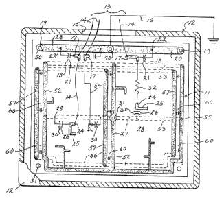
An electronic control module 10 includes a two-sided
printed circuit board 11 mounted inside a metal housing 12.
A group of conductors 13, comprising wires 14 or cables,
extend from the outside, through an opening 15 in a wall of
the housing 12 for eventual connection to the PC board 11.
One of the wires 14 typically comprises a ground connection
16 which, in the case of an engine control module, is
attached at its outside end to the engine block.
Each of the wires 14 entering the housing 12 through the
opening 15 is provided with a first termination 17 at a point
very closely adjacent its
-- 8
1322~41
entry into the housing. A first RFI voltage shunt 18
is connected between each first termination 17 and the
housing 12. The connection may be made directly to the
housing or may be intermediately attached-via a common
low-inductance RFI-intercepting ground bus 20 which is,
in turn, grounded directly to the housing.
Each of the first RFI voltage shunts
preferably comprises a first non-inductive by-passing
capacitor 21. Any high frequency RFI transient
voltages which may appear on the incoming wires 14 will
be substantially shorted out to ground via the housing
12 and ground connection 16 which are separated from
and n`ot likely to electrically affect the ground
network or the circuitry on the PC board 11. The
connecting leads of each capacitor 21 must be kept as
short as possible to provide low inductance and the
capacitor itsel must be of a non-inductive
construction. The intercepting ground bus 20, to which
the ground lead of each capacitor 21 is attached as at
22, may be a separate conductive strip or may comprise
a conductive ground trace 23 on the PC board 11. In
either case, the intercepting ground bus 20 or ground
trace 23 should be effectively isolated in a high-
frequency sense from the active circuits of the control
module 10. In addition, the ground bus 20 or ground
trace 23 should include multiple direct ground
connections 19 to the housing 12.
i From their first terminations 17, each of the
wires 14 typically continues to the PC board 11 to a
circuit connection 24 in an active circuit trace 25 on
the board. In lieu of wires 14 from the point of first
termination 17, the conductor may comprise a PC board
trace 54 forming part of an active circuit trace 25.
Very close to the connection 24 of the wire
14 tor trace 54) to the active circuit trace 25, a
.
;:
~322~
second shunt 26 is connected between the trace 25 and
the ground network 27 for the circuits on the PC board
11. The ground network 27, in the embodiment shown, is
shown as an isolated net~ork i-n Figure 2, and the -
second shunts 26 are attached thereto via ground
network connections 28 comprising conventional soldered
leads in plated-through holes extending through the PC
board. Each of the second shunts 26 also preferably
comprises a non~inductive by~passing capacitor 30.
Also, as in the case of the first capacitors 21, short
low-inductance leads should be used to connect the
capacitors 30 to the wires 14 (or traces 54) and to the
PC board ground network 27. The wires 14 or PC board
trace's 54 connecting the first RFI voltage shunts 18 to
the second RFI voltage shunts 26 inherently provide
some series inductance. This inherent inductance,
although small in value, is useful in forcing high-
frequency transient currents entering the module on the
wires 14 to flow through the bypass capacitors 21 to
the housing 12 via the RFI-intercepting ground bus 20,
rather than continuing on via the wires 14 or traces 54
into the active circuit area. To maximize the series
inductance in a simple manner, wires 14 of the smallest
practical diameter, or traces 54 of the narrowest
practical width, should be used. The first set of by-
passing capacitors 21 will thus have diverted most of
the high frequency transient RFI from the wires
directly to the housing (or to the housing via the
ground bus 20). Any remaining transient currents in
the wires 14 (or traces 54) will be relatively small
and will be diverted into the ground network 27 by the
capacitors 30. The ground network 27 should have low
resistance and low inductance to minimize local
disturbances of the potential of the ground network
when the remaining small transient currents are
~' .
. .
- . -- 10 --
1322~41
injected into it via the capacitors 30. Ideally, the
ground network traces should be substantially wider
than the active circuit traces and provide a gridwork
or pattern readily accessible to the ground network
connections 28.
Figure 2 shows the essentials of the
grounding system and the DC supply voltage network on
the bottom side of the PC board. RFI-intercepting
ground bus 20 is shown with three large-hole-diameter
feed-through pads S0. The large diameter holes in the
feed-through pads 50 are of sufficient size to allow PC
board `11 to be attached with mounting bolts to the
housing 12. The inside walls of the holes are plated
with copper or other suitable electrically conductive
material so that there is an effective electrical
connection from the RFI-intercepting ground bus 20 on
the top side of the board to an identical superimposed
RFI-intercepting ground bus 20 on the bottom side of
the board. Also, it should be understood that the
small feed-through type component mounting holes
typically provided for makin~ the ground attachments to
the capacitors 30 have not been shown in the ground
network 27. In addition, active circuit traces and
circuit components which could be included on the
bottom side of the board have been left out for
clarity.
Holes 51 are provided with PC board 11 merely
for mounting purposes.
The DC ground network 27 for the active
circuit area of PC board 11 is comprised of top side
trace 52 and bottom side traces 53. Top side trace 52
is itself comprised of three essentially vertical
traces and one horizontal trace, all joined into one
trace 52 as shown. The bottom side traces 53 are
electrically connected to top side trace 52 by means of
13220~1
feed-thru connections 55 and the large-hole-diameter
feed-through at 31, thus ~orming a DC ground network in
the form of a grid.
The DC supply voltage network 56 is comprised -
of top side traces 57 and bottom side traces 58, all of
which are electrically connected into a second grid
pattern by feed-through connections 59.
DC supply voltage noise-suppression
capacitors 60 effectively short the DC supply voltage
grid 56 to the DC ground network grid 27 for high
frequencies. Consequently, for purposes of
understanding the RFI-suppression features of the
invention, it is permissible to assume that the two
grids are merged into a single e~uivalent transient
voltage ground network 27 having a reduced level of
resistance and inductance for high frequency transient
currents.
The ground network 27 is connected to the
housing at only one point by means of a single mounting
bolt through the large-hole-diameter feed-through at
31. This precludes any transient potential difference
between one end of the housing and another from
inducing a potential disturbance in the PC ground
network 27, which might otherwise occur if there were
multiple ground connections between the ground network
and the housing.
It is, of course, understood that for
purposes of illustrative clarity no holes other than
the joining feed-through connections have been shown in
the overall grid structures of Figures 1 and 2.
Finally, the numerous DC supply voltage noise
suppresssion capacitors 60 normally used and as shown
in Figure 1, have not been shown on Figure 2.
Should any of the incoming wires 14 comprise
a coaxial or shielded cable, the conductive outer
- 12 -
1322041
shield should be grounded directly to the housing near
its point of entry. Such connection may be directly to
the housing 12 or to the ground bus 20 in the same
manner as with the ground connection 16. -
If the RFI transients to which the electroniccontrol module 10 is exposed are particularly strong, a
high frequency series impedance 32 may be inserted in
the wire 14 (or trace) between the capacitors 21 and
30. Such a series impedance will help to further
filter out relatively large high frequency transient
currents which might otherwise not have been adequately
shunted to the ground bus 20 by the first capacitors
21. ~n appropriate series impedance 32 may comprise a
ferrite bead or beads, an RF choke, a resistor, or some
combination thereof.
In Figure 3, there is shown~a portion of an
electronic control module which utilizes an RFI-
intercepting ground bus that is separate from the PC
board. In those applications where it may be
inconvenient or impossible to provide a conductive
ground trace 23 on the circuit board itself, the RFI-
intercepting ground bus may comprise a separate
conductive member attached directly to the housing 12.
In the embodiment shown, the intercepting
ground bus 20 comprises a separate terminal strip 33
attached to the inside wall of the housing adjacent the
opening 15 for the conductors 13. The opening 15 may
be surrounded with a conventional insulating grommet 34
through which the various conductors 13 pass. The
terminal strip 33 includes a conductive base 35
attached to the housing 12 with conductive fasteners 36
and spacers 37. An insulating strip 38 extends out
from the base 35 and includes a series of isolated
terminals 40.
. - 13 - 1322~
Each of the incoming wires 14 for which it is
desired to provide R~I sup?ression is severed
immediately after its entry into the housing and
attached to a terminal 40, as with a soldered
connection, to provide a first termination 17. The
soldered connection or the first termination 17 also
provides a point for connection of the other end of
lead wire 14 and one lead 41 of a first bypassing
capacitor 21. The other lead 42 of the capacitor 21
may be conveniently attached with a soldered or welded
connection 43 directly to the base 35 of the terminal
strip 33. The ground wire 16 may be soldered or welded
directly to the conductive base 35 of the insulating
strip at a convenient connecting point 44 or,
alternatively, could be attached to the base via one of
the fasteners 36.
RFI is not easily quantifiable nor are the
effects of RFI on digital or analog circuits easily
predicted. Nevertheless, the adverse effects of RFI on
electronic circuits, particularly digital circuits,
must be eliminated or reduced to levels which the
circuit can tolerate. The system and method disclosed
herein, though incapable of precise quantitative
definition, has been found in its minimum configura-tion
to provide fully adequate RFI suppression for
electronic circuits operating in extremely strong RFI
environments, namely, the compact environment of the
spark ignition system in an outboard motor.