Note: Descriptions are shown in the official language in which they were submitted.
i 3 2 ~
~, .
~.
INTEGRAL ACOVSTIC ~MISSION SE~SOR ~:~
FOR MANUFACTURI~G PROCESSES
~ND ~C~A~-CA~ oo~o~r~
BACRGROUND OF THE IMVE~TIOM
05 1. Field of the_InventionO
The presen~ inven~ion relates to
manufacturing machine or tool element~ and mechanical
components that have an:integrally mounted acoustic
emi~sions sensor to produce a ~iynal indicating
opexa ing conditions and para~eters.
2~ ~Descrlpt on _f he _ ior Art.
Manufacture of articl2s for consu~er and
- : industrial u~e may employ metal removal operations
~such as drilllng, milling, turning, and grinding),
metal forming and primary proce~ses (sheet rolling,
sheet forming, drawing,~and ironing, in addition to
forging and cold forming), as well a joining
processes (~uch as weldin~). In all of these
; operations, pla tic deformation i~ invariably
involved~ It occur in welding due to ~olidification
~ ~ shrinkage (small strain ~. In metal forming and
: other primary processes, larger shape changes occur
: which vary with the nature of the specific process
(small, medium, and large strains3. In metal removal
25: operations, plastic strains lmposed c n be quite
large. Grinding ~is an example. ~
Pla~tic deformation in all crystalline
materials involves defect processe traceable
ul~imately o the "line defects,'~ ., crystal
di~locatio~s. ~hape change or permanent ~train is
enforced by causing large scale dislocati n activity,
involving millions of dislocations per cm or
inch3
1322~11
- 2 -
In high strain-rat2 thigh speed) processes,
dislocation-lattice interactions involve phonons.
Substantial acoustic emis~ion can occur, a~, for
example, the loud noise accompanying metal fxacture.
05 At slower strain-rates, a rich variety o~ dislocation
interactions can occur, accompanied by ela6tic wave
emis~ion (acoustic emis~ion~. Many of these
phenomena are well discu~æed in recent publications
of worker~ at the National Bureau of 5tandard6.
Among the best known example~ o acoustic emi6sion
within the audible range is the "cry of tin" caused
by twining of individual crystals within a block of
tin.
Ceramic and ceramic-like materials (graphite
in a lead penril i8 an example) al80 produc~
substantial acoustic e~is ion as a consequence of
ela~tic energy release accompanying fracture. Large
æcale analog of this phenomenon are the s i~mic wave~
accompanying earthquakes. In thi~ cas~, the
displacements accompanying seismic wave propagation
are large enough to be detected by even crude
sei~mometersO
Similar surf2ce displacement~ acco~pany
acoustic emission in metals and ceramic object~. As
noted earlier, they are traceable to di~location-
dependent microscopic processes. The di~placements
produced are cmall.
Mechanical components ~ubjected to repeated
loading or cyclic stresses eventually fail by metal
fatigue. Substantial di~location activity i~ known
to accompany fatigue damage accumulation. When the
accumulating dama~e pxocesse~ can no lo~ger be
accommodated by internal microscopic changes and
atomistic displacement, failure initiation occurs~
`` ~322~
Subsurface and ur ace cracking in the ~icroscopic
scale, surface pittiny and other 6imilar damaging
event~ follow. Each of thsse failure~ inducing
events i~ accompanied by acoustic emi~ion.
05 Once a micro~copic or observable crack i~
formed, continued cyclic stres~ing or repeated
stressing induces bursts of acoustic e~ission
events. Discrete crack growth events and the
accompanying elastic energy release are responsible
for burst acoustic:energy emi~sion.
Acou~tic e~i~sion ~ensoræ hav~ been advanced
for mounting on machine tool and mechanical parts for
sen~ing acou~tic emissions. Conventionally, these
: sensors with inertial masses are mounted on a support
for the tool or ~achine ele~ent being monitoxed.
:: This results in mechanical;filtering of acouetic
emission signals between the mou~tlng interfaces of
~ the tool. Because ~he~acous~ic ~mis ion signals are
: relatively low lev 1, and in a relatively high
frequency range, the filtering results in the
:: inability to accurately f~llow the pattern Qf
acoustic emissîons from a given tool or machine
elementO Commercially available sensors are cvupled
to the o~jects, generally by pressing the sensor
against the urface of the object. Use of rubber
bands is common,:and someti~es adhesives are used to
hold the sensor in place. Of cour~e, any
imperfection in the interace between the sensor and
the object on which it is mounted al~o acts as a
filter, a~d thus various coupling agentæ, such as
liquids, are interpoæed between the ensor and the
object. Despite this, transduction efficiency i5
low, and at the present time the manufacturers of
exizting acou tic emission detection systems
~ 3 2 ~
recommend low noise, very high gain amplifier
systemQ. The problems associated with the high gain
amplifiers of course include any background noi~e,
and rather complex circuitry for obtaining any type
05 of a usable ~ignal.
The u~e of piezoelectric material for
sensing acoustic emi~sion6 is known, but these
ge~erally are mou~ted onto a sensor asse~bly having
an inertial mass. The sensor a~sembly is mounted
onto a support on the manufacturing tool or in the
location where acou~tic emi~sion sensing i8 de~ired.
A ~tudy of these types of devic~s is set forth in
Ferro Electrics, 1981, Volume 32, pag~s 79-83, in the
__
article entitled "Durable Lead A tachment Techniqueæ
for PVDF Polymer Transducers With Application to High
Voltage Pulaed Ultrasonics,'~ by Scott et al.
In particular, page 82 of the Scott article
shows a response of two different types of ~en~or~
including a commexcial broaa band acoustic emiscion
transducer, and th~ PVDF sensor under con ideration.
Thu6, i~ has been recognized that materials
have atomic and intermolecular structures that are
subject to shear, and void an~ discontinuity
producing events. Whe~ such events occur, they
release elastic strain energy in the form og stre-~s
waves. These waves propogate through the solid in
the forms of acouqtic waves, and velocity is
determined by the strurture and properties of the
solid. The acoustic waves may possess r~quencies up
to ~everal Mhz and are eventually dissipated by
tran3mission reflection and refraction at the
boundary ~urfaces of the solid and by irreversible
proces~es within the solid, such as molecular
shifts. Moni~oring of these sound wave or acous~ic
,:, , , ~ . . :,; .;: : ~ . :
::: . . i
: ; : , ; , ,: ., .: : :
1322~ ~
wave changes also yives information about friction
conditions between moving surface , and similar
acouRtic wave producing event~.
In the prior art, lead ~irconate titanate
OS (PZT) dete~tor with inertial mas~es ara used and
they provide for ~ubstantial "ringing" at the ends of
the signals being received as shown in the Scott
article cited above. Additionally, in that article
the PVDF (polyvinyldene flouride~ pie~oelectric :-
polymers were hown to produce a transducer without
s~-bstantial ringing:. :Both of these materials are
piezoelectric and they can be used for the present
integra~ed acoustic emission sensor that provides
real time analyzation of acoustic emissions o a
machining tool eLement.
SUMMARY OF THE I~VE~TIO~
The~present invention relates to an
integrated acoustic emission sensor for real time
monitoring of manufacturi~g~processes, utilizing a
:20 piezoelectric m ter~ial ens;or cQupled dire~tly to the
machining tooling element tha~ iæ desired to be
monitored. Use of an lnertlal mass, as in
conventional bulky acoustic emission ~ansors, is
completely dispen~ed with. The sensor is suitably
connected to sensing circuitry~for providing an
:: output signal as a fun~tion of:acoustic emis ions in
such tooling element.
Pre~erably, the sensor comprises a tool
ele~ent havlng a piezoelectric material deposited
thereon to form an integral sensor that will generate
electrical signals in response to stre -wav~ imposed
: diæplace~e~ts in the part itself. Quaxtz, PZT and
lithium compounds, as well as PVDF can be used for
sensor elements. The present sensors do not suf-f0r
~2~
from the limitations o~ mechanical intex~ace
filtering, or from the need to have complex mounting
techniques $or the sensors themselves. ~eed for an
addi ional inertial mass i~ al~o eliminated. By
05 eliminating the iner~ial ~assO the bulky conventional
A.E. Transducer is replaced with a compact planar
transducer, which is ea~ily mounted inte~rally in
tools and mechanical parts.
Aæ shown, the sensor i8 preferrably
deposited dir~ctly on the surface of the machine
element, such as a disposabl~ cutting tool insert, a
tool die or punch, a drawing die, or sîmilar tooling
or machine elements. The term "tooling element"
includa~ any type of machine work elemen~ that is
moved relative to a part bein~ workea upon7 which
move~ent r~sult3 in acou tic vibration~ that can be
sen~ed.
Variou~ applications of the integral sensors
are shown in the present pecification, and of course
any desired ~ype of ensing circuitry can be utilized
to provide the output signal that can be u~ed for
furth~r processing, control, alarms, or the like.
If tool fracture is being monitored, the
acoustic sensors of the present invention can also be
mounted onto thin mD~al substrates (without any
significant mas~ and lightly loaded again~t the tool
as is shown in one form of the invention, to provide
indications of ao~ual fracture. Present acoustic
emisqion gensors have significant mass whi~h limits
response. The mechanical fil~ering that occurs using
a thin metal strip pressed against the tooling
element is not a significant actor, primarily
because the sen~or is a very low mass sy tem.
Ihus, very a~curate acoustic emi~sion
. - . . .
~ 3 ~
sensors can be used in a wide variety of
applications. Daposited piezoelectric ~ensors can be
used for sensing the breakage of tools or in~erts,
the break or ~racture of the work ~at rial being
05 processed by the tool, aæ well as to detect
metal-to-metal conta~t in a lubricated tool system~
such as in a punch where the moving part~ generate
frictional force~ as a function of lubri~tion.
Sensors of this form cons~ructed directly on
mechanical components such as gears, c~m~, roller or
ball bearings, etc., allow pitting, wear, micro-
cracking and other deterioration proce~ses to alæo bedetected.
Thus, the acoustic emi~sion transducers can
be used to ~en~e fracture, cracking, micro-cracking,
pi~ting and friction involved in a process or an
operationl as much as changes in friction during
processing or mechanical component use.
The piezoelectric acoustic emission sensors
are ea~ily deposited in place in batch processes so
costs are kept low.
BRIEF DESCRIPTIO~ OF THE DRAWI~GS
Figure 1 is a per pective view of a machine
or cuttiny tool support having a disposable cutting
in~ert with sen30rs made according to the present
invention depoRited thereon;
Figure 2 is a perspective view of a typical
cutting tool insert or cutting tool showin~ integral
piezoelectric sensors made according ~he the present
invention mount~d on the top and side surfaces
thereo~;
Figure 3 is an enlarged:sectional view of a
tool insert as shown in Figure 2 showing in enlarged
scale the construction of the deposited piezoelectric
: : . - : .: .. ,: .: ~. : :
~ 3~2~
sensors formed thereon;
Figure 4 i9 a typical block diagram for a
circuit useful for-analyzing outputs fr~m sen~ors of
the present invention;
05 Figure 5 is a graphical representation of a
voltage signal that is delivered from a pieæoelectric
acou3tic emi~sion sensor made according to the
present invention at time of a change in conditions
at the cutting tool;
Figure 6 i a schematic represPnt~tion of an
unbonded, low ma~ ~50U~tiC emission seAsor ~trip
held in place on a cutting tool in~ert;
Figure 7 i6 a sectional view of the sensor
used in the device o~ Figure 6;
Figure 8 i a cross-~ectio~al repre3entation
of a wire drawing die with a acoue~ic emis~ion ~en or
made according to the pre~ent invention depo~ited
: thereon;
Figure 9 is ~ chematic cross-~ectional view
of a typical~deep:drawing pu~ch and die set, with
aroustic emission ~en~ors made according to the
pre~ent invention deposited on both the punch and the
die for sensing conditions that occur during the deep
draw for~ing operation;
Fi~ure lO i8 :a side view of a bearing having
a piezoelectric acou~tic emis~ion ~ensor made
according to the prese~t invention deposited thereon;
Figure ll is a sectional view taken on line - .
~ ll in Figure lO; and
Figure 1~ is a side view of a typical gear
co~ponent having an acoustic emi~sion:sensor made
according to the present invention deposited therein.
DETAILED DESCRIPTIo~ OF THE PREFERRED EMBODIME~TS
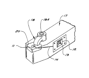
Figures 1-3 ~how a preferred embodiment of
13221~ ~
the present ~enRor on a cutting insert ~r cutting
tool 20 that is made in a conventional manner, and
generally rectilinear or circul~r disc in
configuration. U~ually auch cutting inserts axe made
05 of a suitable carbide, ceramic, or high ~peed steel
material. The cutting ins~rt 20 i5 held in a tool
holder 17 with a clamp finger 18, that is held in
place with a scxew 18A. The cutting insçrt 20 seats
down onto a ~houlder surface of the tool holder 17
and i8 clamped in place with the clamp lB. A corner
11 o~ the cutting insert 20 can be sharpened for
cutting, The cutting edge o~ the insert 20 can be
configured as desired.
The tool holder 17 has a receptacle 12 for
receiving and ~upporting a suitable int~grated
circuit chip 13~that ~an include signal conditioning
ana signal amplification in~tru~entation for the
sensors on the tool in~ert 20.~
: : An ~lectrical lead ~uch as that ~hown at 14
can be provided to the circuitry on chip 13. The
cutting in~ert 20 is shown in more detail in Figure~
2 and 3, and includes a first sensor portion 25
mounted on a surfac- 26 of the cutting insert 20, and
in addition it has ~ensors 28 and 29 shown on the
lateral side6 thereof. ~hese sensors can be on any
~ : desired ur~ace of the~cuttins insert, and a~ shown
: in Fi~ure 3 a sensor 30 i~ positioned on the Ride of
the cutting inæert oppo~ite from the sensvr 25. Each
of the senæors 25, 28, 29 and 30 shown are configured
in ~ubstantially the same manner. ~ach sensor
includes a deposited layer of piezoelectric material
that iB the active element. If a thin film
piezoelectric layer is to be used, the layer can be
deposited by radio frequency sputtering, reactive
:-. .. : ,, : :. , . . :. ..
~ 3 2 ~
-- 10 --
sputtering or other physical vapor deposition
techniques directly on the tool insert ~urfaces.
Suitable ma~king of course will be provided. The
pie~oelectric layer can be covered with a depo~ited
05 conductive layer, so that contact~ for taking off
signals can be ea~ily connected. Likewi~e, thick
film (silk-~creening) tech~ology can be utilized for
depositing the layer of piezoelectric material for
the sensor. A1BO bonding piezoceramic transducer
elements onto disposable cu~ting insert3 can be
achieved 60 long as the bond makes the 3ensor
integral therewith.
Each of ~he sen~ors is constructed
substantially identically and includes a depo~ited
layer of piezoelectric material indicated genexally
at 32, a conductive layer 33 that is deposited on top
o the piezoelectric layer ~or providing el0ctrical
interface, and an insulating protective layer 34
deposited over the conduc~ive layer 33. The cutting
insert 20 as shown, when it is working and cutting
material, will set up internal elastic wave emi6sions
fro~ a variety o dislocati~n in~eractions, and these
elastic wave emi sions are propagated as sound waves
throuyh the cutting insert to the exterior surfaces,
where they affect the piezoelectric layer 32 of each
of tha sensors at the interface 35 of the
piezoelect~ic layer and the cutting insert, the wave
compresses the piezoelectric layer and tha~ provides
the piezoelectric voltage effect which causes a
voltage di~ferential with re~pect to the interface
indicated at 36 between the conductive l2yer 33 and
the piezo~lec ric layer 32.
A~ previously explained, the piezoelectric
layer can be any desired type of piezoelectric
material, including YariOus polymers or oxide~
Additionally, the piezoelectric material in layer 32
can be deposited in an internal layer of the cutting
tool insert if the cutting in~ert i5 constructed in
05 layers. Zinc oxide i~ one example o~ a piezomaterial
fil~ ~uitable for construc~ing integral acou~tic
emi~sion transducer~ of the present invention.
Aluminum nitride, lithium niobate, PZT, or other
desired material~ also can be deposited or bonded to
the cutting in~ert~
The sensor layer thickness i8 substantially
enlarged in Figure 3, and actually i8 a very thin
film. The conductive layer 33 and the insulating
layer 34 are also quite thin, 80 that the cutting
tool insert i~ not substantia1ly enlarged.
If desired, a backing plate can be u~ed on
the underside of the cutting insert with an~opening
so that the sensor 30, or example, will fit in the
opening and i6 not ~ubjected ~o compressional forces
when the cutting i~sert is clamped into place.
The output from the piezoelectric sensor,
for example, the sensor 25, is connected through a
suitable lead 38 to ~ensing and processing
circuitry. For example, the circuitry can be that
~hown in ths block diagram of Figure 4. The sensor
is repres nted at ~5, and the signal coming along the
line 38 is amplified in the first staye amplifier 40,
and i8 ed to a fa3t Fourier transform analyzer or
other ~uitable analyzer circuitry indicated generally
at 410 The output of the analyzer circuitry is
proYided to a co~troller 45 that can be used for
monitoring a machine tool, for e~a~ple, ox
controlling other processes as desired. The
controller output alo~g the line 45 can be fed to an
. . :. ,: . ~ . Y
~ 3 ~
~- 12 -
actuator 16 or alarm, or a similar output module such
as a recorder ~or recording the acou~tic emissions
that are senæed. Thi8 circuitry i8 conventional, and
is shown by way of illustration only.
05 Additionally, Figure 5 i8 a graphical
representation of a typical output Erom an acou~tic
emission sensor mode accor~ing to the pres~nt
invention placed on a cutting tool in~ert such as
that shown at 20, and u ing a deposited zinc o~ide
film. The plot of Figure 5 shows time versua output
voltage/ and the spike shown at 48 is a typical
output that is sensed by the piezoelPctric transducer
during the fracture mode of the tool insert, bec~use
of acoustic emissions caused by such fractureO
These outputs from acoustic emission sensors
made according to the present invention have been
compared experimentally with outputs of standard
acoustic emission sensors. The time relation6hip of
the major ou~puts are identical betw2en com~ercial
acoustic emis~ion sensors and sensors of the pre~ent
invention which indicates that the acoustic emissions
~re being sensed by the integral sensors disclosed
herein. The present sensors provide a much yreater
output because of the lack of mechanical filtering
due to ~nterfaces and becau~e the ~ensors are
directly a-~ociated with the cutting insert or other
tooling element that i5 being monitored. In contrast
to the conventional acoustic emission (AE)
transducer, the present invention does not use an
iner~ial mass. By dispensing with the mass, a
sensitive transducer, compact in size and low in
cost, can be constructed on any manufacturing tooling
or mechanical component. Scope of AE monitoring for
::. :: .,, , , :.: .
1~22~1~
- 13 ~ :;
failure/~racture monitori~g and detection i~ greatly
expanded.
A modified form of the invention i8 shown in
Figure 6, wherein a tool holder 50 ha~ a standard
05 cutting in~ert or cutting ~ool 51 mounted thereon. A
clamp 52 is u~ed for clamping the cutting tool 51 in
place on its support surf~ce. As shown a hou~ing 53
i8 rece~sed into a provided re~eptacle below the
support ~urface 54 of the tool holder, and an
: 10 acou~tic emission sensor as~embly indicated generally
at 55 is supported with respect to ~he housing under
a biasing load from a light spring 56. The sen~or 55
comprises a layer o~ piezoelectric material deposited
onto a very thin metal ba~e that is substantially
masslesæ, so~that it does not respond to
accelerations, but ~enses acoustic emi~sion. me
contact of the piezoelectric material between the
surfa~e o~ the ~utting tool 51 and the ~urface of it~
moun~ing ~trlp is such that~the acoustic waves in the
cutting insert cause a voltage to be generated in the
sensor. ~he sellsor is madè the same as that shown in
Figure 3 except the layer of piezoelectric material
is depo~it~d on a ~trip of metal instead of the
cutting insert. The strip iB bia~ed against the
inser~ 51.
Figure 7 is a typical 6howing of the
piezoelectric: ~ensor 55, including 21 light metal
plate 58 that is substantially massle s, and a
suitable piezoelec~ric layer 59 deposited thereon. A
conductive layer 60 is applied as in Figure 3~ and if
de~ir d, an:insulative layer 61 may be deposited on
the sensor in the ~ame manner as in the first form of
the inventionO The light spring 56 i6 made so that
iS will 50ntact the conducting layer through an
. : .- ;- .. .,: - . :, ;..
.-: .. :: ,: ,- - : :
~32~
opening in the insulative layer 60.
An amplifier 63 can be mounted directly into
a tool holder in a provided receptacle, and as ~hown
a lead 64 coupled to spring 56 ca~ries the signals
05 generated by the acousti~ emi~sion~ acting on
pie~oelectric layer 59. m e sig~als at the amplifier
input are amplified and provided on an ampliier
output line 65 to suitable proces ing circui}ry~
This type of sensor 55 will work e~ficiently
only with a low ma~s ba~e or strip 58. ~arge mass
sensors cau~e exce~ ive filtering becau~e o
acceleration force6 on the sensor. The l~w mass,
deposited layer piezoelectric sen~or will provide
acou~tic emission sensing directly from a cutting
insert 51 or other ~achining element~
In Figure 8, a wire drawiny die 68 is shown
schematically, and is used for drawing a wire along a
central axi6 indica~ed at ~9. me die 68 has a die
opening 70 ~or ~waging the wire that is being drawn
to the right size. In this for~ of the invention,
the die 68 has an acoustic emi~ ion sen~or indi~ated
at 71 deposited directly on a surface 72 of the die
adjacent to the die opening. The sensor 71 is
constructed as shown in Figure 3, with a
piezoelectric layer deposited directly on the die.
The friction between the wire and the die
itself will cause vibrations and stre~s waves to be
set up, and these can be sensed as acousti waves by
the sensor 71 u~ing the inte9ral acoustic emission
sensing element or sensor deposited directly onto the
suxface of the die that is being used. A voltage "V"
will be generat d between leads ~hown in Figure 8.
In Figure 9, a ~chematic showing of ~ sheet
metal cup forming die 75 is shown. A punch 76 iB
~ . :: ~ .. . . `: . ` . , . :
~22~ ~
used ~or drawing a blank as it i8 moved through the
die. The die 75 has a die opening 78 through which
the punch 76 will be pushed for for~ing a blank
indicated generally at 80 into a deep d~awn cup or
05 the like.
As the punch 76 pushes the blank 80 through
the die openin~ 78, friction forces generate acou~tic
e~issions that are sensed with a ~uitable acoustic
~mission ~n80r ~2 compriBing a layer of
pie~oelectric material depo~ited directly on the die
75. A second acou~ic e~ission sensor 83 compri~e~ a
piezoelectric layer depoaited directly on the punch
76. r~he lubrication between the blank 80 and the
~urfaces of the die and punch can be determined by
sensing ~he changes in acous~ic emission6 as the
blank 80 i~q being formed. A hold down or pressure
~ad i~ æhown ~che~atically a~ 84 for restraining the
outer edge portions of the blank to control the
drawing operation. If ~he friction force increase
because of 2 lack of proper lubrication between the
blan~ and the surfaces supporting the blank, the
acou~tic emissions also increase in intensity a~d in
frequency~ The acoustic emissions will be accurately
sensed without mechanical filtering of the acoustic
~5 signals.
Figures 10 and 11 are views o~ a mechanical
component comprising a be~ring 90 that can ~e either
a ball or a roller bearing, with an integral acoustic
emission tran~ducer 91 placed thereon. The
transducer 91 may be deposited on the peripheral
surfaces (circumferential ~urface o~ the outer race,
or the lateral surfaces of either the inner or outer
race~ o the mechanical co~ponent to monitor
frictional conditions, lubrication, cracking and
.. ,.,:.: ~
~, ; , ,,
~~ 2 '~
micro-cracking on the ball or roller path. The
transducer al80 can detect pitting of the ball or
roller path pitting during operation of this and
similar mechanical elsments.
05 The acoustic emis~ion sensor or transducer
91 can be constructed as d~scribed before, by
directly depositing a layer of piezoelectri~ materlal
in place and using a conductive f ilm and in ulative
protective coating.
Figure 12 is a schematic drawing of a ge~r
component 93 with an integral acou~tic emission
tran~ducer 94 positioned thereon. As in the case of
bearings, acou~tic emission transducers are directly
depo~ited on an appropriate non-wearing surface of
the gear component. Continuous monitvri~g enables
identification of gear tooth wear, cracking, pitting,
and other deleterious events which ultimately lead ~o
component failure. The AE transducer can be applied
~o cam~ and oth~r machine elements as well.
- The integral sen~ors can be mounted directly
on tooling elements of various configurations,
including the use with cutting inserts or cutting
tools, punches, die6 and the like.
Other metal working tool~ also can have
integral sen~ors thereon. The integral acou~tic
emis~ion sensor6 or transducers may be used to ~ense
breakage of a tool, breakage or fracture of the work
material being proces~ed by a tool, as well as to
detect conditions of metal-to-metal contact in
lubricated tool ~ystems and tool and work piece
contact for cutting tool systems.
It should be noted that the sen~ors shown in
Figures 6 a~d 7, for example, having a separate base
on which the piezoelectric layer is depo~ited~ are
"~ "," : " "," ,~, ,, `:: ` ~ ,~ ", , " : :
~2~
primaxily used for high output signalB ~ 8uch as
occurs if a tool or metal part being worked would
fxacture~
me acoustic emis~ion signals obtained from
05 the sensors disclosed herein provide direct
informatiDn indicating conditions of a ~achine
tooling element. The ~ensors made accoxding to the
present invention give very high re~ponse t~ various
phenomena acting on tooling ele~ents. There is no
filtering by mechanical interfaces be ween the
tooling elements and their mounting , and thu~ direct
monitoring of condition~ can be obtained.
: Repetitive or cyclic loading i8 common in
mechanical component6. In ball or roller bearings, a
point on the raceway at the inner~or outer race
exp~riences high Hertz ~tresses as the ball or roller
traverse acro 8 tha~ point.
: In~gears, cams and other mach1ne elements,
~ similar cycIic loading is common. After everal
: ~ 20 thousand to several million loading cycles, fatigue
damage accumulation occurs and eventually leads to
sub-sur~ace or ~urface cracXiny, pitting, and other
de~ects. Formation of ~hese defects is invariably
accompanied~by acoustic emi~sion~
By~constructing the~ma sless, acoustic
emission tran~ducers disclosed here, continuous
monitoring and detection of failure proces~es is
ena~led.
In mechanical systems where failure has
; 30 catastrophic conse~uences (aixcraft engines, nuclear
reactor, etc.), continuous acoustic emission
monitoxing with conventional AE transducers is
common. By disclosing a method of con~tructing
integxal transducers and ~assless transducers, this
~322111
- 18 -
invention and the use of this invention a~ an
integral part of critical mechanical components
enhance the Rafety in advanced mechanical ~y~tem~. ;
Although the pr~ent invention has been
05 describ~d with reerence to preerred embodiments,
workers ~killed in the art will recogni~e that
changes ~ay be made in form and detail without
departing from the ~pirit and ecope of the invention.
~ - . . .. : . ; , ,
: .: . .. : : . -. : . ,, -
:: - - ~, . . . :
: ~ ~: : . .