Note: Descriptions are shown in the official language in which they were submitted.
` - 1 3 ~
,
TITLE OF THE INVENTION ~ .
F.lectricity-Light Transmitting Composite Wire
BACKGROUND OF THE INVENTION
Field of the Invention
This invention relates to an electricity-light
transmitting composite wire for transmitting both
electrical energy and optical signals.
Description o~ the Prior Art
Heretofore, in the~field of power transmission,
composite of optical fiber and electric wire have been
used. In a typical construction, an optical fiber unit
formed by gathering~a suitable number of optical fihers is
positioned at the center and a pluxality of metal strands
are twisted together around said optical fiber unit.
At present, such composites of optical fiber and
electric wire~are~limited in use to the field of power
transmissio~. It seems that the reason is that composite
wires having optical fibex and electric wire compounded
together are highly rigid and hence hard to handle and are
not so compact in form. Therefore, in the field of power
distribution including connection between two parts, they
cannot be used as such.
As is known in the art, optical fiber has the merit
of being capable of transmitting an extremely high density
optical signal despite the fact that it is compact in
.
. : :: : .... : ., ~ .. ; :: -:
~322~18
form. In contrast, in the case of electric wire, when it
is desired to transmit high electric energy or to transmit
electric signals or the like over a long distance without
sufering much attenuation, it is necessary to
correspondingly increase the cross-~ectional area of the
electric wire. Therefore, in a COmpQSite wire of optical
fiber and electric wire, if a compact form is to be
attained, this involves a reduction in the cross-sectional
area of the wire section, entalling a reduction in the
amount o~ electric energy which can be transmitted or
attenuation of electric signals to be transmitted.
SUMMARY OF THE IN~ENTION
Accordingly, this inven~ion is intended to provide an
electricity-light transmitting composite wire which is
capable of ~ransmitting optical signals and electric
energy in a high density manner.
An electricity-light transmitting composite wire
according to this invention includes a light transmitting
body mean~, such as an optical fiber, to tran~mit optical
signal~, and ~ ceramic type ~uperconductor which exhibits
superconductive phenomena at an operat.ing temperature and
which is compounded with ~aid li~ht transmitting body
means.
The compounding manners include one in which the
light ~ran~mitting body and the superconductor are
... -. ..... ,, . ,. ~, ,
. ~ . ,
13221~ g
compounded in a concentric construction and another in
which they are compounded in a planar laminated
construction.
In this invention, the transmission of optical
signals is undertaken by the light transmitting body,
while the transmission of electric eneryy or electric
signals is effected by the superconductor.
Thus, according to the invention, the transmission of
optical signals in a h1gh density manner is realized by
the light transmitting body, while in the superconductor,
electric resistance can be made zero, so that even if the
cross-sectional area is small, high electric energy or
accurate electric signals can be transmitted; such
electricity~light transm1tting composite~wire can be
constructed in compact fcrm.
Therefore, the field of application is widened to the
extent that it is applicable not only in the field of
power transmissicn but also in the field of power
distribution including connection between parts, and since
it is made compact in form, it is easier to handle.
- :
In a preferred embodiment, a stabilizing member is
inccrporated which ccntacts the superconductor to
stabilize the superconductive state.
As for the superconductor, it is preferable to use
one whose critical temperature is higher than 77 K
.
_ 3 _
~322118
(absolute temperature). Thereby, it becomes possible to
use liquefied nitrogen t77 K3, which is inexpensive, as a
refrigerant. Further, there would be a possibility of
using a superconductor which exhibits superconductive
phenomena at a temperature in the vicinity of normal
temperature. Thereby, the refrigerant can be dispensed :
with, and the composite wire can be prevented from
becoming increased in size owing to the refrigerant
passage or it becomes possible to use an inexpensive safe
refriyerant, such as water.
The superconductors which exhibit relatively high
critical temperature described above include a group which
is represented by the general formula AaBbCc ~where a, b
: and c are numbers indicating the proportions of
: 15 composition of A, B and C, respectively~, wherein A is at
least one member selected from the group consisting of the
group Ia, IIa and IIIa elements in the periodic table, B
is at least one member selected from the group consisting
o~ the group Ib, IIb and IIIb elements in the periodic
table, and C is at least one member selected from the
group consisting of oxygen, carbon, nitrogen, fluorine and
sulfux. In the above general formula AaBbCc, it is
preferable that the relation a x (average molecular weight
of A) + b x (average molecular weight of B3 = c x (average
molecular weight of C) hold. Presumably, a ceramic type
1~221~8
superconduc~or having a relatively high critical
temperature would have a layer-Iike perovskite t~pe
crystalline structure.
In addition, as for tha group Ia elements in the
5 periodic table, mention may be made of H, Li, Na, K, Rb,
Cs and Fr. As for the group IIa elements in the periodic
table, mention may be made of Be, Mg, Ca, Sr, Ba and Ra~
As for the group IIIa elements, mention ma~ be made of Sc,
Y, La, Ce, Pr, Nd, Pm, Sm, Eu, Gd, Tb, Dy, Ho, Er, Tm, Yb,
10 Lu, Ac, Th, Pa, U, Np, Pu, Am, Cm, Bk, Cf, Es, Fm, Md, No
and Lr.
As for the group Ib elements in the periodic table,
mention may be made of Cu, Ag and Au. As for the group
IIb elements in the periodic table, mention may be made of
15 Zn, Cd and Hg. As for group IIIb elements, mention may be
made of B, Al, Ga, In and T1.
As for the A in the above-mentioned general formula
AaBbCc, preferably it is at least two members selected
from the group consisting of the group Ia, IIa and IIIa
20 elemen~s in the periodic table. Further, preferably, the
B contains at least copper, and the C contains at least
oxygen.
These objects and other objects, features, aspects
and advantages of the present invention will become more
25 apparent from the following detailed description of the d
1 3 ~
present invention when taken in conjunction with the
accompanying drawings.
BRIEF DESCRIPTION OF THE DRAWINGS
Fig. 1 is an enlarged sectional view showing an
embodiment of the invention;
Fig. 2 is an enlaxged sectional view showing a
, .
stabilizing layer 3 and a pipe 5 added to ~he
electricity-light transmitting composite wire shown in
Fig. l;
Fig. 3 is a front view showing spiral groves 7 formed
in a superconductor layer 2;
Fig. 4 is an enlarged sectional view showing another
:
embodiment of the invention; and
Fig. 5 is~an enlarged sectional view showing a
; 15 further embodiment of~the~invention. ~
DESCRIPTION OF THE PREFERRED EMBODIMENTS
E~bodiments of the invention will now be described
with ~eference to the drawings.
First, an optical fiber 1 having a diameter of 0.5 mm
and formed of quartz or fluoride glass, as shown in an
enlarged seational view ln Fig. l, is prepared, and lt is
coated with~a 0.2 mm-thick superconductive layer 2. This
superconductive layer 2 is made form a ceramic type
supercsnductive~material having a composition such as, for
example, (La, Ba)2CuO4, (La, Sr)2CuO4 or YBa2Cu3O7_x.
: ~ :
'
~32211~ ~
Such superconductive layer 2 can be formed as by gas phase
process, such as sputtering or CVD, or by the so-called
sol-gel process involving condensation of alkoxide.
In addition, a protective layer (not shown) for the
optical fiber 1 may be formed between the optical fiber
and the super conductive layer 2.
The electricity-light transmitting composite wire 10
shown in Fig. 1, though thin as a whole, is capable of
transmitting optical siynals and electric energy in the
form of power or electric signals in a hi~h density manner
or in large amounts.
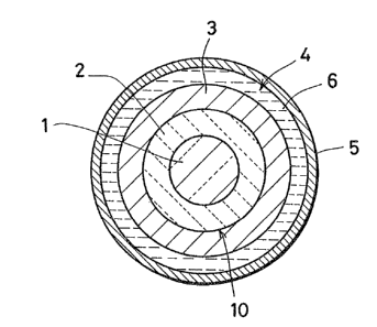
Fig. 2 is an enlarged sectional view showing other
,,
components added to the composite wire 10 shown in Fig. 1.
;~ ~ First, the superconductive layer 2 is coated with high
purity copper or aluminum, for example, so as to ~orm a
stabilizing layer 3 ~or stabilizing the superconductive
state of~the superconductor which forms the super
conductive layer 2. And the structure starting with the
optical fiber 1 and ending in the stabilizing layer 3 is
received 1n a pipe 5~with a sui~able clearance 4 defined
therebetween. The clearance 4 serves as a passage for a
refrigerant~6 used to cool the superconductor which forms
the superconductive layer 2 to its critical temperature to
put it in the su~erconductive state. The pipe 5 itself is
: ~
preferably formed of a heat insulating material or is
- 7 -
,. .. , , ,., .. i~
132211~
coated with a separate heat insulating material (not
shown). Further, the pipe 5 performs the function o
protecting the optical fiber 1 and the superconductive
layer 2.
In the description of the above embodiment, the
diameter o~ the optical fiber 1 is 0.5 mm and the
superconductive layer 2 is formed thereon; however, tb
provide magnetic stabilization o~ the superconductor
~orming the superconductive layer 2, it is preferable to
reduce the diameter of the optical fiber 1, for example,
to not more than 100 ~m.
As fox the means for magnetically stabili7.ing the
super onduct~ve state o~ the superconductive layer 2,
besides the measure of making the diameter of the optical
~iber 1 relatively small, a number of spirally extending
grooves 7, as shown in Fig 3, may be formed in the
superconductive layer 2 to divide the latter. The
dividing of the superconductive layer 2 shown in Fig. 3
may, of course, be ef~ected concurrently with reducing the
diameter of the optical fiber 1 to not more than 100 ~m as
described above.
Fig. 4 is an enlarged sectional view showing another
: embodiment of the invention. The compounding manner of
the composite wire 10 shown in Fig. 1 is such that the
light transmltting body (optical fiber 1) and the
. ~
. , ,
1322~.18
superconductor (superconductive layer 2) are compounded in
a concentric construction. In the embodiment shown in
Fig. 4, however, the light transmitting ~ody and the ;~
superconductor are compounded in a planar laminated
construction.
That is, the electricity-light transmitting composite ;
wire 20 s~own in Fig. 4 has a lisht transmitting tape 11
serving as a light transmitting body, and a
superconductive layer 12 laminated thereon. In addition,
the material of the light transmitting tape 11, and the
material of the superconductive layer 12 and the method of
producing the same can be made the same as in the
electricity-light transmitting composite wire 10 shown in
Fig. 1. ;
Fig. 5 is an;enlarged sectional view showing a
further embodiment of the invention.
In the~electricity-llght transmitting composite wire
30 shown therein, a reinforcing member 22 formed with a
plurality o~ grooves 21 is disposed at the center. The
xeinforcing member 22 is made, for example, of
fiber-reinforced plastic or metal. The grooves 21 are
foxmed so that they extend spirally on the outer
peripheral surface of the xeinforcing member 22. The
reinforcing me~ber 22 is received in a pipe-like sheathing
member 24 with a suitable clearance 23 defined
- , , . . ~. , ~ ,, ,. ., .. - .
, . , . - , : . . . .
.. , ~ ,
" ~22~18
therebetween. the clearance 23 serves as a passage for a
refrigerant 25 used to cool a superconductor (to be later
described) to its critical temperature to put it in the
superconductive state.
s In addition, if the rein~orcing member 22 is made of
metal, it itself can be used as a conductor. Further, if
a superconductor to be later described is disposed in
cont~ct with the reinforcing member 22 while forming the
latter of high purity copper or aluminum, then the
r~inforcing member 22 can be made to function as a
stabilizing member for stabilizing the superconductive
state of the superconductor.
In the composite wire 30 shown in Fig. 5, there are
two possibilities concerning wires denoted by the
reference numeral "26" and disposed in the grooves 21 of
the reinforcing membex 22.
The first possibility is that each wire 26 is in the
form of the electricity-light transmitting composite wire
10 shown in Fig. 1. The second possibility is that some
of the wires 26 are formed of optical ~iber while the
others are in the form of wires made of ceramic type
superconductor itself. In either case, electric enersy or
both electric and optical signals can be transmitted.
In the prev.ious description relating to Fi~ (La,
Ba)2CuO4, (La, Sr)2Cu04 and YBa2Cu307_x have been given as
-- 10 --
. . . ~ .:
., - .
i3~2118
examples of the composition o~ the superconductor. In
this connection, it has been found that a superconductive
material which belongs to the third example, or a
Y-Ba-Cu-O type superconductor and which has the ~ollowiny
composition exhibits a-higher critical temperature.
Respective powders of Y2O3, BaCO3 and cuO were mixed
together so that the ratio Y : Ba : Cu was 1 2 : 3, and
the mixture was then preliminarily sintered. Thereafter,
this prelimlnarily sintered body was crushed, molded at a ~
10 pressure of 100 bar and ~ired at 940C in the air for 24 ;
hours. The sintered body obtained by such firing
exhibited symp~toms of superconduction at 90 K. Thus, if ~ Y
this ceramic ty~e superconductive material is used as the
superconductive material contained in the superconductive
layer 2 or 1~ or the wires 26, extremely high operating
:: :
temperat~re is available.
In addition, in the composite wire 10 shown in Fig.
1, the superconductive layer 2 has been located outwardly
of the optical fiber 1. However, as another embodiment of
the invention, the posltional relation between the
superconductor and the light transmitting body may be
reversed.
Further, in~Figs. 1 ~nd 4, a single light
transmitting body and a single superconductor have been
~ 11 --
.. . : -
; . :: ~ - :
.. :, : .
- ~ ~ . : .
132211 8
formed; however, each component may have a laminated
construction comprising a plurality o~ layers.
Although the present invention has been described and
illustrated in detail, it is clearly understood that the
same is by way of illustration and example only and is not
to be taken by way of limitation, the scope of the present
invention belng limLted only by the terms of the appended
claims.
.
- 12 -
,- : : : : . :. :, ~.,. . : . .. :: .