Note: Descriptions are shown in the official language in which they were submitted.
~222~
The present invention relates to an apparatus for dete-
cting a read error of an optical recording medium which
includes a clock track, along with data track(s), having a
predetermined pattern of clock bits recorded thereon.
Aspects of the priorart and preferred embodiments o~ the
present invention will be described by reference to the
accompanying drawings, in which:
Figure l shows a block diagram of an arrangement of the
present invention;
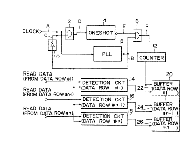
Figure 2 shows a block diagram of one embodiment of the
present invention;
Figurs 3 illustrates an enlarged ~iew of a portion of an
optical record.ing medium having data tra~ks and a clock track
disposed thereon, to which the present invention may be
applied;
Figure 4 is a timing diagram showing waveforms of the
main signals in the circuit of Figure 2; and
Figure 5 shows a block diagram of the arrangement of a
prior art PLL circuit.
An optical recording medium has been attracting a good
deal of public attention, which has a data recording surface
- 1 -
~ 32~2~
having optical alteration pattern~, such as light and dark
pits formed thereon to represent digital dataO The optical
recording medium realizes a large capacity of memory because
of its high density data recording capability. This led us
S to a consideration of not only a disc type memory but also a
card type memory.
In the card type memory or optical memory card, recor-
ding is done by forming optical (or magnetooptical~ altera-
tions in response to data to be recorded at discrete spots onthe surface thereof, and then a light beam, s~ch as a laser
beam, is projected thereonto to read the alterations.
Specifically, fine unevenness or light and dark patterns
are provided on a surface of a recording medium or card onto
which a light beam is projected to recognize the recorded
data according to the difference of reflectivity, refractive
index, or transmissivity of the medium to the projected light
beam. Alternatively, the recording medium may be
photothermo-magnetically recorded and the recorded data may
be read depending upon the change of polarization of the
projected light due to the magnetooptical effect.
- - la - --
j~\
. ~ ,
132~2~L~
In ju,Ytapositi.on with each of the data tracks of such
an optical memory card there are provided a clock track for
synchronization ,in a data wri-te/read operation and a -trac-
king guide l.ine as a rererence for causing the o~t~cal beam
of' an op-t:i.cal readi.ng system -to rollow the track accurately.
The write/read t.Lm.ing Or -the opt~cal recording med:i.um
.i.s conventionally determined by a clock signal derived from
a detector dedicated for d~tec,ting clock bi.-ts Or the clock
track.
Incidentally, ir the clock is not accurately read in
reading the clock track Or the optical record~ng medium by
reason Or dust, scratch or the like on the optical recording
medium or fluc-tuat:i.ons Or the moving veloGity Or the recor-
ding medium relative to -the op-tical reading system, then i-t
will be difricult to accurately achieve the write/read ope-
ration. An absence Or the clock during a short term or
relatively slow rluctuations Or the velocity can be dealt
with by using a phase locked loop (PLL) circuit whi.ch pro-
duce,s a cloc3s of a frequerlcy synchronized with the input Or
the read out or raw clocls.
Figure 5 illus-trates a typical arrangement Or a prior
art PLL circuit. The PLL circuit 66 comprises a phase
comparator 52, a low pass filter (LPF) 5L~, an amplifier 56,
a voltage con-trolled oscillator (VCO) 58 and a l/N f'requency
divider 53. This circuit compares, in phase, a received
input signal with an output of the divider 53 so as to match
the phase through controlling the VCO 58, thus producing, at
the output thereof, a clock Or a frequency Or N times Or
that Or the input signal.
~ lowever, ror a long--term absence Or the raw clock or
or an abrupt change Or the relative rnoving velocity Or -the
med.ium the PLL circui-t could not ensure -the accurate data
~ reading and may fall into an out-of-loclsed sta-te.
`; 2
~ . ' ' '
,
~3~22l~
The present invention provides an apparatus for
detecting a read error of an optical recording medium which
detects disorder of a clock for a data reading operation so
as to acquire normal data only~
In accordance with the present invention, as shown in
Figure 1, there is provided an apparatus for detecting a read
error of an optical recording medium, provided with a reading
device which reads data recorded on a data track of an
optical recording medium 60 to thsreby store the read data in
memory means 68, the apparatus comprising:
a PLL circuit 66 responsive to a read clock from said
optical recording medium 60 for generating a clock synchro
nized with the read clock;
address updating means 64 for updating a write address
or said memory means to store said read data therein in
synchronization with the output clock from said PLL circuit
66;
out-of-locking detection means 62 for detecting the out-
of-locked state of said PLL circuit 66 in response to the
read clock and the output clock from said PLL circuit 66; and
address updating suppression means 63 responsive to a
detection signal from said out-of-locking detection means 62
for suppressing the address updating of said address updating
means 64.
The optical recording medium 60 may have a plurality of
data tracks disposed thereon in parallel to each other and a
plurality of memory means 68 may be provided, each o~ the
memory means corresponding to the respective one of the
plurality of data tracks and being commonly connected to the
address updating means 64.
Accordîng to the present invention, data being read out
- 3 -
~;~
~' ~b
~3222~6
of the op~ical recording medium is continued to be stored
into the memory means as lony as the locked state of the PLL
circuit is maintained. Once an out-of-lo~king state of the
PLL circuit is, however, detected it is assumed that the
clock for data reading has fallen into disorder, and then the
address updating for storing the read data is suppressed so a
: to acquire normal data only at any time.
Since restoration of normal clock input to the PLL
circuit will cause the PLL circuit to resume its locked state
again, it is not considered in the normal operation on the
optical recording medium that the PLL cirruit is kept in the
out~of-locked state unusually for a long time. Therefore, it
is preferable to provide means for automatically removing the
suppression of the address updating after a lapse of time
during which the PLL circuit is assumed to resume its lo¢ked
sta~e agai.n after losing it. This means will enable the
apparatus to continue to acquire the succeeding data. --
22~$
Now, one preferred ambodiment of the present invention
will be described in detail referring to the accompanying
drawings.
Although the optical recording medium is assumed to be
an optical memory card in this embodiment, it will be appre-
ciated that the present invention may be applicable to other
types of optical recording medium.
The optical memory card to which the present invention
is applied comprises, as shown in Figure 3, a clock track 30
having a sequence of clock bits 32 disposed at regular
intervals in a row and a data track section 40 provided in
parallel to the clock track and including a plurality of data
rows l-n. The clock track 30 is also used as a ~racking
guide line. Alternatively, the guide line in this embodiment
may be provided separately from the clock track.
Structure of the Embodiment
Referring next to Figure 2, there is shown a block
diagram of one embodiment of the present invention.
In this invention the out-of~locking detection means 62
in Figure 1 comprises an inverter 10, an AND circuit 2, and a
one-shot circuit (monostable-multivibratvr) 4. The oneshot
circuit 4 also operates as means for cancelling t~e assertion
o~ an address-updating suppression signal after a lapse of
predetermine time after the assertion. The address updating
means 64 and the address updating suppression means 63 in
Figure 1 comprise an AND circuit 6 and a counter 12,
respectively. Also, the memory means 68 and the PLL circuit
66 in Figure 1 comprise buffer memory 20 and a PLL circuit 8
(N=l), respectively.
The AND circuit 2 has one input for receiving a read
clock A derived from the clock track on the optical recor-
- 5 -
.~P 'i
,~
. . .
,~:
,:
~3~2~$
d:i.ng med:Lurn ~nd another i.nput for receiving -the inverted
output signal C via the inverter 10 frorn the PLL. circuit 8.
In response to an output D of -the AND circuit 6, -the one-
shot circuit ll generates a negative-going pulse E of a
prede-termined duration at the rising edge of -the output
pulse of -the si.gnal D. The AND circuit 6 generates an
output F as a count-up signal to the counter 12 in response
to bo-th an output E of the one-shot circuit 4 and an ou-tput
B of the PLL circuit 8. The counter 12 provides its outpu-t
data as an address for each burfer 22, 2LI, and 26 within the
bufrer memory 20. Data input to each Or -the bufrer 22, 24
and 26 are Or binarlzed versi.on of the signals read out Or
the data rows 1-n on the optical recording medium 60 through
data detection circuits 14, 16 and 18. l'he capacity Or the
buffer memory 20 may be determined depending on the applica-
tion.
Operation of the Embodiment
Referring now to Figure 2 and Figure 4, -the operation
Or the circuit shown in Figure 2 is described hereinafter. .:
Figure 4 shows a timing diagram Or the main signals o~ the
Fi.gure 2 circuit.
The period T1 indicates a normal operation period of
the PLL circuit 8 which is being kept i.n its locked state.
During this period, the read clock A and the output B of PLL
circuit 8 are Or the same frequency and matched in phase,
that is, the clock A and the inverted signal C are 180
degree shifted in phase from each oth.er. As a result, the
AND circuit 2 generates no pulse at its output, maintaining
the output E of one-shot Ll at a high state. The high level
outpu-t of the one-shot 4 causes the AND circui-t to pass
therethrough the ou-tput B Or -the PLL circuit 8 as a signal F
wh:Lch in -turn drives the counter 12 to count it up. Thus,
the address of the buf`fer 20 i5 updated to sequentLally
.:
:~3~22~
store :in the updated address the read data from the optical
recording medium.
Now assuming that it is impossible to read -the clock
b:its at the end Or the period T1 and the PLL circuit ~ has
fallerl in~o the out-o~-locked s-tate after the lapse of -the
period T2, then in -the following peri.od T3 -the signal A will
not match in phase with the si,gnal B, thereby producing
pulses 82 in the output D Or the AND circuit 2.
At the rising edge Or the first pulse Or the pulses 82,
the one-sho-t Ll iS driven to genera-te a negative going pulse
Or a prede-termined dura-tion in its outpu-t E (the trailing
edge thereor is not shown in Figure 4 ) . The low level Or
the signal E causes the AND circui-t 6 to prevent the output
B from passing therethrough, thus suppressing the address
updating on -the coun-ter 12. Simultaneously, data writing to
-the burfer 20 is also suppressed (not shown).
After the lapse Or the output period of the negative-
going pulse 80 on the output E, the signal E will go bac~ to
its high s-ta-te, allowi,ng the signal B to pass through the
AND circui-t 6. At this time, the PLL circui-t 8 is consi-
dered to have already been restored to its locked state.
Althou~h one preferred embodiment i.s described hereln-
before, i.t will be readily appreciated tha-t many changes and
modificatiolls can be made without departing from the scope
or spirit Or the invention. For example, while a plurali,ty
of the data tracks are read at the same time in the above-
described embodiment, only one data track may be read a-t any
time.