Note: Descriptions are shown in the official language in which they were submitted.
- 11 3~23~
DIGITAL KEY TELEPHONE SYSTEM
The invention is in the field of small talophone systems and
the like, especially those sometimes referred to as key telephona
systems. More particularly, aspects of the invention relate to
signalling and supervision messaging functions in a digital key
telephone system, one example of which is disclosed in a Canadian
patent application entitled "Digital Key Telephone System",
serial number 67a,764, which was filed on September 28, 1988 by
George Irwin et al. and another in a Canadian patent application
entitled "Digital Key Telephone System", serial number 581,393,
which was filed on October 26,1988 by David J. Robertson et al.
The invention also relates to relocation andJor replacement
of terminal apparatus in telecommunications systems including,
but not necessarily limited to, such key telephone systems, and
is especially concerned with reassignment of administrat-ive data,
~or example, features, when a station or terminal apparatus is
moved physically ~rom one port to another within the same
exchange or ksy system.
Some examples of small telephone systems have been generally
referred to as key telephone systems. Traditlonally a key
t01ephone system is provided by extensive telephone line and
control lead wiring between key telephone sets. Each key
telephone l-ine extends to a telephone exchange. Each of the
telephone sets includes a plurality of push button switches or
keys, each for connecting the telephone set to a particular
telephone line among a plurality of telephone lines routed to the
key telephone set. The switching function of line selection is
mechanically provided and distributed among the key telephone
t
.
: ` `
."~ ~ . : ':
~3223~
sets. Any features in addition to plain ordinary telephone
service (POTS) must be added on a per line basis. ~rhe primary
advantage o-f these systems is economy with small size. However,
if such a system is required to expand along with the
organi~ation it serves, over a time it eventually becomes more
expensive on a per line and feature basis than a private branch
exchange would be. Key ~elephone systems are also
characteristically of the analog signal -type, and therefore are
impractical to interface with an ISDN as will likely be desired
by business customers in -the near fu-ture.
So far as those aspects o-F the invention concerned with
replacement and/or relocation in telecommunications systems
generally are concerned, most telephone sets or other terminal
apparatus nowadays are connected into the sys-tem by jacks, so it
1~ is a simple matter for the user to unplug a terminal apparatus
and reconnect it at a ~ifFerent port. Of course, if those
attributes of the terminal apparatus not resident in the terminal
apparatus itself are to be retained, corresponding administra-tive
changes must be made at the switch or, in the case of a key
telephone system, at the key switch unit. Existing systems
require the intervention of a skilled craftsperson to e~fect such
changes, typically by locating the feature set of the terminal
apparatus at the vacated port and assigning it to the new port.
This involves high costs and may incur delays. A similar
situation arises if the user replaces the-terminal apparatus wi-th
a new set i.e. new to the system rather than being relocated from
another port. Usually this would be done to replace a defective
se-t. Providing that they are of the same type, the new set will
'' . . ~ ~,. ' '` .
', " ` ' "' ' `
' . ` ` ' ~ ' .' ' ` " ' ' " . ~ ~ '
~3~ 39 ~
need to inherit the old set's administration data and, where
applicable, intercom number.
One object of the invention is to provide a-telephone system
wherein the functional advantages of key telephone systems and
digital signal communications are co-existent via station or
terminal apparatus connected to the system.
Another object o-f the invention is to provide for relocation
and/or exchange of sets without necessarily involving
administrative assistance by a craftsperson.
In essenc0, an example of the key telephone system includes
a central unit (KSU), and a number of terminal apparatus or
stations. S-tations may be, but are not limited to be, telephone
sets. Other forms of stations include data sets and interface
units to C.O. trunks. A general purpose computer, For example
a personal computer, may act as a station, with a suitable
interface unit. Stations are connected to KSU ports using
digital signals over twisted wire pairs. Some stations may
physically be part of the KSU, and be connected thereto by means
other than twis-ted pair. The KSU itself may include more than
one physical unit.
A primary function oF the key telephone system is to provide
point to point communication between the stattons, in the form
of switched, bidirectional, 64 kb/s channels. In one example,
each station has access -to two such channels. Each station also
has access to a 16 kb/s S and S channel used for system purposes
such as signalling and supervision. Each station, and the KSUl
contain some form of processing device, for example, a software
controlled microprocessor, or a logic network. The S and S
- - ,. . ~ .
- . . .
~ 32~3~ ~
channel allows one station at a -time to send a digitally encoded
message to the KSU. More speci-Fically, it allows the processing
device at the station to send such a message to the processing
device in the KSU. This reference to processing devices should
be assumed wherever the action oF a station or the KSU is
mentioned. The S and S channel similarly allows the KSU to
send a message to any one or more s-tations.
Each message is of a defined Format. In this example there
are two Formats, each of which require control information.
Depending on the control information in an incoming message to
the KSU, the KSU may retransmit that message to stations as just
described. Hence, a station may indirectly send a message to any
other station or to all stations, by relying on this KSU
operation.
The KSU operates in accordance with information contained
in the messages, to set up and tear down 64 kb/s circuit
connections between stations. Stations use such a connection for
PCM voice, or For data, or as another means to exchange messages.
The operation of a station is controlled directly by the
processing element at that station. The processing element runs
a low level program, and oay run higher level programs. The low
level program controls indicators and other devices at the
station, senses the state of input devices, and handles
generation and interpretation oF messages. A higher level of
program may control the sequences of operation of the station,
and co-operate with other higher level programs at other stations
or in the KSU to provide desired operation o-F the key telephone
system as a whole. The behaviour oF a station is determined by
'' ' :. ' '~ ,~ ' '
,
~ 3~23~
.~
the program runnin~ in that station, or by messages received -from
a program running in the KSU. The operation may be wholly or
partially determined by a program running in some other station,
including the case where that station is attached to or
incorporates a general purpose digital computer.
Since the behaviour of a station may be determined by tha
program running in another station, it is possible to add new
types of stations, as such become available, or to install new
software in existing stations, to affect the behaviour of
previously connected stations. Thus an added station may provide
new features, possibly requiring novel sequences of keystrokes
and display and indicator operation. The new feature is or may
be made available at existing stations without reprogramming
those stations or the KSU.
The added station providing the new feature may in fact be
a reprogramrnable device such as a personal computer. Thus new
features may be added solely by software change or addition in
an attached computer system, by techniques generally available,
without participation of the key telephone system manufacturer
or vendor. Of course, all of this extreme freedom of access to
and control of the communication functions and features may be
subjected to the typical security and priority fetters.
The invention is embodied in a key telephone system, for
providing digital signal communication paths between a plurality
of ports and for providin~ a signalling and supervision link
between, any of said ports and a processing device in the key
telephone system. The key telephone system includes
communication paths being operable to provide n pairs of time
~223~
division multiplex transmit (TD~T~ and time division multiplex
receive (TD~R) channels, each channel including a plura'lity of
bit positions. At leas-t one TDMT, TDMR channel pair is
e~clusively associated with each port. Each said TDMT channel
and said TDMR channel includes a signalling and supervision (S
and S) bit position9 in said plurality of bit positions. A
swikching means is operable to provide communication paths
between ones of the TDMT and TDMR channe'ls, to the exclusion of
said S and S bit posi-tions, as directed by the processing device.
An interface means, responsive to the processing device,
transfers informa-tion from the S and S bit position of a selected
TDMT channel to the processing'device and transfers information
from the processing device to the S and S bit position of at
least one of the TDMR channels, independently of the
communication paths provided by switching means.
A key telephone system, in accordance with the invention,
comprises a plurality oP ports for connection of any o-f a station
apparatus and an interface apparatus, each apparatus including
a processing device for controlling its functions. A synchronous
communication medium provides at least one bidirectional
communication channel and a message channe'l at each port. A
synchronous switch means transfers inPormation between selected
ones of the bidirectional channels in response to control
signals.
A central processor routinely identifies message channels
from which a message from one of said processing devices is
receivable, and in response ~o a received message, at least
generates one of khe control signals and at least one address -Por
.
. ' ~
~ 2~
defining a message channel for which a message for a
corresponding one of said processing dev-ices is deskined. An
interface means identifies a request to send, in response to a
first predetermined signal characteristic in one of the message
channels, previously identified by the central processor, for
soliciting and receiving said message. The interface means also
transfers destined messages to message channels as directed by
the central processor.
The invention is also a method of operating a key telephone
system having a central processor and a plurality of station
apparatus, each of said station apparatus having a processing
device for controlling functions of the station apparatus in
response to key control action of a user origin and in response
to messages received via the central processor. The method
comprising the steps of:
a) providing at least one bidirectional time division
multiplex channel in association with each of the station
apparatus;
b) providing at least one time division multiplex message
channel in association with each of the station apparatus;
c) routinely selecting one of said station apparatus for
transmission of a message via its associated message channel;
d) exchanging call set up messages between the central
processor7 a calling station apparatus and a called station
apparatus; and
e) in response to a predetermined message, from the called
station apparatus synchronously exchanging information between
.. .. ..
'''," :, " ' ,'
''~' '"'' ' .'"" .
~3223~ ~
the bidirectional time division multiplex channels associa-ted
with the calling and called s-tation apparatus.
The invention is also a method of signalling and supervision
communication in a telephone syskem having a central proc~ssor
and a plurality of ports, each being available for connectiQn of
an apparatus thereto, each such apparatus including, a processing
device for controlling functions of the apparatus, and an
interface device for exchanging signals in an operating signal
format of the port. The method comprises the steps of:
a) providing at least one time multiplexed message channel
in association with each of the ports;
b) roukinely selecting one of said apparatus for
transmission of a signalling and or supervision message via its
port associated message channel; and
l~ c~ exchanying messages, in a predetermined one of a
plurality of message protocols, between the central processor and
said apparatus.
The invention is also a method of communicating
signallin0 and supervision messages in stimulus and functional
20, protocols in a telephone system having a central
processor and a plurality of ports, each of the ports being
available for connec-tion of an apparatus, each apparatus
including a processiny device for controlling -functions of the
apparatus in response to reception of signalling and supervision
messages in one of said stimulus and functional protocols, and
an interface device for exchanging signals in an operating signal
f~rmat of the port. The method comprises the steps of:
:~ .
'
,
~22~
a) prov-iding a-t least one time mul-tiplexed message channel
in associa-tion with each port;
b) routinely selecting one of said ports for transmission
of a message -from its associated apparatùs, and in the central
processor receiving a message, -from the selected apparatus, said
message being in one of said stimulus and functional protocols;
c) in the central processor, generating stimulus messages
and functional messages;
d) transmitting each of said stimulus messages via a
message channel associated with an apparatus for which the
stimulus message is destined; and
e) transmitting each oF said functional messa~es via a
plurality of message channels, at least one of which is
associated with an apparatus to which the functional message is
addressed.
This invention is also a method of operating a telephone
system wherein signalling and supervision messages of higher and
lower levels of protocol are exclusively compatible with
functional terminal apparatus and stimulus terminal apparatus,
respectively. The method comprises the steps of:
a) emulating a functional terminal on behal-f of each
stimulus terminal apparatus connected to the telephone system;
b) exchanging signalling and supervision messages of the
lower level protocol exclusively between step a) and a calling
or a called one of the stimulus terminal apparatus; and
c) relaying an incoming signalling and supervision message
of the higher level protocol to each of the terminal apparatus
with an exception being that of performing step a) on behalf of
,, .., , . ~; ,
:,, ; ; . ., ,. -. . : .- . . , " .
, ,. . ., ; ~ ~ ~
r
~l ~2~ 3
a stimulus -terminal -for which said higher level protocol
signalling and supervision message includes information.
Furthermore, the invention is a method of utilizing a
-feature apparatus in a telephone system having a central
processor and a plurality of ports, each of the ports bein~
available for connection of an apparatus thereto, each such
apparatus including a processing device for controlling functions
of the apparatus, and an interface device for exchanging signals
in an operating signal ~ormat of the port. The method comprises
the steps of:
a) providing a plurality o-F said apparatus being connected
at a corresponding plurality of said ports, at least one of said
apparatus being a telephone station apparatus and another of the
apparatus being said Feature apparatus;
b) providing at least one time multiplexed message channel
in association with each of the ports;
c) routinely selecting one oF said apparatus for
transmission of a signalling and or supervision message via its
port associated message channel; and
d) in response to a -feature request action of a user at
said telephone sta-tion apparatus, exchanging signalling and
supervision rnessages between said telephone station apparatus,
sa-id feature apparatus and said central processor whereby said
feature i& provided by said -Feature apparatus on behalf of said
telephone station apparatus.
Yet further, the invention is a method o-F relocating an
apparatus being connected at one port to another port in a
telephone system~ the telephone system having a central
1 0
, . , - , , ~ . -,
,
.. ~ , ,
32~3~
processor and a plurality of said ports, each of the ports being
available for connection of an apparatus thereto, each such
apparatus including a processiny device for controlling functions
of the apparatus and an interface device for exchanging signals
in an operating signal format of the port. The method comprises
-the steps of:
a) providing at least one time multiplexed rnessage channel
in association with each oF the ports;
b) routinely selecting each of said ports for transmission
of a signalling and supervision message from any of said
apparatus connected thereto;
c) at each por-t connected apparatus, in rasponse to a first
occurrence of step b), transmitting a signalling and supsrvision
message including an identifier unique to said apparatus;
d) in at least one location in the telephone system and via
said message channel, generat-ing an maintaining a record, of port
location and said unique identifier in association with each of
said port connected apparatus; and
e) in response to an occurrence of step c) and in the event
that said unique identifier is of record in step d), recording
an instant port location at which said apparatus is reconnected,
whereby said apparatus is automatically relocatable at any port
in the telephone system in response to its physical connection
thereto.
Yet further~ the inven-tion is a method of r-eplacing an
apparatus with another apparatus at one port of a telephone
system, -the telephone system having a central processor and a
plurality of said ports, each of the ports being available for
11
:: ., ~ ,::
~2~9~
connection of an apparatus thereto, each such apparatus including
a processing device for controll-ing functions of the apparatus
and an interface device for exchanging signals in an operatin~ :
signal format of the port. The method comprises the steps o~: :
a) providing at least one time multiplexed message channel
in association with each of the ports;
b~ routinely selecting each of said ports for transmission
of a signalling and supervision message 1rom any of said
apparatus connected thereto;
~0 c~ at each port connected apparatus, in response to a firstoccurrence of step b) transmitting a signalling and supervision
message including an iden~-ifier unique to said connected
apparatus and an identifier unique to a predetermined type o~
said connected appara-tus;
d) in at least one location in the telephone system,
maintaining a record of default features and character-istics of
a plurality of predetermined types of apparatus connectable at
ports o~ the telephone system;
e) in at least, one location in the telephone system, and
via said message channels generating and maintaining a record of
port location, features, characteristics said unique identifier
and said type identifier in association with each said port
connected apparatus;
f) in response to an occurrence of step c) and in the event
that said unique identifier differs-from that associated with any
o~ said ports, performing one of,
i~ downloading sa-id characteristics and features
to the instant port connected apparatus in the event that said
' ' ' ' ' ` ~.,:
' . ~ i , ~ .
' ' ' , ~' ~ ' ' "'" , ' ~ ' ' ' ' ': ,' ' " '; " .
,, ~ ,~ I ' ~ ' '
~223~ ~
type identifier corresponds to the type identifier which was made
of record in step e), and in step e) altering the record of the
unique identifier to correspond to the unique identifier o-f the
instant port connected apparatus, and
ii) downloading type default features and
characteristic, maintained in step ~), and corresponding to the
type identifier of the instant port connected apparatus, in the
event that the type identifier differs from that which was made
of record in step e), and in step e) altering the record of the
unique identifier and the type identifier to correspond to those
of the instant port connected apparatus;
whereby one port connected apparatus may be replaced
by ano-ther apparatus and be automatically operable in the
telephone system.
Yet even further, the invention is a method of com~unicating
signalling and supervision messages in stimulus and functional
protocols in a telephone system having a central processor and
a plurality of ports, each of the ports being available for
connection of an apparatus, each apparatus including a processing
device for controlling functions of the apparatus in response to
reception of signalling and supervision messages in one of said
stimulus and functional protocols7 and an interface device for
exchanging signals in an operating signal format o~ the port. ~
The method comprises the steps of: .
a) providing at least one time multiplexed message channel
in association with each port;
b) routinely selecting one of said ports for transmission
of a message from its associated apparatus, and in the central
~3 -
processor receiving a message, from the selected apparatus, said
message being in one of said stimulus and functional protocols;
c) in the central processor, generating st-imulus messages
and -functional messages;
d) transmitting each of said stimulus messages via a
message channel associated with an apparatus for which the
stimulus message is destined; and
e) transmitting each of said functional messages From the
central processor via each of the message channels.
According to yet another aspect of the present invention,
a -telecommunica-tions system comprises a plurality of ports
connected to a central processing means, each port being adapted
to have a terminal apparatus releasably connected there-to, each
such terminal apparatus having an identi-fier that is unique
wikhin such system and interface means operative on initial
connection of said terminal apparatus to a port For transmitting
such identifier to said central processing means, said central
processing means hav-ing storage means for storing each said
identifier together with administrative data specific to said
terminal apparatus, and -the number o~ the port to which said
terminal apparatus set is connected, means for detecting a said
identifier in a signal from a terminal apparatus, and ~eans for
updating said storage means to assign said administrative data
corresponding to said identi-fier to the present port.
2~ An advantage of such an arrangement is tha-t relocation of
a set can be effected automatically, in which case said updating
means will be operative to delete the identifier record at the
vacated port and assign it to the new port.
14
. ~ .
,. . . ~ , : : . : ~ .
' . .:
' ~ ' ' ,
` ' . ' ,, , ' ' ' ',
~3223~
In order ko provide -For replacement of the terminal
apparatus, rather than relocation, the central processing means
may have means for verifying that the identifier- is not recorded
in the storage means, and assignlng the administrative data of
-the old terminal apparatus to the new apparatus. This presumes
that the new -terminal apparatus is of the same type as the old
terminal apparatus. The central processing means may also have
means for assigning a default adminis-trative profile to a
replacement terminal apparatus of a difFerent kind.
~0 According to a second aspect of the invention a method of
operating a telecommunications system comprising a plurality of
ports connected to a common central processing means, each port
being adapted to have a terminal apparatus releasably connected
thereto, each such -terminal apparatus having an identifier tha-t
is uniqu0 within such system, said central processing means
having storage means for storing each said identifier together
with administrative data specific to such terminal apparatus and
a physical address of said terminal apparatus, such method
comprising the steps of detectin~, initial connection of said
2~ terminal apparatus to a port, transmitting such identifier to
said central processing means, detecting said identifier in the
signal at the central processing means, and wpdating said storage
means to associate said administrative data speciFic to said
terminal apparatus with its said identifier in said storage
2~ means.
According to still another aspect of the invention~ terminal
apparatus for a telecommunications system comprises a plurality
oF ports connected to a common central processing mear,s. Each
. :: :. i . . . ::, " : :..
, . ., : . . ~ , . :
': , ', ,';'. ~ '' ,, '~:
'`I .. ,, ~, . .
~ 3 2 2 ~ ~ ~
port is adapted to have such a terminal apparatus releasably
connected thereto~ Each said terminal apparatus has an identifi2r
that is unique within such system and interface means operative
in dependence upon ini-tial connection o~ said terminal apparatus
to a port to transmit such identifier to said central processing
mean~.
Said processing means may then comprise means for
transmitting to said terminal apparatus a message containing a
logical address, ~or example a prime directory number (PDN). The
terminal apparatus comprises a register or other suitable means
for storing such a logical address -for inclusion in subsequent
messages.
According to yet another aspect of the invention, terminal
apparatus for a telecommunications system as defined above has
16 an identifier that is unique within such system and interface
means operative in dependence upon initial connection of said
terminal apparatus to a port to transmit such identifier to said
central processing means.
Where said central processing means comprises means for
transmitting to said terminal apparatus a message containing a
logical address, for example a prime directory number, said
terminal apparatus may comprise means for storing such logical
address for inclusion in subsequent messages.
According to another aspect of the invention, terminal
apparatus for connection to a terminal emulator means in a
telecommunications system as aforementioned, wherein at least one
said port has a terminal emulator connected thereto, has an
identifier that is unique within the system and interface means
,, ! , , , , ,, : ` ,: ; ,
~ ~2.~39~
operative in dependence upon initial connection of said terminal
apparatus to a port to send a first signal to said terminal
emulator means and, in response to a subsequent signal or signals
from said terminal emulator means to transmit to said terminal
emulator means said identifier for transmission by said -terminal
emulator means to said central processing means.
In this specification the term "logical address" is used to
mean a unique address which is assigned to a particular terminal
and does not change when the kerminal is relocated. Preferably
the logical address is associated with the user, for example a
prime directory number. The term physical "address", however,
is used for an address which is unique to each port. Hence when
a terminal is relocated, it has a new physical address. Its
primary use is to facilitate the establishing of a communications
channel within the system.
Embodiments of the invention will now be described, by way
of example only, with reference to the accompanying drawings, in
which:
Figure 1 is a block diagram of a key telephone system in
accordance with the invention;
Figure 2 is a block diagram of a software architecture for
supporting FUNCTIONAL stakion or terminal apparatus in the key
telephone system in Figure 1;
Figure 3 is a block diagram of a software architecture
similar to the software architecture illustrated in Figure 2, but
with an added capability of supporting STIMULUS station apparatus
as well as the FUNCTIONAL station apparatus;
: . ,. ~,
:: . : ~ .
:. , ; :~ ;:
- . .:
: .: ` ", :
7-` t ~ 2 ~
Figure ~ is a graphical illustration of operatiny timing
pulses and or signals generated within a circuit swi-tch module
used in Figure 1;
Figure 5 is a block diagram oF a timing sequence generator
used in the circuit switch module for providing the timing
signals illustrated in Figure 4;
Figure 6 is a block schematic diagram of counters, used in
a circuit switch module in Figure 1, and arranged to provide time
slo-t and channel addresses for operation of the circuit switch
module;
Figure 7 is a block schematic diagram of a converter circuit
used in the circuit switch module in Figure 1;
Figure 8 is a graphical illustration of timing signals used
in the operation oF the converter circuit in Figure 7;
Figure 9 is a block schematic diagram of a time switch
circuit used in the circuit switch module in Figure l to provide
circuit switched communication paths in the key telephone system;
Figure 10 is a block schematic diagram of a time switch
conference circuit in the circuit switch module and used in
combination with the time switch circuit of Figure 9 to provide
a conference -Feature in the key telephone system;
Figure 11 is a block schematic diagram of an interface
circuit used in the key telephone system oF in Figure l;
Figure 12 is a block schematic diagram of a processor
interface circuit used in the key telephone system illustrated
in Figure 1;
Figure 13 corresponds to Figure 3 but is an alternative way
of representing the software architecture;
18
`~2~3~ ~
Figure 14 illustrates the terminal apparatus in more detail;
Figure 15 is a state machine diagram illustrating frame
recovery which is used to initiate the initialization sequence;
Figure 16 illus-tra-tes, in more detail 7 a database manager
of the central processing unit and related components of the
system;
Figure 17 illustrates message flow between a functional
terminal and the database manager;
Figure 18 illustrates message flow between a stimulus
terminal apparatus, func-tional terminal emulator and the datahase
manager;
Figure 19 illustrates the manipulation of the stored data
following relocation or replacement;
Figure 20 is a data flow diagram representing the data Flow
l6 -in the data base manager;
Figure 21 is a data flow diagram illustratin~ data flow in
a functional terminal;
Figure 22 is a data flow diagram illustrating data flow in
a functional terminal emulator;
Figure 23 is a detail diagram illustrating registers in the
TCM interface o-F a terminal apparatus; and
Figure 24 is a detail diagram illustrating registers in the
central processor inter-face.
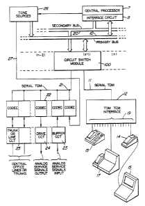
In Figure l a digital key telephone system provides for
connection Gf various digital telephone instruments, as
exemplified at 13 and 14, and various digital data terminals,
personal computers or the like, as exempli-fied at 15 and 17~
which are able to communicate, via the system, with one another
19
, ~ . .
, .
., ~ .:, : i , . . .
.. ., , , , :
... .: ~:
, . : : :
. :: .
~32~
as appropriate, and with other devices via line or trunk circuits
23. The lines and or trunks serve to connect the digital key
telephone system w-ith o-ther telephone Facilities, -For example a
central office or private exchange (not shown~. A back bone of
the digital key telephone system is provided by a short parallel
time division multiplex (TDM) bus 10, which provides a wide band
communication path between up to nine ~4 channel circuit switch
modules 100, a central processor interface circuit 8 and tone
sources 26. If any of the tone sources 26 provide an ana`log
signal, such is coupled into the system via a lead 27. The bus
lO is referred to as a primary bus, and a secondary bus 20,
similar to the primary bus 10, provides ~or untdirectional
communications from the interface circuit 8. Each of the circuit
switch modules 100 couples 64 ten bit transmit serial channels
to predetermined corresponding time slots in the bus lO, and up
to 64 parallel selected TDM time slots on either of the buses lO
or 20 to 64 ten bit receive serial channels. Thirtytwo of the
serial transmit and receive channels are coupled to an internal
ports circuit l2 via a serial TDM path 11. The remaining
thirtytwo serial transmit and receive channels are coupled to
external port circuits at 22 via a serial TDM path 21.
Each of the channels is capable of transmitting a binary
signal pulse stream at a rate of 80 kilo bits per second, with
at least 64 kilo bits per second being a~ailable as a channel for
pulse code modulated (PCM) voice information, or data
in~Formation. The remaining sixteen kilobits may be co~mitted to
supervisory and signalling communications, in association with
the PCM or data information. In this example the internal ports
. .
- ~ . .
~ ,., ~ , . .
. ~: :. , :., : .
~32239~
circuit 12 consists of sixteen TDM time compression multip~lex
(TCM) interfaces. The TCM method o~ signal kransmission is
sometimes referred to as "Ping Pong" transmission. Each of these
interfaces provides a transmit path between each of TCM links 19
and two predetermined and fixed serial TDM channels in the serial
TDM path 11. In a similar manner analog signals are interfaced
to and From various circuits shown at 23, 24 and 25, via the
serial TDM path 21 and the external ports 22 provided by CODEC
circuits. Alternatively, it may be advantageous to provide an
external TDM port for interFacing with another telephone facility
via a digital signal transmission link, T1 or DS30 for example.
However, in this case, each CODEC circuit interfaces with a
predetermined and fixed transmit and receive channel pair of the
serial TDM path 21. Hence, for each and every port, ~that, is a
place where a di~ital telephone instrument or other digital
device or a d-igitally interfaced or compatible line, trunk and
the like may be connected to the digital key telephone system),
there is at least one predetermined -ten bit parallel time slot
in the primary bus 10 which is allocated to receive inFormation
from such device, line or trunk. In an alternative example, the
time slots on the bus 10 correspond to such device, line or trunk
for the purpose of transmitting inForma-tion thereto. However,
such alternative example is not herein further discussed.
A central processor 7 is coupled via the interface circuit
8 to the primary bus 10 for communication via a predetermined
thirtytwo of the ten bik parallel time slots. The interface
circuit 8 may receive all ten bits of each time slot on the bus
lO. Normally, only the two bits corresponding to a sixteen
,.. . . ~ .. .. . . .
,. . ,: . :
.:
~ 3 ~
hilobit sub-channel are transFerred -from the bus 10 to the
central processor 7 by the interface circuit 8, for purposes of
call control. The interface circuit 8 provides signallir)g and
supervision -From the central processor 7 via the secondary bus
at time slot occurrences corresponding to intended line
appearance destinatior1s ~ia the appropriate circuit switch module
~00. Therefore each circuit switch module lO0 transmits 10 bits
to the primary bus ~0 but receives and switches only 8 bi-ts from
the primary bus 10. The other two bits ar~ received at the
appropriate time via the secondary bus 20.
In this example, each port associated communication path
provides -For Full dupleY~ operation with two words, of ten bits
each, being exchanged every 125 micro seconds. In at least one
of -these words, bit positions 0-7 are dedicated to one of data
or voice, the bit position 8 is dedicated to signal1ing and
supervision, and the bit position 9 is dedicated to validation
of signalling and supervision. The signalling and supervision
information is collected from, and distributed to, the port
associa-ted channels via the interface circuit 8 under the
direction of the centra1 processor 7. The collected information
is gathered into by-te groupings by the interface circuit 8 -For
transfer to the central processor 7 and by a samewhat
complementary function, information is distributed from the
central processor 7~ via the interface circuit 8 into bit
position 8 of a selected one of the channels or of all the
channels.
The key telephone system is intended ko support two
generically different types of station apparatus: one being a
.
., . . ... ::
;;: - ~ .
~ 2 ~
very basic telephone station set hereafter referred to as a
STIMULUS set or an S set, which includes a bit stream interface
device, a simple processing device, and a CODEC; and the other
being a more complex featured autonomous station apparatus which
may take the form of a proprietary key telephone set, interface
apparatus, or propriatary display telephone or data terminal.
Such instrument is referred to as a FUNCTIONAL set and such
reference is intended to indicate that the apparatus contains
some call processing instructions in the form of software or
firmware. For convenience, any station apparatus which is not
an S set is hereafter refsrred to as a FUNCTIONAL set or an F
set.
In the S set, any change in its operating state, ~or example
ON HOOK to OFF HOOK or a key depression, is communicated to the
central processor 7 via the S set processing d~vice, the bit
posit;on 8 and the interface device. This is accomplished in the
S set by a continuous (request to send RTS) assertion of "00" 1n
the bit position 8 and 9 o~ the outgoing channel, until a
validated clear to send (CTS) is received in bit positions 8 and
9 of the incoming channel. When the c-rs is recognized in the S
set a STIMULUS protocol message indicating OFF HOOK is
transmitted via the S and S bit positions 8. Thereafter, a
typical call progress proceeds by way of exchange of STIMULUS
protocol messages.
By way of exemplary contrast in the F set, a request to send
lRTS) may be generated after an OFF HOOK is ~ollowed by
sufficient telephone call dialling information having been keyed
in by a telephone user. In this case the processing device and
23
. . . . , . ,~ ;. . ~., , ~ - , . ., , ............. .,, ,-, ,
' ' . ' ; ':' . ' . ~ : , ,, . : ' :,; ,i,: ;; ~ . . : ': ': .' ' - : :-' ' ' ' :'
~32~3~
its operationa1 programming perform basic call processing and,
in addition to providing dial tone at the appropriate moment, may
also generate ring back or busy tone. The F set communicates in
a similar manner to the S set, using the S and S bit positions
8. After a CTS is received from the central processor the F set
transm-its a FUNCTIONAL protocol message.
Table 1 illustrates structural arrangements of messages of
STIMULUS protoco1 and FUNCTIONAL protocol in the KSU-to-cerminal
direction.
TABLE 1
_________________________________ __ ______________ _ :
HEADER TYPE LENGTH
BinarY (HEX)
0X000000(40H)
to STIMULUS l BYTE
OX011111(5FH) _ _
0Xl00000(60~)
to STIMULUS 2 BYTES
OXl00lll
OXl0l000(68H)
to STIMULUS MULTI-BYTE
0X101l11(6FH)
OX1l0000(70H)
to FUNCTIONAL VARIABLE
0Xlll1ll(7FH)
In the header, bit positions left to right are 7 through 0.
In particular, bit positions 5 and 4 indicate the protocol of the
message. FUNCTIONAL messages in this arrangement are indicated
by both of the bit positions 5 and 4 being asserted "1".
STIMULUS MESSAGES are indicated by at least one of the bit
positions 5 and 4 being asserted "0". The purpose of each of the
bit positions in the header is illustrated in Table 2.
24
-,
,. ,:
~ ! ~ . . ' '. .
. , " ' `,' ' ' " ~
'~ . ' . ' ~,; ' ' ... ' ~ I . ' ' ' '
/ ~
~L3223~
TABLE 2
BIT 7 6 5 4 3 2 1 _ O
PURPOSE START CLEAR PROTOCOL SECOND~Y
5 TO INFORM~TION
SEND
In the case of a hea~er being in a range of 40H - ~FH, the
header is the actual message1 the gist of which is carried in the
bit positions 3-0. In messages o~ more than one byte, the second
and subsequent bytes carry information. The quantity or number
of the information bytes wikhin a message are specified in lesser
significant bit positions of the header.
The CTS bit position indicates a clear to send message and
is only of significance when received by an F set or an S set.
Table 3 illustrates the structural arrangements oF messages
of stimulus and functional protocol in the terminal-to-KSU
direction. In this direction, bit 7 is a start bit with value
1, as shown in Table 4.
TABLE 3
_____________________ _____________ ___________________________
Header Type Length
Binary (Hex)
___________________
lOOO 0000 (80H) Stimulus 1 byte
to
1101 1111 (DFH)
______________._________ _____________________________________
1110 0000 (EOH) Stimulus 2 bytes
to
11l0 0111 (E7H)
_____________ _________________________________________________
lllO 0000 (EOH) Stimulus multibyte
to
1110 illl (EFH)
_______________________________________________________________ `
1111 0000 (FOH)Functional variable
to
111l li11 (FFH)
_______________________ ._____________________________________.
- ~,
11 ~2239~
TABIE 4
BIT 7 6 5 4 3 2 1_ 0
PURPOSE start protocol secondary information
There is no CTS bit in this direGtion, since the KSU 40
doas not wait for acknowledgemen-t from the terminal when
transmitting a message to it. Message -flow control is only for
signalling messages sent ~rom the terminal to the KSU 40.
. . Plural protocols and central processor Flow control of
messages, communicated via the S and S bit positions, permit
advantageous software architectures as illustrated in Figures 2
and 3, to be resident in a key telephone system as shown in
Figure 1. In Figure 2, a key system unit (KSU) 40 includes
common equipment 41 coupled with an S and S channel 50 via
software elements, namely a network controller 42 and a data base
manager 43. The common equipment 41 is in effect representative
of a hardware interface with khe buses 10 and 20 in Figure 1 but
also includes firmware and software resident in the central
processor 7. In this example, the central processor 7 is
provided by a 68008 microprocessor available from Motorola Corp.,
of 1303 East Algonquin Road, Roselle, Illinois, 60196, U.S.A~
The central processor 7 is arranged to support modulari~ed
software elements such as the elements 42 and 43.
The S and S channel is a message channel which is in
operational effect common to all the FUNCTION station apparatus
of the system. Exemplified are F sets 51 and 52, an automatic
call distribution (ACD) terminal 53, a system management data
retrieval (SMDR) terminal 54 and an outboard trunk unit 55 for
26
, .. . ~ ~ . .. . . , . . :
\
~32~
connection to a central office (not shown). Each of these i 5
a FUNCTIONAL apparatus which includes its own processing device
and call processing so-Ftware.
Figure 3 illustrates an example of an architecture
configured similarly to Figure 2, but for supporting STIMULUS
sets in addition to FUNCTIONAL sets. In this case, the common
equipment 41 also supports additional modulclr software in the
form of FUNCTIONAL emulators 45~ 46 and 47. These FUNCTIONAL
emulators perform, on behalf of respective STIMULUS sets 61 and
62, and a STIMULUS trunk unit 63, to make these appear to the
rest of the key telephone system to also be FUNCTIONAL sets.
Hence, in some system configurations, economy on a per port basis
is achieved. It should be noted that FUNCTIONAL elements 52-54
may also be present in Figure 3 but were omitted for convenience
of illustration.
In operation o-f the key telephone systems in accordance with
Figure ~ or 3, any F set receiving a CTS message is able to
transmit to all FUNCTIONAL entities, be these apparatus or
emulators. Likewise, F emulators are able to transmit to all
FUNCTIONAL entities but as the F emulators are softwar~ based in
the KSU 40, the previously discussed arbitration ritual of R-rS
and CTS is not required~ Any FUNCTIONAL entity which may thus
respond or act in accordance with -its own programming as
warranted by the content of the transmitted FUNCTIONAL message.
2~ Any such FUNCTIONAL message involving a STIMULUS set is
intercepted and subsequently acted upon by the corresponding
FUNCTIONAL emulator software module. This effectively results
in a series of STIMULUS messages being exchanged between the
: . , ,:: ,, , . , :
,. :,.: , ~ :
... . .... ..
- :: : .... . .
-
233 3`
FUNCTIONAL emulator and its associated STIMULUS sek via its S and
S channel. For example, S set 61 and emulator 46 exchange
messages via an S and S channel 61a.
In FUNCTIONAL messaging the message bits are distributed or
relayed to every channel occurrance in each frame. Although
STIMULUS sets or units are thus exposed to the ~UNCTIONAL
messages, the STIMULUS processor devices therein are arranged to
disregard FUNCTIONAL messages as recognized by the distinct
header as illustrated in the fore~oing tables 1 and 2. On the
other hand, STIMULUS messages are unidirectional~ Distribution
of a STIMULUS message is confined to the channel occurrence which
corresponds to a STIMULUS set for which the STIMULUS message is
destined.
Flow control of FUNCTIONAL and STIMULUS messages is
discussed from a hardware viewpoint aFter the following
discussion o~ the structure and operation of the modular circui-t
switch module 100 with reference to Figures 4-10.
In order that each of one or more circuit switch modulei~ 100
be able to transfer information from the serial TDM paths 11 and
21 to the parallel TDM bus 10 without conten-tion, a phased timing
sequencer, as shown in Figure 6, resides within each of the
modules 100 for regulating the functions of the module. ~ave
forms exemplified in Figure ~ illustrate a master frame timing
pulse occurring at a rate of 1 Khz, clock pulses numbered 0-27
occurring at a rate of i5.12 MHz and state machine timing pulses
SMO-SM10. With the switch module 100 installed in the system,
a preset start decoder 101 is connected to a hard wired location~
not shown, which provides an identity, that is a fixed four bit
-
~32239~
binary word, ID0--ID3. The combination oF the signal states of
the bits ID0-ID3 is unique for each possible switch module
location in the digital key telephone system. The preset start
decoder 101 generates a 5 bit binary word on a hus 102, in
response to the combination of bit states as shown in table 1.
A five bit counter 103 is preset by each occurrence of the master
frame pulse, to correspond to the word on the bus 102 and
thereafter is incremented with each occurrence oF a clock pulse.
An output 104 of the counter 103 is decodecl by a decoder 105
which generates a reset signal on a lead 106 with each occurrence
of a count of 19 in the counter 103. Thus with -the occurrence
of the next clock pulse, the counter 103 is reset to a count of
zero. Thus a modulo 20 countiny function is provided, which is
phased as is illustrated in table 5.
TABLE 5
CIRCUIT ID3 ID2 ID1 IDO PRESET TDM-11 TDM-21
SWITCH VALUE OF FRAME AND FRAME AND
MODULE 3US 102 TIME SLOT TIME SLOT
CORRESPONDENCE CORRESPONDENCE
0 0 0 0 0 18 0 2
1 0 0 0 1 17 1 3
2 0 0 1 0 14 4 6
3 0 0 1 1 13 5 7
4 0 1 0 0 10 8 10
0 1 0 1 9 9 11
6 0 1 1 0 6 12 14
7 0 1 1 1 5 13 15
~0
8 1 0 0 0 2 16 18
29
. .
.,.: , ~ ; `-`
:; " ` ., : :
. ~ . ... ` . , :
~L3~3~6
In accordance with the table, for example for the circuit
switch module 0, the channel zero on the serial TDM path 11 is
inserted onto the parallel TDM bus 10 in time slot zero, channel
one in time slot 20 and so on until the last channel, channel 31,
of a serial TDM -Frame is inserted into time slot 620.
Stated in other terms, each TDM path has 32 parallel ten bit
receiving channels assigned to it on the primary bus 10, and each
of these channels is separated from the other by 19 other channel
occurrences.
The decoder 105 also generates an SM0 timing pulse,
coincident with the count of 19 occurring in the counter 103.
~ shift register 109 responds to the SM0 timing pulse and the
clock pulses to generate additional timing pulses SM1-SM10 as
illustrated in Figure 4.
~eFerring to Figure 6, the time slot occurrences on the
parallel TDM bus -lO are tracked by a parallel slot counter which
includes a modulo 20 counter 111 and a modulo 32 counter 11~.
The counter 111 responds to the 5.12 MH~ clock pulses to provide
repetitive counts of 0 through 19 on Five time slot count leads
TSC 0-4. The counter 112 is incremented with each reset
occurrence in the counter 111 to provide repetitive counts oF 0
throu~h 31 on five time block count leads TBC 0-4, whereby in
combination binary signals on the TSC and TBC leads define 640
parallel time slot addresses per frame. A seria1 channel counter
Function is provided by a counter 113 which provides 32 channel
counter addresses on serial channel count leads SCC 0-4 to define
~ : :
~32239 :3
channel occurrences in the serial TDM paths 11 and 21. The
counter 113 -is incremented with each time block occurrence as
indicated by the timing pulsa SM6. All of the counters 111, 112
and 113 are reset with each occurrence of the Master frame pulse.
The convertar circuit illustrated in Figure 7 resides within
the circuit switch module ~o and performs both serial to
parallel conversions and parallel to serial conversions for each
of the 6~ TDMT and the 64 TDMR channels on the TDM paths l1 and
21. As be-fore mentioned, the TDMT channels are incoming and
carry data or voice, plus signalling bits originating at the
terminal instruments, while the corresponding TDMR channels are
outgoing, each to the originating terminal instrument. Each
incoming time slot includes 10 binary bits which are converted
directly to parallel form and asserted during the predetermined
time slot interval on the primary bus 10. Each outgoirg time
slot includes 10 binary bits which are obtained from one o~ two
sources: one source being a corresponding time slot interval on
the secondary bus 20; the other source being 8 bits from any time
slot interval on the primary bus 10, the 8 bits having traversed
the time switch, plus 2 bits from the time slot interval on the
secondary bus 20 corresponding to the TDMR channel occurrence.
The converter circuit is d-iscussed in more detail with
reference to the timing signals illus-trated in Figure 8. A SYSTEM
CLOCK waveform shown a-t the top of Figure ~, and some of the
o-ther waveforms in Figure 8, are idealistically depicted for
convenience as having vertical rise and fall portions. Actually,
in practice these waveforms have sloped rise and fall portions
similar to those waveforms -illustrated in Figure 4, which are
.
,,~ , .
.
.
~ 32~3~
more realistically depicted. The converter circuit, in Figure
i, includes three orthogonal shift registers shown at 501, S02
and 503 respectively. These three regis-ters perform the required
serial to parallel, and parallel to serial conversions~ Each of
the orthogonal shift registers 501, 502 and 503 is associated
with a clock generator, not shown, which produces non~-overlapping
timing si~nals, illustrated in Figure 8, for shifting and
directional control. Vertical direc-tional control signals V1,
V2 and V3 are used to vertically direct shift functions of the
register 502, 501 and 503 respectively. Horizontal directional
control signals H1, H2 and H3 are used to horizontally direct
shift functions of the registers S02, 501 and 503. The actual
loading of D type flip flop elements in the registers 502, 501
and 503 is clocked by signal pulses S1, S2 and S3. The control
signals V2 and V3 are shown in broken line to indicate that these
signal pulses are 20 system clock periods removed from the
adjacent H2 and H3 signal pulses, such that each commences at 40
system clock -intervals.Bits of the TDMR serial bit streams are
timed to be coincident with the rising edges of a serial digital
loop clock signal C690. Bits of the TDMT serial bit streams on
the paths ll and 21 are sampled and re-timed to likewise be co-
incident, by latches 511 and 521. A half cycle of the system
clock prior to the rising edge of the serial digital loop clock
signal C690, contents of the (2 by 8) outgoing register 502 are
selected by a receive multiplexer 535 to provide the first bits
of each of the TDMR channels at 11 and 21. The receive
multiplexer selection is in response to a MUX SEL OUTGOING
control signal shown in Figure 6. The outgoing bits are timed
;,
~32~3~
by the rising edge of -the clock signal C690 to start transmission
of a 10 bit time slo-t. Shortly thereafter, the starting bits of
the corresponding TDMT channels are sampled by the latches 511
and 521 using the falling edge of the same clock signal C690.
The sampled bits are then applied (2 by 2) -to t,he incoming
register 501. During -the said same clock signal C690, contents
of the register 502 and the incoming register 501 are asserted
in parallel by a multiplexer 532 on the leads of the primary bus
10. Only in an instance of a time slot (TS) 1~ occurrence, which
is indicated by a rising edge of a decode 18, in Figure 6, will
the multiplexer 532 gate Z bus signal states to the P bus 10.
A half cycle of the same system clock siynal after the falling
edge of the said same C690 clock signal, the -three orthogonal
registers 501, 502 and 503 are clocked, resulting in the incoming
register 501 accepting said starting bits, the outgoing register
503 moving the second outgoing bit to the multiplexer 535, and
the register 502 moving 8 bits of the TDMT path 21 toward the
multiplexer 532. At the same time the incoming register 501
rnoves the remaining two bits toward the multiplexer 532 via a
multiplexer 533. The next two outgoing parallel information
bytes are moved through data holding registers 504 and 505, under
control of timing signals SM2 and SM6 and hence1 into the
register 502. At the same moment, as before described, the
register 501 stores the first two bits of each incoming TDMT
channel. Once the -first two bits have occurred, the registers
501 and 503 receive no further clock signals until the start of
the next outgoing time slot sequence when all 10 regis-tered bits
are shif-ted in parallel toward the P bus 10.
33
: - . . .
322~ ~
At the start of the next time slot sequence, registers 501
and 503 are caused to move their respective contents ~2 bits)
vertically, tha-t is upwardly in Figure 5. Thereafter the next
eight TDMT bits are shif-ted vertically into the register 502 and
5the previous contents are likewise shifted out; to be transmitted
via the multiplexer 535 and the T~MR paths ll and 2i. The
horizontal directional control signals and the vertical
directional control signals continue to be alternately asserted
thereby repeating the parallel to the ser-ial and serial to
lOparallel cycle for each TDM channel on TDM paths 11 and 21.
The time switch circuit in Figure 9 provides for a timely
transfer of 8 information bits from one of the 6~0 time slots on
the primary bus 10 to a parallel T bus input of the parallel
input multiplexer 506 of the converter circuit in Figure 7, and
15thereby ultimately to a TDM path (ll or 21) time slot, as
directed by the central processor 7. The information bits of
each time slot on the P bus 10 are momentarily captured by a data
input latch circuit 710 and thereafter applied at an input 702
of a dual port random access rnemory (RAM) 701. The dual port RAM
20701 includes an output 703 which drives a T bus 770 in response
to a six bit adcdress applied at a read access address port 704.
The RAM 701 differs from a typical dual port memory device ;n
that for the purpose of storing information received at its input
702, it does not include the typical address decode circuitry.
25Instead, each write address is decoded and applied to an
individual one uf 64 write enable leads at 706. The decoded
write address is timed via a write enable latch ancl strobe
circuit 720. Any number of the write enable leads may be
34
~2~3~ 3
asserted by the circuit 720 simultaneously. The dual port RAM
701 responds, to a signal assertion or signal assertions on any
or all of its 64 write enable leads at 706, by storing -the signal
states o~ said 8 int`ormation bits at the corresponding memory
location or locations as the case may be. For example, if none
of the leads at 706 is asserted, no storage locations are
written. I~ one or more of the leads at 706 is asserted, the one
or more corresponding storage locations are written. Reading of
the 64 dual port RAM storage location occurs sequentially on a
regular and periodic basis, under the control of a flip flop, not
shown, in the latch 711 which is toggled by signals SM2 and SM6,
and the 32 sequentially generated TDM channel addresses which are
generated by the counter 113 in Figure 6.
A connection memory 730 contains information as to the actual
time slots of the 640 P bus lO time slots from whence information
bit states are stored in the dual port RAM 701. The connection
memory 730 is provided by a content addressable memory which
includes an elaven bit data input port 731, a six bik address
port 732 and a 10 bit compare address port 733. The general
structure and operation of content addressable memories is known.
In this example P bus addresses, from whence in~ormation is to
be stored, are lodged in memory locations in the connection
memory 730. Each of 64 memory locations, not shown, correspond
with a separate one of 64 output leads at 736. A digital
comparator, not shown, is associated with each o~ the 64 memory
locations such that addresses appearing at the compare port 733
are each compared with the information stored at each of the 64
memory locations. In every instant where the address at the
: . . .,: : , .
"
, ~ , ......... . .
, . . , : ~: :
32~9~
compare port 733 and the -information at a memory location is the
same and the memory location also includes an asserted validity
bit the corresponding one of the 64 output leads at 736 is
asserted. The asserted s-tate is eventually transferred via the
circuit 720 to the dual port RAM 701 which responds as
previously described.
Operation of the circuit switch modules 100 is directed by
the central processor 7 which uses the interface circuit 8 and
32 dedicated time slots on the P bus 10 for lodging information
into the memory locations of the connection memory 730 via a data
latch circuit 740 and an address latch circui-t 7~0. The
information is delivered from the interface circuit ~ in the form
of -Four bytes each of which occupies time slot l~ of 4
sequ0ntially occurring time blocks on the P bus 10. The four
l~ bytes include a command byte followed by an address byte a low
order data byte and a higher order data byte. Each of -these
bytes is asserted along with a validity signal on one o-f the two
remaining leads of the P bus 10 which indica-tes that the bytes
are in fact an instruction ~rom the central processor 7. A
portion of the command byte specifies either a write or a read
function intended for one of a connection memory a source
connection memory or a destination connection memory. A
comparator responds to the validity signal and a match between
a remaining portion of the command byte and the IDO-3 by causing
2~ the address latch -to store the next byte~ that js the address
byte. Therea-fter the da-ta latch 740 in Figure 9 captures 11
bit states of the low and higher order bytes which are
subse~uently stored in the memory location of the connection
36
,, "
~1 322~3 3
memory 730 as indicated by six address bits asserted by the
address latch 750. Provision is also made for the central
processor 7 to confirm the information content of any address in
the connection memory. In this case the command byte indicates
the read function, and the address byte inclicates the memory
locatior~ to be read. The subsequent low and higher order bytes
are driven by the stored information from a data output 738 o-f
the connection memory 730 ar,d via an output latch 7i2 and buffer
713 to the Z bus and thence via the multiplexer 532 in Figure 7
onto the P bus 10 where it is picked up by the interface circuit
The time switch conference circuit in Figure 10 provides a
three party conFerence feature in the digital key telephone
system. The time switch conference circuit adds an ability for
a timely transfer of 8 information bits from another o-f the 640
time slots on the P bus 10, ultimately to, for example, said TDM
path tirne slot previously referred to at the beginning of the
discussion of Figure 9. Very briefly by way of introduction,
bytes are presented to a multiplexer 992, in Figure 10, via the
T buses 770 output from Figure 9 and via a conference C bus 991.
The four most significant bit (not including the sign bits) of
each byte are compared in a comparator 993 which directs the
multiplexer 992 to assert the 8 bits from the C bus 991 on the
T bus 540 in the event that the value of the ~ hits from the C
bus 991 is equal or greater than a value of the ~ bits from the
T bus 995. In the event the T bus 995 value is greater, then the
8 bits ~rom the T bus 995 are asserte~ on the T bus 540 by the
multiplexer 992. Thus a three party conference call may be
37
.
. ;,
. . "
'
~3`~
implemented wherein each party hears only the instant loudest
speaking party o-f the other two parties.
Considering the time switch conference circuit of Figure 10
in rnore detail, the information bits o~ each time slot on the P
bus 10 are momentarily cap-tured by a PCM input latch 910 and
thereafter applied at an input 902 of a dual port RAM 901. The
dual port RAM 901 includes an output 903 which is buffered to the
C bus 991 via a PCM output la-tch circuit 990. Likewise the T bus
770 is bu~fered to the T bus 995 via a latch circuit 994. The
dual pork RAM 901 differs from the dual port RAM 701 in that it
has only 16 memory locations and lacks typical address decode
circuitry for the purpose of reading out information stored at
these memory locations. Each write address is decoded and
applied to an individual one o-f 16 write enable leads at 906 and
likewise each read address is decoded and applied at an
-individual one o-f 16 read enable leads at 907. The decoded write
address is timed via a write enable latch and strobe circuit 920.
Likewise the decoded read address is timed via a read enable
latch and strobe circuit 970. The read enable latch and strobe
circuit 970 also includes an EXCLUSIVE OR logic circuit not
shown, which responds to a single decoded read address occurrence
by asserting a compare enable signal on a lead 971. The compare
enable signal is used to activate the selection function of -the
comparator circuit 993, which in the absence of the compare
enable signal causes the multiplexer 992 to assert the T bus 995
bit states onto the T bus 540, exclusively. Hence if no decoded
read address or more than one decoded read address is asserted
at inputs of the read enable latch and strobe circuit 970, the
3~
- , : , . ~: : :~ --. : .: : :
~ f3 ~'~
conrerence function does not occur. The dual port RAM 901
responds, to a signal assertion on a write enable lead at 906,
by storing the signal states o-F said 8 information bits at the
corresponding memory location. Likewise, reading of a mamory
location in the dual port RAM 90l occurs in response -to a
corresponding read enab'le lead at 907 being asserted.
A source connection memory 930 contains information as to the
actual P bus time slots -from whence information bit states are
stored in the dual port RAM 901. The source connection memory
930 is provided by a content addressable memory having 16 memory
locations, not shown, each corresponding to a separate one of 16
output leads at 936. The source connection memory 930 inc'ludes
an eleven bit data port 931, a six bit address port 932 and a ten
bit compare address port 933. A digital comparator, not shown,
is associated with each of the 16 memory locations such that
addresses appearing at the compare port 933 are each compared
with the information stored at each of the 16 memory locations.
In an instant where the address at the compare port 933 and the
information at a memory location are the same and the memory
'location also includes an asserted validity bit, the
corresponding one of the 16 output leads at 936 is asserted. The
asserted state represents a decoded write address, which is
subsequently transferred via the circuit 920 to the dual port RAM
901 which responds as previously described.
A destination connection memory 930 contains in-formation as
to the actual TDM~ time slots on the TDM paths 11 and 21 to which
information bit states stored in the dual port RAM 901 may be
directed via the mul-tiplexer 992 and the T bus 5~0. The
39
.
: . :
, ,
:
~,
! ' ''
. .
~22~ ~
destination connection memory 980 is o-F a struc-ture similar to
that of the previously described source connection memory 930.
Addresses appeari~g at a compare port g83 are each compared with
information stored at each of 16 memory locations. In an instant
where the information at the compare port 983 and the information
at a memory location are the same and the memory location also
includes an asserted validity bit, a corresponding one o-F l~
output leads at 986 is asserted. The EXCLUSIVE OR logic circuit
in the read enable latch and strobe circuit 970 permits the
corresponding read enable lead a-t 907 to be asserted, which
causes the dual port RAM 901 to read out the 3 information bit
states from the corresponding memory location as previously
described.
The information appearing at the compare port 983 is asserted
frorn the channel counter bus leads SSC 0-~ by a channel counter
latch circuit 911. The latch circuit 9l1 also includes a flip
flop, not shown, which is toggled by the -timing signals SM2 and
SM6 and thereby provides 6~ addresses per frame, similar to that
previously discussed in relation to the latch circuit 711.
Operation of the conference function in -the digital key
telephone system is directed by the central processor 7, which
uses the interface circuit 8 to communicate with-the 32 dedicated
time slots on the P bus 10 for lodging information in-to the
memory locations of the source connection memory 930 and the
destination connection memory 980 via a data latch circuit 940
and an address la-tch 950 in a manner similar to that previously
discussed in relation to the connection memory 730. Likewise the
central processor 7 may con-firm the in-formation content of the
~0
- ; ~ :: ,. . ,:,, :. :
, , . , : : ~ . .: ,
,;:, , ., : :. . ::
, ,- , - : ~ :
~, - , , ,. . ,, - ,. :~
2`~
source connection memory 930 by way o-f a data output 938, a data
output latch circuit 912, a buf-fer circuit gl3 and the Z bus,
connected as shown in Figure 8. Information content of the
destination connection memory is also available to the central
processor 7 by way o-f a data output 9~, a data output latch
circuit 914, a bu-ffer circui-t 915, and the Z bus, connected as
shown in Figure 10.
A primary function o-f the interface circuit 8, as illustrated
in Figures 11 and 12, is that of receiving S and S messages and
distributing S and S messages. The S and S messages are received
from the primary bus 10 in one port related time slot at any one
time by S and S receive bu-ffer registers 810. The S and S
messages are transmi-ttecl to all of the secondary bus 20 time
slots or to a selected one of the secondary bus 20 time slots by
S and S transmit buffer registers 820. The S and S messages are
physically coupled with the primary and secondary buses 10 and
20 by a bus buffer circuit 801. The interface circuit is
similarly coupled to central processor address and data buses,
a-t ~98 and 899, by a processor buffer 805. A primary function
of the buffers 801 and 805 is that of relaying signals between
all of various potential signal sources and destinations while
minimizing the actual number of receiving gates and driving gates
physically attached to the bu~ses and various unillustrated timing
and control leads. Provision o-f such buffers is usual in digital
electronic systems and does not warrant detailed discussion.
Another primary -function of the interface circuit ~ is that
o-f capturing requests to send (RTS) an S and S message~ As
be-fore described, an RTS occurrence is marked by '~ero'
41
~.
.-. ~
,: , , . , ; : :'-
:. . . . ..
.~
,
"
~3~2~
occurrences in bit posit-ions 8 and 9 in a time slot. A valid
siynal detector receives each bit 9 time slot state and detects
and latches the 'one' state for a short time. A request to senci
detector 816 likewise receives each bit 8 time slot state. If
the valid signal detector 815 is unla-tched and the bit 8 state
is 'zerol, the RTS detector 816 asserts a request to send signal
indication on an RTS lead 816a. If the request to send is from
within a selected group of time slots, a receive shift clock
(RSCL) causes a shift register portion of the buffer registers
810 to shift the RTS indication into the buffer register 818.
After sixteen RSCL pulses, a receive load clock (RLCL) causes the
contents of an intermediate two byte shift register to be
transferred to a two byte output register. The contents of the
output byte register are available at the processor buffer 805
via an S and S rnessage bus 812. Thus the registers 818 are
clocked to monitor a group of 16 specified ports in the key
telephone system for RTS occurrences. An occurrence of an RTS
during any input from any of the 16 specified ports is arranged
to generate a low level interrupt to alert the central processor
to the presence of information. However, as it is intended that
each port connected apparatus will continuously RTS until a clear
to send ~CTS) is received by it, there is no particular urgency
attached to any one RTS occurrence. Even-tually, -the central
processor will specify transmittal o-f an appropriate CTS and
simultaneously select the port related time slot as a source of
an expected S and S message.
When a CTS message is detected in the intended station
apparatus a response, in the form of at least a one byte message,
42
., . . ~, :. :
~ 3 2 ~
is transmitted. The first bit of the message is a 'one~ in the
bit 8 position and a valid ;one' in the bi-t 9 position. This
combination causes a start bit detector 817 to raise a start bit
(SB) signal for the duration of subsequent uninterrupted valid
signal detection occurrences, coincident with the selected time
slot. In the presence of the S~ signal, RSCL pulses (one per
frame) cause bit 8 states of the selected time slo-ts to be
shifted into-the S and S receive buf-fer registers 810. Interrupt
signals are generated with every byte so collected, such that the
central processor is able to receive and if necessary, internally
encue the incoming S and S message.
Outgoing S and S messages are received from the processor
buff`er 805 via a bus 822 as timed by transmit load (Tl~) pulses.
~ shift register in the register 820 shifts received bytes, bit
by bit toward the bus buffer 801 at a rate of one bit per frame
in response to transmit sh-ift clock (TSCL) pulses. The state of
the output stage of the shift register is continuously applied
to a transmission gate 823. For this operation, the transmission
gate 823, and an idle bit driver 828, are both responsive to a
time slot select (TSS) signal. In the case of a stimulus
message, this TSS signal is derived from a "transmit port'
register 2480 (Figure 24) which is written in-to by the central
processor 7 in dependence upon the destination port number. In
the case of an F message, the TSS is asserted throughout -the
25 length of the message continuously, frame after frame. In the
case of an S message, the TSS is asserted for the duration of the
time slot associated with the destination port of the S message.
The idle bit driver asser-ts a 'one' on the lead 829 when the TSS
43
.~ . .: " . ' '~,
31 ~22~9 '~'~7
is not asserted. A valicl si~nal driver 825 responds to the TSS
assertion by asserting a 'one' on a lead 8267 whereby S and S bit
asser-tion on the lead 82~ are accompanied by valid signal bit
assertion on the lead 826.
Another capability of the interFace circuit 8 is that of
providing wide band data paths between any o~ t;he port associated
64 Kbs channels and the central processor 7. Input is received
from any specified channel via a data receive buf~er ~30 under
the control of a read bus (RB) strobe, which is generatad
coincident with occurrence of a primary bus time slot-from which
receiving is required. This occurrence preferably raises a high
level interrupt which is intended to result in a write to
processor (WP) strobe being generated to provide the bu-ffered
byte on a bus 831 For use by the central processor 7. In like
manner, bytes of information are transferred -from the central
processor 7, via a data transmit buffer 840 to a bus 841, for
assertion during a predetermined tirne slot on the primary bus 10.
Although the buffers 830 and 840 provide a convenient data
transport interFace, this type of interface can be unduly time
consuming i~ such transfers are to occur frequently. For
example, frequent data transfers are required between the switch
modules 100 and the central processor 7, in order to exercise
prompt control of communication paths in the key telephone
system. Hence, a more specialized interface is provided which
operates throughout the 32 time slots on the primary bus 10,
which are dedicated to exclusive use by the central processor 7 7
as previously described. Connection instruction bytes are
loaded from a bus 863 -to a four byte FIF0 861 via a multiplexer
44
.. - , , , ,, :: ,.
, ,, : : :
~322~ ~
860 in the presance of a write (~l) signal. After the FIF~ 861
has received four bytas, -the central processor 7 must direct the
interface circuit to -initiate transfer of data to the circuit
switch 100 via a bus 86~ and khe primary bus lO. The -inter-Face
circuit asserts the bits states appearing at the FIFO output onto
the primary bus 10 wi-th each ocGurrence of a dedicated control
time slot. If no in-Formation -transfer is required, an idle code
is asserted on the bus 863 ancltherefore is subsequently asserted
on the bus 866. By this means, up to 32 bytes of connection
instruction can be trans-Ferred via the primary bus durinc~ each
frame. Up to 16 bytes of query and 16 bytes of response
informa-tion may be exchanged via the primary bus 10 by loading
the FIFO with a 2 byte query message.
Functional circuit blocks in Figure 12 interface with the
central processor 7 via the sarn0 processor buffer 805, shown in
Figure 11. In Figure 12, a time slot address generator 880
similar to that discussed in relation to Fiyure 5 provides
definition of -time slot interval occurrences on the primary and
secondary buses for the interface circuit 8. Particularly,
address registers 881 are selectively loaded via the buf-fer ~05
from the central processor 7 to define; those time slots which
are watched for RTS, -that time slot which is granted S and S
message transmission to S and S receive bu~fer registers 810; and
the -time slot selected for s-ingle channel transmission o-F an S
and S STIMULUS rnessage or a CTS message.
In operation, a comparator apparatus 882 monitors the
contents of the address registers 881 and the time slok address
occurrences frorn the yenerator 880. Occurrences of matches, in
. " ~ ; -
.. ,~ ,, :: :
: :.: . : :
-.
~23~ 'i3
combination with instruct-ion of central processor origin and
signals from the detectors 815-8171 are used to generate the
controlling signals in sequence and with timing as previously
discussed in relation to Figure 11. A status and interrupt
circuit B~3, monitors the progress of S and S message trans-fer,
data byte transfers, and control byte trans~ers, with reference
-to signals o~ detector and control origin, to generate timely
interrupt signals ~Ihereby the central processor is informed of
in-Formation exchange opportunities and requirements.
The commQn equipment 41 shown in Figures 2 and 3 will
include, among other th-ings, a message repaater software module
to relay messages between terminals~ As illustrated in Figure
13, in wh-ich components corresponding to Figwres I, 2 and 3 have
the sarne re~erence numerals7 a message repeater 1601 comprises
a Functional message repeater 1601A and a stimulus message agent
1601B. Functional terminals 51 and the outboard trunk unit 55
are shown connected to -Functional message repeater 16~1A by TCM
channels 19. Likewise functional emulators ~5, 46 and ~7,
respectively, are shown connected to functional message repeater
1601A by way o~ the S and S channel 50 and -to -the stimulus
message agent 1601B by stimulus S and S channels 61a, 62a and
63a, respectively. Two stimulus sets and a stimulus trunk unit
61, 62 and 63, respectively, are shown connected to the stimulus
message agent 1601B by respective TCM links 13. The ~unctional
message repeater 1601A receives functional rnessages from
functional terminals or the database manager 43 or the network
control 42 and broadcasts them to all Functional entities in the
system.
46
~ . . . : . . .
: .: .:: .
-:
~2~
The previous1y discussed difFerence between Functional
message headers in the two directions implies that a functiona1
message received by the KSU 40 central processor 7 must be
modi-fied be-fore being broadcast in the opposite direction to
other terminals. This Function is performed in the KSU 40
central processor 7 by a message repeater 1601 (see Figure 13),to
be discussed later. The stimulus message agent, however, is
capable of only point-to-point communications with the st-imulus
terminals 61, 62 or stimulus trunk unit 63, or with -the
corresponding functional emulators ~5, 46, 47.
Each of the terminals 13, 14, 15, 17 provides an in~erface
between a user and a TCM communication channel. In telephony,
this communication channel typically terminates in analog
transducers for vo-ice communication, although this is not
necessarily the case. User actions requiring interaction with
the KSU ~0 are detected and result in -transmission and reception
o~ messaging on the signalling and super~ision channel provided
by the system~
Referring to Figure 14, at the hardware level there may b~
minimal difference between stimulus and Functional terminals, at
least so Far as s-ignalling to the cen-tral processor 7 is
concerned. The distinction is confined to the terminal processor
1488. For a Functional terminal, the processor 148~ is
programmed to respond to and generate functional messages on the
signalling and supervision channel 50. In a stimulus terminal,
the processor sends and receives only stimulus messages, ignoring
any incoming ~unc-tional messages which may be present on the
47
:
~ f ,
3~239~
channel. It should be noted that these two message types are
distinguished by their unique header formats. (See Table l)
The blocl< diagram of Figure 14 represents either a functional
terminal or a stimulus terrninal. A large por-tion of the
functionali-ty of the terminal is provided in a single hardware
component the Digital Terminal Inter-face Chip (DTIC) 1470. The
functional blocks wi-thin the DTIC 1~70 inclwde a TCM interface
1475 D channel interface 1476 speech envelope detector -1478 and
codec 1480 linked by two separate buses 1471 and 1~72
respeckively. Bus 1471 is a parallel bus that accesses data
reyisters via a processor interface 1473. These registers are
resident in each of the functional blocks and allow a processor
off the chip to control and obtain status specific to that
functional block. The second bus 1472 is a synchronous serial
bus carrying signalling and supervision channels and
cornmunication channel data in a format similar to TCM.
A terminal hardware identifier 1474 comprises an Erasable
Programmable Read Only Memory (EPROM) to s-tore a digital
identifier that is unique in the system. In this example the
identifier 1474 is a 40 bit code that may be written to the
device once only after completion of manufacture.
This identifier 1474 may be read by the terminal processor
1488 via a terminal processor interface 1473.
The signalling and supervision channel and the communication
channel are combined and put into a Time Compression Multiplexed
digital format. The TCM interface 1475 performs the multiplexing
and demultiplexing of these channels for transmission to and
reception -from the TDM TCM interface 12 in the KSU 40 by way of
48
. , ., ~ ~ , . , ;, ,
, ,." : . ,
, : . : : . -: - ~ ::. .
, . . . ~ : : :::
`3 ~ ~
an an~log interface circuit 1495 which provides ampli-Fica-tion and
bufFering. TC~I inter~ace 1475 dekects absence of the TCM signal
transmitted from the KSU 40 and records this status in a statws
register 2300 (Figure 23) readable via the processor interface
!473. This allows the terminal processor 1488 to detect
connection of the terminal to the KSU 40.
T~e signalling and supervision channel is known as the D
channel portion of the TCM frame. The D channel interface 1476
receives both stimulus and functional messages originating -From
the KSU 40 and formats them for the processor inter-face 1473.
Messages originating from the processor 14881 to be transmitted
to the KSU 40, are formatted for the TCM frame. In addition, D
channel flow control protocol (clear to send CTS/request to send
RTS - see later) is handled by D channel interface 1476 as
discussed previously.
A speech envelope detector 1478 is provided as part of local
voice signal processing used in performing a handsfree function
in khe terminal. Also, a combined analog to digital encoder and
digital to analog decoder (codec) 1480 is included -to provide
voice communication.
Various analog inputs 1482 are provided for voice
communication, such as a handsfree microphone~ handset microphone
or headset microphone. Various analog outputs 1484 such as for
a loudspeaker, handset transmitter or headset transmi-tter, are
also provided. Amplification and level control oF these analog
signals is provided, as well as switching of the analog inputs
and output between these various transducers ~y an analog
interface 1486. In additlon, audible user indications such as
49
",, ~: .
3 ~ 5
toMes and a ringing signal are generated by the analog inter-~ace
1486.
User input to the terminal is detected as key depressions
that close switchas in the key matrix 1490 and result in input
signals to the processor 1488. The technique For detecting these
key depressions is widely used in many types of electronic
keyboards. The processor 1488 reads the key matrix rows at
regular time intervals for these inputs, while simultaneously
generating an output signal sequentially on each o-F the matrix
columns.
Visual indication to the user is provided by liquid crystal
display (LCD) indicators driven by LCD drivers 1492. The skate
of th0se indicators is controlled by the processor 1488 in
response to user actions and incoming messages.
A liquid crystal display module 1494 provides visual
representation of text to the user of the terminal. Characters
are written to this module by the processor 1488 using a common
8 bit code such as ASCII. Text may be contained in -incoming
messages, or may be generated locally by the terminal processor
1488. In this example, the display module 1494 can display two
lines of 16 characters.
The terminal processor 1488 is a general purpose
microprocessor. For both stimulus and functional terminal
apparatus, the so~tware executed by the processor 1488 is
responsible for decoding and encoding incoming and outgoing
messages, respectively, on the signalling and supervision channel
50, responding to hardware inputs 1473, 1490, 1~94. generated in
the terminal, and driving hardware outputs 1473, 1492, 1494.
:., i .. .
~2~3~
For a stimulus terminal 61 the processor 148a is a Mitsubishi
50743 single chip microcomputer, with software contained in Read
Only Memory (ROM). This software encodes user events and
terminal s-tatus into outgoing stimulus messages, and decodes
incoming stimulus messages to drive the user indicators. ~t also
provides local control o-F terminal hardware.
For a functional terminal, the processor 1488 typically has
more processing power, and a larger address space. Since the
software must provide ~unctionality equivalent to tha-t of the
funckional emulator 45 in the KSU 40, a processor such as the
Motorola 68008 used in the KSU 40 is suitable, with separate
hardware devices ~or memory and input and output. Thus a
~unctional terminal ~1 has a higher hardware cost than a stimulus
terminal 61 o-F equivalent user interface functionality.
Figure 21 illustrates data ~low within the functional
terminal 51's so~tware, which comprises both data and processing
components.
External inputs are functional messages received by way of
the signalliny and supervision channel 50, and local inputs from
terminal hardware 1473, 1490 and 1494, respectively. Hardware
inputs include transducers to detect user actions, and registers
to provide access to the status o~ hardware subsystems in the
terminal.
Outputs are directed to hardware outputs 2132 and S and S
channel 58. Hardware outputs 2132 give audible and visual
indications to the user via terminal hardware 1473, 1~92 and
149~, and provide control of hardware subsystems in the terminal
via-terminal components 1473 and 1494. Operational data in table
.. . ~ .
.. ... . "
, :, ~: :
. . : :. ~ : : : .:, : : ::
-
~ 3 ~
1611 maintains a record of interac-tions between the -terminal and
other functional entities in the system. This data -is updated
in response to functional messages sent to and received by the
terminal.
Adminis-tration da-ta in table 1612 records the settings of
terminal specific parameters tha-t control the behaviour of the
terminal. The terminal also includes local cc,pies in table 1612
of syst.em and terminal specific administration data maintained
by -the database manager~
~0 Incoming functional messages are received by the terminal
over the si~nalling and supervision channel 50. These messages
provide information regarding the activity of other functional
entities in the system. Outgoing functional messages are
generated by the terrninal in response to local hardware inputs
and received functional messages. These messages provide
interaction wi-th other- functional enti-ties in the system. The
processins components of the funct-ional terminal are partitioned
to deal with the two specifi G types of inputs: hardware and
functional rnessages~
The hardware inpu-t handler 2135 updates internal data ancl
generates both messaging and harclware outputs. It responds to
local user inputs, and status changes detected in hardware
subsystems.
Figure 22 illustrates da-ta flow within the functic,nal
2~ terminal emulator software. Each func-tional terminal emulator
45 has a functional message handler 2220 and a stimulus message
handler 2222. The functional message handler 2220 upda-tes
internal data and generates both functional and stimulus
~2
' ~ . ~, . , ' ! . : '.
, ~' '.,' : . ~,
~322~
messaging. I-t responds to functional messages received -From the
signalling and supervis.ion channel 50.
To a large extent, the data flow within the functional
emulator ~5 is identical to that of the functional terminal 5l.
The key distinction is that direct hardware inputs 2131 and
outputs 2132 are replaced by incoming and ou-tgoin~ stimulus
messages, 2225 and 2226 respectively, on the signalling and
supervision channel 61a.
With the exception of stimulus messages replacing hardware
data, the functional emulaior data components are substantially
identical to those of khe functional terminal 51. Since multiple
funotional emulators are implemented on a single shared processor
in the KSU 40, the organiza-tion o-f operational and administration
data components of the functional emulator 45 diFFers From their
organization in the Functional terminal 51. This organization
within -the KSU 40 was illustrated in Figure l9B.
Incoming s-timulus messages are originated by the physical
stimulus -terminal 61, and indicate user actidn or terminal
status. There is a one to one correspondence between a
functional emulator 45 and a physical terminal 61, and the
stimulus messages 2225 -frorn a stimulus terminal 51 are handled
exclusively by one 1Functional emulator 45.
Outgoing st-imulus messages 2226 are generated by the
functional emulator 45 to update audible and visible user
indicators at the physical s-timulus terminal 61. The -Functional
emulator 45 generates stimulus outputs 2226 -for one stimulus
terminal 61 exclusively.
53
:, . :,
~322~
The hardware input handler of the functional terminal is
replaced by a processing component, stimulus message handler
2222, to handle incoming stimu'lus messages 2225 in the functional
emu'lator ~5. The Functiona'l message handler 2220 is
5substantially identical in both the functional terminal 51 and
functional emulator 45.
The stimulus message handler 2222 updates internal data and
generates both Functional and stimulus messaging. It responds to
user inputs and stimulus terminal status, reported in incoming
10stimulus messages 2225.
At the software level, signalling and supervision message
flow diFFers for functional and stimulus messages even though
both message types share a common physical channel at the
hardware level This distinction is possible at the software
15level due to the d-istinct headers oF the two message types. At
the hardware le~el message Flow is identical for both stimulus
and functional messages.
At the hardware level, messages are transmitted From, say
terminal 13 to the central processor 7 (Figure 1~. Within the
20terminal 13 are the hardware components shown in Fiyure 14
including the processor 1488 which writes a message into its
memory, for example in rèsponse to a user action such as a key
depression detected in the key matrix 14gO. The processor l488
copies this message one byte at a time into a "transmit data"
25register 2301 in the D channel interface 1476 via the processor
inter-Face 1473 (see Figure 23).
Following RTS and CTS flow control handshaking with the KSU
40, the TCM interface 1475 inserts the message bits into the TCM
5~
~22~ 3
frame on -the TCM loop 1496. Once the D channel interface 1~76
is ready to accept the next byte of the message, -the ~TIC 1470
signals the -terminal processor 1488 with an interrupt. The
processor 1488 then writes the next byte of the messag0 into the
"transmit data" regis-ter 2301 in the D channel interface 147S.
Terminal 18'5 TCM loop is time division multiple~ed with
other T~M loops by the TDM TCM interface 12 in the KSU 40. The
message then passes via the serial TDM link 11 and the circuit
switch module 100 onto the primary bus 10, where the S and S
channel bits are collected by the interface circuit 8. Once a
byte of the message is assembled, processor 7 reads the message
byte from a "receive data" register 2478 (Figure 2~) in the
interface circuit 8. In addition, the port number of the
terminal originating the message is read by the processor 7 from
the "receive port" register 2479 in the interface circuit 8. In
response to subsequent interrupts from the interface circuit 8,
the processor 7 buffers subsequent received bytes from the
~'receive data" register 2~78 in memory until the entire message
is received. Sof-tware in the processor 7 then e~amines the
message and -ta~es appropriate action. The data registers 247a
and 2481 will correspond to registers 810 and 820, respectively,
in Figure 11. The port registers 2479 and 24~0, respectively,
will be connected in a similar manner.
For message transmission from the KSU ~0 to, say the terminal
13, the reverse process is followed. Software in the central
processor 7 writes an outgoing message into a block of memory.
Before transmission of the message begins~ a "transmit port"
register 2480 ~Figure 24) in the interface circuit 8 is written
: ~: :: :............... : .- .: : : :
. . ~ , . ., . .. .: ::
~2~3~ 3
by the message repeater 1601 specifying the port on which the
message is to be sent. The message may be sent on one port, only,
or on all ports simultaneously (broadcast). The message is
written one byte at a time by the message repeater 1601 (Figure
16) to a "transmit data" register 2481 in the interface circuit
a. The interface circui-t 8 writes message bits to the secondary
bus 20 with the appropriate timing. When it is ready for the
next byte o-f the messa~e, the interface circuit ~ interrupts the
central processor 7. The central processor 7 responds to this
in-terrupt by writing the next byte of the message to the
"transmit data" register 248l in the inter-Face circuit 8. The
message bi-ts appear at the TCM loop l9 connected to the
destination terminal 13 after passing from the secondary bus 20
to the circuit sw-itch module lOO, and via the serial TDM link 11
and the TDM TCM in-terface 12.
Within the terminal 13 shown in Figure 14, the message bits
are passed through the TCM interface 1475 and collected via the
D channel inter-face 1476 after a "start" bit is recognised in
interface 1476. Once a complete byte o-f a message is assembled,
the DTIC 1470 interrupts the terminal processor interface l473.
The processor 1488 reads the message byte from the "receive data"
reyister 2302 (Figure 23) in the DTIC 1470. The processor 1488
reads subsequent message bytes from the "receive data" register
2302 i n response to æubsequent interrupts from the DTIC l470.
So-ftware in the terminal processor 1488 then examines the message
and takes appropriate action.
Stimulus messages are buffered separately from functional
messages in memory in the KSU 40 central processor 7. For
66
- , ~ : , ::, . ... .. . .
~3~2~
messages received from terminals, khe message repeater 1601
examines the header byte of the incoming message and selects th0
buffer. For outgoing messages~ the software generating the
message chooses the appropriate buffer based on the message type.
For both incoming and outgoing messages, the source and
destination por-t numbers are included in the buffer.
Stimulus message flow at the software level is exe~plifed in
the sequence of initiali~ation messages in Figure 18.
When a stimulus terminal is transmitting to the KSU 40, a
pointer to a received s-timulus message is passed to a single
-functional emulator 45 via a procedure call, providing access to
the S and S channel 61a by the functional emulator 45, in the
terminal-to-KSU direction. This message is processed by the
stimulus message handler 2222 (Figure 22).
For signals transrnitted -from KSU 40 to a st-imulus terminal,
outgoing stimulus messages are genera-ted by the functional
emulator 45 by internal processing components stimulus rnessage
handler 2222 and functional message handler ~220 (Figure 22).
These messages are placed in the appropriate buffer memory in the
KSU 40 central processor 7, af-ter which they are transmi-tted to
a single TCM port.
Examples of functional message-flow at-the so-ftware level are
illustrated in Figures 17 and 18.
Within the KSU 40 processor 7, software passes a poin-ter to
a rec~ived functional message via a procedure call to functional
entities such as 42, 43, 45, 46 and 47 within the KSU 40
sof-t~are, to provide a virtual S and S channel 50 within the KSU
40. Each -functional message is passed to each -functional entity
~7
.. . :
3 ~ {i
ln the KS~J ~0, in order- to provide the equivalent of broadcasting
on the physical S and S channel external to the KSU 40. Within
the -functional emulator ~5,the functional message handler 2220
processes the incoming message.
Outgoing functional messages, generated by f-lnctional
entities such as 42, 43; 45, 46 and ~7 within the KSU 40, are
placed in the appropriate buf~er memory in the ICSU 40 processor
7, after which they are passed both to functional entities
internal -to the KSU ~0, and also broadcast to all TCM ports.
External to the KSU 40, the functional message handler ~134
in the functional terminal software in Figure 21 processes an
incoming Functional message that has been written int~ a memory
buf~er by the functional terminal processor 1488 in F-i~ure 14.
The functional terminal software also writes outgoing functional
I5 messages to a memory buf-fer in the terrninal processor I488
(Figure 14) that are sent to the KSU 40 via the DTIC 1470.
Figure 16 illustratas the system components involved in
implementing terminal relocation or replacement and shows
multiple terminal devices 51, 52 and a functional emulator 45
which communicate with each other and with database manager 43
via the message repeater 1601. The message repeater has multiple
physical connection points or ports 1602 - 1606 and the S and 5
channel is access1ble at each of these ports. Only ~unctional
messaging is relevant to Figure 16.
Each o~ -the message ports 1602-1806 is an interface point
between the associated terminal and the rest of ~he system and
is bidirectional, i.e. messages may be both sent and received by
a connected terminal. Messages may be addressed specifically to
58
,. .
~ ;: i ,
~32~3~
o-ther -terminal apparatus in -the system, or may contain no
explicit destination address. The address oF the originating
terminal is included in the message. The relationship between
address and port number is not fixed, i.e. a terminal address is
unchanged when a terminal is moved to a di~feren-t port.
As mentioned previously, the message repeater 1601 is part
of the KSU 40, and is mainly resident in the interface 8 w-ith
some processing capability in processor 7. It includes a
-Functional message repeater 1601 (Figure 16) which receives
messages sent by individual terminal apparatus and broadcasts the
messages to every si~,nalling channel, providing the common S and
S channel 50 between -functional terminals. The message repeater
1601 can identify the port of the originating terminal uniquely,
and adds this ori~inating port number to the address information
in the message. The message, with the originating port number
included, is then broadcast by the message repeater 1601 to all
terminal apparatus in the system.
l~he database manager 43 is a KSU resident Functional entity
that communicates ~ith other functional entities in the systsm
via the signalling and supervision channel 50. In effect, the
database manager 43 is a special terminal that is permanently
attached -to the system, and is not relocatable. Thus th-is
database manager terminal 43 need not contain a unique
identi-Fier. It will be appreciated, however, that only one
database manager 43 may be present in the system. Like other
terminal appara-tus, the database manager 43 has message
transmission and reception capabilities, in this ease by means
5~
, .: : : -. . : : :, ;, . .-: .
,: i . . .. : . , . - . ..
. . ~ ~ :: ,
.. . .
3 ~ ~
of message handler 1607 which is a processing compon~nt of the
functional ent-ity.
The database manager 43 maintains a Port Map Data table
1608 which stores, for each terminal, port number, identifier
(HWid) and address or prime directory number (PDN) in a
predetermined relationship. The PDN is used as a key to okher
-t~rminal-specific data resident in the database manager ~3, and
is the number by which a terminal is identified to the user. The
PDN is analogous to the telephone number oF a telephone set in
the pub1ic telephone network. Alternatively the other -terminal
specific data may be referenced directly by HWid, or some other
unique address, rather than PDN. In addition to the "Port Map
Data" table 160~, the database manager 43 comprises "lerminal-
specific Administrat-ive Data" table 1609, and "Other Data" table
1610.
The "Port Map Data" table 1608 contains an entry for each
terminal port in the system, and the port number is used to index
the table. Each entry contains two fields: the hardware
identifier id1---idn of the terminal most recently attached to
the port, and the corresponding Prime Directory Number PDN1 to
PDNn of this terminal. This "Port Map Data" table 1608 is
updated in rasponse to "Query PDN" messages received by the
message handler 1607 of the database manager 43.
In "Administration Data" table 1609, the database manager
43 maintains administrative data specific to individual terminal
apparatus indexed according to the PDNs o-~ the terminal
apparatus. ~his data includes such information as system
..
~ ,
. . .
-" ~3223~6
controlled ~eature assignments that are not writable by the
individual terminal apparatus.
In addition to terminal specific administration data, in
table 1609, the database manager 43 maintains other
administration data, that applies system wide, in table 1610.
On each attachment of the terminal to a port in the sys-tem,
or each system initializa-tion, the terminal goes through a
process o~ internal initialization 7 which involves writing data
to initial states, and initializing states of kerminal harclware.
Thus, its internal processor 1488 sets variab'les, carries out
checks, tests, etc. turns o-ff indicators, sets hardware ports
to known sta-tes. ~hen internal initialization has been
completed, it is ready for external initialization, following
which it can begin communicating with other functiona'l entities.
Fisure 15 is a state dia~ram illustrating the ~lay in wh-ich
initial connection of the terminal is deemed to have taken place
by virtue of the fact that -frame synchroni~ation has been
established following initial physical connection or reconnection
f'ollowing a disruption which effectively constitutes
disconnection. Framing information is transferred to DTIC chip
1470 (Figure 1~) as bipolar violations embedded at a rate of
lkHz. in the BPRZ-AMl (Bipolar Return to Zero-Alternate Mark
Inversion) signal received over the TCM loop 1~96. Such a
bipolar violation is inserted in the start position of every
eighth -frame or burst of the TCM signal. The bipolar violation
is timed relative to the stop bit of the preceding burst. The
frame state machine (Figure 15) enters the out-o-f-frame mode
(state 2) whenever it misses t~lo consecutive violat-ions, and upon
61
.
' ~, . : . .
. . ,
1322~ '3
power-up or reset. It has recovered frame when, after a bipolar
violation (state 3), a second violation -is detected exactly eight
bursts later. When a violation occurs at the wrong time during
inframe mode (moda 1), it is ignored. No TCM bursts are
transmitted in out-of-frame mode. It should be noted that the
transition from state 2 to state 3 requires only a bipolar
violation, whereas the transitions From, respectively, state 3
to state 0 and from state 1 to state 0 require both a bipolar
violation and the occurrence of a stop bit in the proper
location. In order to avoid bipolar violations between
successive transmit and receive bursts, the start bit of the
transmitted burst of the DTIC chip 1470 is given the opposite
polarity to that of the previously received stop bit. This has
the affect of changing the polarities of start and stop bits at
the lkHz rate. Frame information is transferred to and from the
rest oF the system through the serial bus 1~72. tFigure 5)
As indicated in Figure 15, when the frame state machine is
in the inframe mode, a 'l' is present in the status register 2300
in TCM interface 1475. Whenever an out-of-frame conditlon
exists, a '0' is present in the status register 2300.
The processor 148~ polls the status register 2300 at regular
intervals. When it detects a transition from '0' to '1', it
presumes that a terminal has been newly-connected and transmits
the identifier signal to the central processor 7.
If the status register indicates that the terminal has been
connected, the terminal signals its presenGe to the central
proGessor 7, by sending a message to the database manager 43.
As previously mentioned, the message handler 1607 is the
62
- .. . ~ , , ~ ,,
~2`~6
processing component of the da-tabase manager 43. It receives
incoming messages and generates outgoing functional messages via
the signalling and supervision channel 50 (Figure 2), It
accesses the daka components of tables 1608, 1609 and 1610 in
response to incoming read and write request functiona~l messages.
Although, at this stage, the functional terminal 51 is
unaware o-F its own PDN, it knows the fixed address of the
database manager 43, and so can address its message properly.
For a functional terminal 51, the external initiali~ation
message sequence consists of two messages as illus-trated in
Figure 17. The first message "Query PDN (port,HWid,type)" is
originated by the functional terminal 51 and sent to the database
manager 43. `
This first message queries the PDN of the functional terminal
51. The hardware identifier (HWid) of the functional terminal
51, which is unique -in the system, and the port number on which
the message originated, are included as parameters in this
message. The "type" parameter is included by the originating
terminal to allow the da-tabase rnanager 43 to make terminal type
distinction in the terminal specific data table 1609 (Figure 16).
As mentioned previously, khe originating port number is
written into thernessage by the message repeater 1601 (Figure 16)
in the KSU 40 rather than by the originating functional terminal
51, and is included when the message is broadcast on khe
signalling and supervision channel ~0 (Figure 2). Thereafter the
functional terminal 51 will ignore all incoming ~unctional
messages except the response from the database manager 43.
63
~ his response comprises the second messaSe, PDN response
(port, HW-id, PDN,~ype~ whereby the database manager ~3 informs
the requesting functional terminal 51 of its PDN. The PDN (prime
directory number) assigned to the terminal by the database
manager 43 is included in the message. Since the terminal 51
receiving the message does not yet know its PDN, it needs some
other means o-f recogni~ing that this message is addressed to it.
For this reason, the hardware ident-iFier (H~id) is included in
the response message. The functional -terminal 51 matches the
hardware identifier ~HWid) in th0 message wi-th its own in order
to recognize itself as the destination. The functional terminal
51 then saves the PDN and port number parameters received in
the message in its operational data (1611~ in the terminal
processor l48~ (For the purpose of this description, the
operational data tables in both Functional terminals and
emulators are deemed to be the same and so have the same
reference numeral J 1611~) The terminal 51 may then ask the
database manager ~3 for other terminal specific data. In these
subsequent queries, the terminal 51 uses its own address (PDN),
rather than its identifier H~id, since the PDN is only l6 bits
long compared to 40 bits -For the identifier. Thus the HWid is
only used during initialization. Therea-Fter messaging uses the
PDN for terminal identification purposes.
Since the port number also is unique wi-thin the system, it
is included in the PDN response message.
Figure 18 illustrates the corresponding message sequence for
initialization of a stimulus terminal 61, which communicates with
the database manager 43 by way of a functional terminal emulator
~4
~ ~2 ~
4~. (see also Figures 3 and 13). The combination o-F functional
terminal emulator 45 and stimulus terminal 61 is equivalent to
the functional terminal 51 in Figure 14.
One difference between the functional terminal emulator 45
and a functional terminal 51 is that the functional emulator 45
is aware of its port number before any messaging occurs. This
allows initialization of -terminal types that do not have unique
hardware identifiers, since the functional emulator 45 can
recognize itself as the destination of the "PDN Response" message
from the database manager 43 by matching the port number.
Relocation of these terminal apparatus without unique hardware
identifiers is not supported. The PDN of these terminal types
is fixed in relation to the port.
Functional messaging between the functional terminal emulator
45 and the database manager 43 as shown in Figure 18 is identical
to that shown in Figure 17 between a functional terminal 51 and
the database manager 43 for functional terminal initialization.
However, a stimulus message sequence occurs be-tween the physical
stimulus terminal 61 and the functional terminal emulator 45
before the emulator 45 generates the "Query PDN(port,HWid,type)"
functional message.
Once it has completed its internal initialization, (see
above) the stimulus terminal 61 indicates its presence to the
functional -terminal emulator 45 by generating a "Reset
.25 Acknowledge" message. This is the first indication to the
emulator 45 that a stimulus terminal has been connected
physically to the port.
3 ~ ~
The functional terminal emulator 45 requires information
regarding the characteristics of the attached stimulus terminal
61 which may affect its operation, both during and aFter
inikialization. For example, the stimulus message meaning may
vary between terminal types, in which case the emulator 45 needs
to know. Consequently, the functional terminal emulator 45
responds with a "Query characteristics" message.
The stimulus terminal 61 responds to the query from the
emulator 45 with a "response(characteristics)" message containing
the requested characteristics. If the characteristics in khis
response identify the stimulusi terminal 61 as a type of device
having a unique hardware identifier, the emulator 45 transmits
a "Query HWid" stimulus message to the stimulus terminal 61. If
the stimulus terminal 61 is of a type which has no unique
identi-fier, no query is made and the emulator 45 proceeds
directly to exchange funckional rnessages with the database
manager 43, using a nil value for the hardware identif-ier.
Otherwise the functional termlnal emulator 45 will not commence
the functional message 1nteraction with the database manager 43
~O until the stimulus terminal 61 has responded to the "Query HWid"
message from the functional emulator 45 with a message "response
(HWid)" containing the requested identi-fier. Thereafter the
Functional message interaction between the emulator 45 and the
database manager 43 takes place as previously described.
Referring now to Figure 19, initialization will usually
result in updates to khe port map data (Figure l~ and 19A) in the
database manager 43. If the terminal is a stimulus device 61 with
.
66
. ,~:j . ~ . :. :: .
~ 3 ~
a functional terminal emu1ator ~5, emulator da-ta may also be
updated (Figure 19B).
In addition to data tables 16~8, in the database manager 43~
the K5U 40 has '`Operational Data" and "Administration Data"
tables 1611 and 1612, respectively, each row o-F the tables
accessible by one oF the functional emulators 45. The port map
data table 160~ i~ updated by the database mana!~er 4~ in response
to the "Query PDN" message (Figure 17) received from the
initializing terminal 51 or emulator 45.
Initially, the port map data table 1603 contains a "nil"
entry for the hardware identifier on each port, and a PDN that
is unique for each port. This represents the condition that
there is no terminal attached to any port. Terminal speci-Fic data
in table 1609 is initialized assuming a "default" terminal type.
16 If the type oF the terminal actually attached differs from the
de-fault, this is indicated by the "type" parameter in the "query
PDN" message. The database manager 43 then changes the data in
table 1609 to new values suitable For this terminal type.
Referring to Figure l9B, the Data Tables 1611 and 1612 in
the functional terminal emulator 45 contain emulator data that
is replicated for each port in the system i.e. each row in Tables
1611 and 161~ represents a dif-Ferent emulator. Table 1612
contains data related to operation oF the emulator 45 on the port
itselF, and Table 161l contains administration data related to
the PDN of the device attached to the port. The operational data
in Table 1612 is organized as an array indexed by port, and the
administration data in table 1611 is organized as an array
indexed by PDN. Since relocation alters the relationship between
67
.'' ',,' '``" " ' ', "'`' ~' '.'' "
.. .: " ':.: ~'; " ,' ' .~ : '
' ' '',.I .. : ,. ',',' . ' . ' ' ' '' '
' . . . ' " ' i ~ ' ; ' . ' ' ' ~ , ; ;' .
' ' ' ' ' ' , . ' " , ' ',':, , ' i', ' ', ' ., `~
,' ; ' " ~ ',:, ' '" ~ : . ", ': ,,, '
~3223~
P~N and port number, these two types of data are linked by
pointers 1613. A pointer is a commonly used type of data that
contains the memory address of other target data. When
relocation occurs, only the pointer 1613 need be modified, and
not the data itsel-~.
Initially~ the contents of the operational data table 1612
indicate that the emulator 45 is disabled, since no stimwlus
-terminal is known to be attached to the port. The admirlistration
daka in table 1611 is uninitialized, since its contents may
depend upon the type of terminal that gets attached to the port.
The pointers 1613 linking the administration data to the
"operational" or port data are initialized to corresponcl to the
PDN assigned to the port in the port map data l608.
The operational data in table 1611 will include "type" data
which will correspond to the terminal type transmitted in the
"response(characteristics)" message from the stimulus terminal
61. The adminiskration data table 1612 may then carry type-
dependent administration data. When the PDN response is received
~rom the database manager 43, the corresponding administration
data will be updated to conForm with the operational data.
There are two distinct types of initialization which require
updates to database manager 43 and emulator data tables 1611 and
1612. One is relocation, and the other is replacement.
When a new terminal, i.e. tha-t has not been initialized
be~ore in the system, is attached to a port, the hardware
identi~ier it sends to the database manager 43 in its "Query PDN"
message (Fi~uras 17 and 18~ will not be present in the port map
data table 160S, -the initial state o-F which is shown in Fiyure
68
.
- ~
~22~ ~
19(i). The table 1608 is updated by -the database manager 43 to
record the hardware identiFier (idl) at the entry for port number
(1), [see Figure 1~ ~ii)], and the PDN assigned to the terminal
is the one in the port map data column alongside that port, i.e.
PDN1. This i 5 terminal replacement.
The database manager 43 is no-t aware of a terminal 61 being
removed frorn the port and the port map data t,able 160~ remains
unchanged [Figure l9 (iii)]. The emulator ~5, however, neecls to
be aware of a stimulus terminal being removed, since it should
enter the disabled state. This allows other functional entities
to be aware of its absence, since a disabled emulator will ignore
all -functional messages. Disabliny o~ the emulator is not
essential for relocation.
Absence of the stimulus terminal 61 may be detected by having
the emulator 45 or some other KSU 40 entity, ~or example a loop
maintenance server, query the stimulus terminal 61 with a
s-timulus message at regular intervals. When the stimulus
terminal 61 fails to respond to such a query, absence o~ the
stimulus terminal 61 is indicated, and the emulator ~5 should
disable itsel~.
When a terminal that has been initialized be~ore in the
system, at a port which has now been vacated, is attached to a
new port, [Figure 19 (-iv),(v) and (vi)], the hardware identi~ier
it sends to the database manager 43 in its "Query PDN" message
2~ (Figure 17) will be present in the port map data table 160~ but
entered against the vacated port. In this case, the database
manager ~3 and emulator data tables 1611 and 1612 may be
69
,.~...... .. . . .
~322~96
updated depending on which of the following three scenarios
applies.
(i) The case of the same terminal sending a PDN query from
a port different from the port at which the hardware identifier
is stored in the port da-ta map 1608 occurs when the terminal has
relocated [Figure ~9(iv)~. The port map data table ~608 is
updated so that the entry at the vacated port with the matching
hardware identifier is swapped with the entry at ~he present port
where the terminal has now originated its PDM query. Thus in
10the example of Figure 19(iv) PDN1 is assigned to port 3 and PDN3
is assigned to port 1. The emulator data pointers 1613 are
updated to effect a corresponding reassignment o~ the
administration data for the emulators at the corresponding two
ports [Figure 19(iv)].
15(i-i) A terminal that is removed and then reattached at the
same port [Figure l9(v)~ will not result in any data updates.
This is neither replacement nor relocation but merely attachment
o~ a removed terminal at the same port.
(iii) Attachment of a terminal at a port that was previously
occupied but such that its hardware iclentifier does not match
the hardware identi~ier assigned to that port or any other port
in the port map data table constitutes replacement CFigure
19(vi)]. Database manager ~3 records the hardware identiFier of
the new terminal in the port map data table 1608 deleting the
identifier o-f the terminal that previously occupied the port.
Relocation of the previous terminal can now no longer occur. No
update to emulator data tables 1611 and 16~2 is required.
.: ,, - : ;, ~ ~ ,
., . : :
:: ,
,, ,: .. , ~ : , :. -
- ,,: , ,
~3223~
Operat-ion of the database manager 43 during the message
exchang2 is illustrated in Figura 20 wllich, like Figures 21 and
22, is a data-Flow diagram. For more information about this kind
oF diagram -for representing sofkware the reader is direcked to
chapker 10 of the book "Structured Design: Fundamentals of a
Discipline of Computer Program and Systems Design" by Edward
Yourdon and Larry L. Constantine, Yourdon Press 1978.
The database manager 43 performs two kinds of operation
following receipt of a "Query PDN" message from a functional
terminal 51 or functional emulator 45. The first operation
involves a search of the port map data table 1608, and the second
involves any necessary data updates 2024 to the table 1608.
Following these two internal operations, the "PDN Response"
message 2021 is generated. Thus, following receipt of the
hardware identifier 2019 in a "Query PDN" message from RX PORT
2025, the database rnanager 43 searches (2020) the port map data
table 1608 for a hardware -identifier ma-tching the identifier 2019
received in the "Query PDN" message. If a matching identifier
is found, a record is made of the number of the por-t with which
it i~s associated. This is the port number of the first match,
data element 2022, in Figure 20. If no match is found, the value
is nil.
The search 2020 is repea-ted through the remainder of table
l608 for a second identifier match 2023 in the port map data. If
a second match is Found, the corresponding port number(~s) is
recorded in data element 2023. If no further match is found, the
value is nil.
:.32~
Fo'llowing completion of the search, port map data table
1608 is updaked as at 2024 to reF'lect any changes due to
relocation or replacement as described in the term-inal
ini-tialization events. Decision Table 6, below, shows how the
events ars re-Flected in the values of the variables. [x = T or
F (don't care)J. The evants are numbered to correspond to Figure
19A.
TABLE 6
________________________ ______ ______________________ ____________
10 event first match second match first match result
= nil = nil = rx port
(ii) T T X replacement new set
(iv~ F T F relocation
(v) F T T replacem~nt-old set
(vi) T T X repl~c~ment-new set
error F F X replacelnent-
duplicate id
___________________________ ____________________________
Various modificat-ions and alternatives may be implemanted
without departing -From the scope of the present invention. Thus,
terminal relocation and replacement need not include source and
destination port numbers in functional message headers. The
number of the port at which the message originated may instead
be written separately into the KSU 40 message buffer by the
message repeater 1601, and be made available to the database
rnanager 43 via a procedural interface. This implies that the
database manager 43 must be irnp'lemented in so-Ftware internal to
the KSU 40. Also, it must be possible for the database manager
43 to specify the destination port number o-F the outgoin~
72
: . :, ~ :,. : : ~
- ~ "
- . . ,: : ~ . , ;
-Functional message, and allow functional emulators 45 to access
this port number to initia'lize stimulus terminals 61 without
unique HWids. In -the example described, in which port numbers
are included in functional message headers, the database manager
43 may be implemented either internal or external to the KSU 40.
It should be apprecia-ted that the port map data table 160
could be inda~ed other than by port number. It may equally well
be indexed by PDN, hardware id or some other number unique to a
port, so long as the port number is then included as an entry in
the table, and there is exact'ly one table entry for each port.
It should also be appreciated that, unlike the operational
data, the administration data in kables 1608, 1~09 and 1610 of
the database manager 43, and table ~612 in the emulator 45 and
the functional terminal 5i, are non-volatile, i.e. not lost when
power is turned off. Hence a system can be turned of-f, a
terminal relocated, and the automatic relocation procedure will
function satisfactorily when power is restored.
Relocation of a terminal involves messages initially
indistinguishable from a "Query PDN" message arriving at the
ZO database manager from a second terminal with the same HWid, i.e.
two terminals having the same HWid and trying to operate
simultaneously. This could result in the second terminal being
assigned the first terminal's PDN and data. The first terminal,
on consequent initialization, would seek -to repossess it~ The
cycle could repeat indefinitely. To avoid this situation, the
database manager ~3 prevents a second relocation of a terminal
with this HW-id -for a dura-tion of at least one polling interval
of -the loop maintenance server. On the first relocation, the
. :, ~, ~. .
~2239~
database manager 43 requests the loop maintenance server to re-
in'tialize any terminal at the vacated port via a TCM frame
violation or "rese-t`' command to the terminal. This ~orces the
terminal to send the "Query PDN" in this interval. Hence any
5 "Query PDN" message containing this HWid arriving during this
interval wili be treated as initiated by a replacement.
74
,
,
, .: