Note: Descriptions are shown in the official language in which they were submitted.
68Q6~31~ 4 1 9
FIELD OF TH~ INVENTION
This invention is related to computer networks, and more
particularly, to computer networks that transfer frames of data
through repeater nodes using elasticity buffers, and in which each
node connected to -the network is operated by an independent clock.
RELATED APPLICATION
Thls application is related in subject matter to
Canadian Patent 1,302,540 which issued on June 2, 1992.
BACKGROUND OF THE INVENTION
In the field of data communications, quantities of data
known as "frames" are often transmitted from one node (station) to
another through a network of nodes that operate using their own
independent clocks. Use of independent clocks in the nodes
requireæ a ~ystem for ensuring that data corruption will not occur
when frames are transmitted from a source node to a destination
node through a number of repeater nodes. One method commonly
employed for preventing data corruption in such networks is the
use of an elasticity buffer at each node.
An elasticity buffer is a first-in first-out storage
device including a number of single or multibit storage elements.
In the elasticity buffer, data enters and exits at different rates
corresponding to the different frequency of the cloak used in the
upstream tranæmitting node compared with t~e local clock
. . i
.
- 1 3224 1 9
frequency used in the receiving nodeO Elasticity buffers are
required even though data -transfer rates are nominally the same,
because independent clocks in separate nodes will differ in fre-
quency within some known tolerance.
An elasticity buffer is used when the incoming data rate
may vary from the outgoing data rate. The independent clocks in
different nodes are asynchronous, and at some point, data from
an upstream node (tlle sending station) must be synchronized to
the local clock in the repeater node receiving the data. Typi-
cally, incoming data is received synchronously with a transmit
clock signal of the upstream node. The transmit clock signal
may be sent to the repeater node on a dedicated clock line, or
the transmit clock signal may be recovered by the repeater node
from incoming data using a clock recovery device.
After data is received by the repeater node, some imple-
mentation~ provide that the data is first synchronized to the
local clock and then written into the storage elements of the
elasticity buffer. In these systems, data i3 written into and
read frsm the storage elements using the same local clock, and
the buffer read/write operatlons are therefore synchronous.
In an elasticity buffer with synchronous read/write opera-
tions, each data unit ~e.g.., a byte) transferred through the
elasticity buffer must first belpre-synahronized when the data
unit is received by the repeater node. For synchronous e~astic-
i~y buffers, however; metastability i~ a significant problem and
.
may result in data corruption.
-3-
., .. , . , -
1 3224 1 9
Metastability occurs when adequate setup and hold times for
input data are not provided for a logic element (e.g., a
flip-flop) that is latching in the data. In logic elements used
for synchronization, the variation in clock speeds makes the
time of arr~val of each data unit uncertain, thereby causing
errors when input data is sampled during a period of instabili-
ty. Although failure rates may be reduced using sophisticated
designs and multistage synchronizers, there is a probability of
data corruption due to metastability each and every time logic
elements performing the synchronization sample the signal levels
on input data lines. Problems with metastability become more
critical in nodes in which clock speeds are designed to approach
the limits of exis~ing device technology, because the pro~abili-
ty of error increases as the speed at which the logic elements
sample the input data line~ increases. In order to reduce the
probability of data corruption, it i~ therefore desirable to
minimize the frequency at which samp1es of input data a.re taken
by logic elements performing the synchronization function.
Data corruption resulting from metastability is reduced
when an asynchronous elas~icity buffer i9 used in the repeater
node Lnstea~ of a synchronous buffer. In the asynchronous elas-
tic~ity buffer, data is written 1nto storage elements in synchro-
nism with the t~ansmit clock siynal, and data is read from the
storage elements in synchronism with the local clock signal.
Thus, thu read and write opu~rationc~for~this~ elast1city buffer
are totally asynchronous~. As a result, there is no need to pro-
vide for sampling of~each and every input data~unit by a
:
.
1322419
synchronizer logic element before it is written into a storage
element. In repeater nodes utilizing asynchronous elasticity
buffers, input data can be synchronized infrequently, e.g., once
during each period when an entire frame of data is transmitted
to t.he repeater node. Typically, input data is synchronized by
the repeater node at the start of receipt of each `frame of data
from the up~tream node.
Data is stored in an elasticity buffer as it arrives from
an upstream node, and is read from the buffer for transmission
to a downstream node at a rate determined by the local clock in
the node. If the local clock for the repeater node is slower
than the transmit clock of the upstream node, the buffer will
become more and more full as the data in a frame is transmitted
through the node. If the local clock is faster than the trans-
~ mit clock of the upstream node, the buffer gradually empties of
all data.
The elasticity buffer in a repeater node between a source
node and a destination node must therefore include enough stor-
age elements to ensure it will not become full before the last
~ data unit in a frame has been transmitted to a downstream node.
If the buffer fill~ before the repeater node has transmitted the
la~t data unLt to the~downstream node, the buffer cannot store
additional data being transmitted from an upstream node without
corrupting previously receLved data that has not yet been trans-
mitted to the downs~ream node. When data is written into a
storage element that has previously been written but has not yet
been read, a write overflow condi~ioD exists.
:: :
,. - ' ~,
.
- 1 3224 1 '~
An elasticity buffer in a repeater node between a source
node and a destination node must also prevent a storage element
from being simultaneously written and read, or from being read
before it is written. A read underrun condition exists when
data is read from a storage element that has previously been
read but has not yet been written. However, data corruption
actually occurq before the read underrun whenever a storage ele-
ment is read too soon after data is written into the storage
element. Valid data cannot be read from a storage element at
the same instant data is stored into the storage element. This
is due to the fact that logic elements in an elasticity buffer,
including the storage elements, have propagation delays and
setup and hold times.
Therefore, to minimize the probability of data corruption
due to a read underrun condition, a minimum delay is provided
; bafore reading of a storage element in which the first data unit
in a framQ has been written. Without such initialization (also
referred to as re~etting or recentering) of the elasticity
bufferr a~repeater node with a relatively fast clock empties its
elasticity buffer and attempts ~o transmLt data to the down-
stream node before the data has been received from the upstream
node.~ Typiaally, the~slasticity buffer lS lnitialized at least
; once~during tran mission of eve~y~frame, usually at~the start of '
receipt~of each frame of data from the up~tream node and/or
after deteeting that~a wrlte~overflow or read underrun is im-
pending.~
-6- ~ ;
:
.
,'
, ~ , . ~ , .
,
- 1 3224 1 9
In order to prevent any unacknowledged data corruption due
to write overflow or read underrun conditions, the repeater node
detects whether write overflow and/or read underrun conditions
are impending. Each storage element in the elasticity buffer
has a unique address. Therefore, detection of over-
flows/underruns can be accomplished by monitoring the write
address and the read address. When the write address and read
address pass each other in either direction, an over-
flow/underrun condition has occurred.
In nodes utiliæing synchronous elasticity buffers,
detecting when the write address and read address pass each
other is easily accomplished because read/write operations are
synchronous. In contrast, detecting an impending over-
flow/underrun condition is much more difficult using
a~ynchronous elas icity buffers because the selection of the
write address is not synchronous with the selection of the read
address.
However, in choosing between synchronous and asynchronous
; elasticity buffers, it is important to recognize that over
flow/underrun cenditions do not occur in normal circumstances.
Therefore, it is better to mLnimize;the probability of data cor-
ruption due to metastabillty, which occurs even under normal
conditions. For this reason, it is often preferable to use an
a~ynchronous elasticity buffer, which will generate fewer data
errors, provided a method of overflow/underrun detection can be
` used that i3 effective and efficient.
~ '
-7-
~` .
.,,, , : .. - . . -'' : - .
.
.
: . - . .
.
1322419
Another decision involved in design of an elasticity ~uffer
is whether to use a serial elasticity buffer or a paral,lel elas-
ticity buffer. Although data is transferred between nodes in
the network in serial format, it is often necessary to design
the elasticity buffer to receive and transmit data in parallel
format because available technology cannot operate at the higher
speeds required for serial data transfer.
In some implementations of serial asynchronous elasticity
buffers, overflow/underrun detection requires storing a flag for
each memory location. The flag indicates whether a read or a
write operation was the most recently performed operation at
that location. Potential overflows/underruns are detected when-
ever a read attempt is made to a location at a time when the
flag for the location that is next to be read indicates a read
was most recently performed, and whenever a write attempt is
made to a location prior to completion of a read on the next lo-
cation, Thus,,overflow/underrun detection occurs whenever the
read address and the write address point to storage elements
that are within one location of each other.
In other implemen~ations of serial asynchronous elas~icity
buffers, overflow/underrun detection requires monitoring of
wrLte select and read select Ilnes corresponding to each data
register~in an elasticity buffer.~An error signàl is asserted
whenever the~write selec~ and~read select lines corresponding to
two contiguous data registers are~enabled. Thus, over- ',
flow/underrun detectlon occurs whenever ths read pointer and the
write pointer sQlect data registers that are within one location '
` ' of each other.~
.. ~ . ...
, . ' : :
'
. .
,
132241q
The designs used for overflow/underrun detection in serial
asynchronous elasticity buffers do not necessarily, however,
provide for efficient overflow and/or underrun detection in par-
allel asynchronous elasticity buffers. These designs require a
relatively large elasticity buffer, much of which is unused, if
applied to parallel elasticity buffers.
In the serial designs, overflow/underrun detection occurs
if ad~acent locations are selected for reading and writing at
any time. In parallel buffers, a multibit clock signal has a
period corresponding to the time between transfer of each data
unit. Thus, the designs described above would detect over-
flow/underrun for a parallel elas~icity buffer even though
pointers for the write and read addresses are between one and
two multibit clock signal periods apart.
; However, underruns and overflows do not actually occur 'I
until shortly before the write and read addresses are being si-
multaneously selected. Therefore, an impending overflow and/or
underrun condition can be detected wi~hout risk of data corrup-
tion even when pointers for the write and read addresses are
less than one multibit clock signal period apart. By providing
a parallel buffer de~ign in which over~low/underrun detection
occurs later than in the serial designs, the elasticity buffer
itself can be made smaller and simplex. In contrast, if the se-
rial design i9 used for a parallel elasticity buffer, the buffer
must be capable of storing a~t le~st one additional multibit data
~^~~~~~~ unit.
~. .
,; ~
_ g _
-,
'
'
.
1 32241 q
Furth~rmore, in a parallel buffer design having later over-
flow/underrun detection, the latency time of the buffer is re-
duced by making more of the buffer usable. By allowing pointers
for the write and read addresses to be less than one multibit
clock signal period apart, tolerance~ for the independent clocks
in the nodes can be larger because more clock slippage is re-
quired before the buffer detects that an overflow and/or
underrun condition is impending.
The principles discussed above apply to various types of
wide and local area networks, including any packet data network
which connects many repeater nodes that involves point-to-point
clocking. Examples include nodes connected to a token ring net-
work or to an Ethernet network connected with multiple repeat-
ers.
A ring network consists of a set of node~ (stations) logi-
cally connected as a serial string of nodes and transmission
media to form a closed loop. Information is transmitted sequen-
tially, as a stream of suitably encoded symbols, from one active
node to the next. Each node generally regenera~es and repeats
each symbol and serves as the means for attaching one or more
devices to the network for the purpose of communieating with
other device~ on the network.
A network of particular applicability is the fiber distrib-
uted data interface (FDDI), whic~ 1s a proposed American Nation-
al Standard for a lO0 m~gabit per second token ring using an op-
tical fiber medium. The characteristics of FDDI networks are
de~cribed in detail by Floyd E. ~os5 in ~FDDI--A Tutorial, n IEEE
'~
-10-
~ .
,
1 3224 1 9
68061-181
Communlcations Maqazine, Vol. 24, No. 5, pp. 10-17 (May 1986).
Information is transmltted on an FDDI rlng network ln
frames using a four-of-flve group code, wlth each flve-bit code
group being called a symbol. Of the thirty-two member symbol set,
slxteen are data symbols each representlng four blts of ordered
binary data, three are used for starting and ending delimiters,
two are used as control indlcators, and three are used for llne-
state signallng recognized by physical layer hardware. Each byte
corresponds to two symbols or ten bits. (The term multlblt data
unlt ls used throughout the speclficatlon as a convenlent way to
refer to any unit o data exceedlng one bit in length; the func-
tloning of the lnvention is not llmlted to any particular number
of blts ln the data unlt, and such unlts of data as 3ymbols and
bytes are lncluded.)
The data transmlsslon rate ls 100 megablts per second
for FDDI. A L25 megabaud transmlsslon rate 15 requlred because of
the use of a four-of-flve code on the optlcal flber medlum. The
nature of the clocklng llmlts data frames to a maxlmum length of
4,500 bytes (i.e~ 9,000 symbols or 45,000 blts). An FDDI network
conslsts of a theoretlcally unllmlted number of connected nodes.
In FDDI networks, every transmlsslon of a frame is pre-
ceded by a preamble fleld, whlch conslsts of ldle;line-state bytes
(symbols). In FDDI, an ldle llne-s~ate symbol corresponds to the
flve-bit code group 11111. At the beginning of the frame, the
preamble fleld of idle bytes ls followed by a startlng
,
1 1
,~ .
1 3224 1 9
delimiter field, which consists of a two-symbol sequence JK that
is uniquely recognizable independent of previously established
symbol boundaries. The starting delimiter field establishes the
symbol boundaries for the content that follows. The five-bit
code group corresponding to the symbol J is 11000, and the code
group corresponding to the symbol K is 10001.
For FDDI, the nominal clock rate is 125 megahertz but a
frequency tolerance of plus or minus .005~ is allowed. The max-
imum frame size is 4,500 bytes. Given these constraints, it is
readily understood that passage of a single frame may result in
the elasticity buffer in a repeater node filling or emptying at
the rate of 4.5 bits per frame because of the maximum possible
difference in clock frequencies in consecu~ive nodes in the net-
work.
As has been described previously, the elasticity buffer in
each node in a network compensates for any differences in rates
of tha clocks for consecutive nodes in the network. When ini-
tialization of the elasticity buffer occurs before a subsequent
frame is repeated by a node, the node will either ins~rt or
delete bytes from the total number of bytes it transmits to the
downstream node, depending on whether the clock in the upstream
node is slower or faster than the local clock for the node. By
providing a preamble before each frame including at least a min-
imum number of idle bytes, the elasticity buffer can be ini-
tialized without any loss of data by only allowing addition or
; deletion of idle bytes in the preamble separating every pair of
frames.
-12-
.
1 3224 1 q
Therefore, in order to prevent allowable clock fr~quency
differences from causing the elasticity buffer in a node from
completely filling or emptying, the repeater node initializes
its elasticity buffer by either expanding or shrinking the size
of the preamble for the subsequent frame. Thus, one idle byte
may be inserted in a preamble by a fast repeater node when it
initializes to prevent its elasticity buffer from emptying,
while one idle byte may be deleted by a slow repeater node whe~
it initializes its elasticity buffer in order to prevent it from
filling.
The FDDI network has a maximum fxame size of 4,500 byt~s
and a clock tolerance of plus or minus .005%, so that a node
will have to add or delete no more than ~.S bits if it ini-
tializes its elasticity buffer following transmission of a
frame. Therefore, additional bits of storage mus~ be provided
in the elasticity buffer to accomodate for differences in data
transfer rates. Although a slippage of 4.5 bits reflects the
maximum clock frequency differences from the nominal frequency
: for all stations in the network,~this does not pre-~en~ the rela-
~ tive position of the input and output pointers;from varying out-
side a range of 4.5 bits. Nodes do not add or delete fractions
of bits from fr~mes repeate~ to downstream nodes~ because of the
. technical complexity and the resulting addition to the jitter
seen a~the downstream node:due to a frequency shift for the
duration o~ one bit~ ~Instead, the node round~ the number of
bits it add or deletes to ~he nearest whole bit, and these
roundoff errors can accumulate along the network. Furthermore,
-13-
~ .
- 1322419
standards for nodes connected to a network such as FDDI do not
specify a maximum roundoff error, and designers therefore plan
implementations of nodes that round to-the nearest byte (ten
bits) or symbol (five bits). This increases the size of the
roundoff errors.
An elasticity buffer is therefore required which reduces
the number of data errors that will occur due to metastability
but which will also detect impending overflow and/or underrun
conditions in an effect.ive and efficient manner. Furthermore,
the buffer must be practical for use in nodes coupled to any of
a variety of data communication networks.
~rhus~ there is a need for a method and apparatus for
detecting impending over10w and/or underrun of a parallel
asynchronous elasticity buffer.
SUMMARY OF ~HE INVENTION
It i~ an objeck of the present invention to overcome cer-
tain problems and disadvantage~ of the prior art relating to me~
tastability or to detection o~ impending overflow and/or
underrun of an elasticity bufer. It is therefore desirable to
provide a method and apparatus for detecting impending o~erflow
, and/or underrun using a par llel a~ynchronous elasticity buffer.
AdditLonal objects and advantages of the invention will be
, set orth in part in the descript1on which fo11Qws and in part
~ will be ob~ious from the description, or may be learned by prac-
tice~of the invention. The obj~ects and advantages o the inven-
tion may be realized and attained by mean~ of the instrumen-
talitie~ and combinations particularly pointed out in the
appended claims.
-14-
' '
- 1 3224 1 9
To achieve the objects and in accordance with the purposes
of the invention, as embodied and broadly described herein, a
parallel asynchronous elasticity buffer is provided in a repeat-
ex node for transferring data in a data communication system.
The data communication system includes a number of nodes coupled
in a network for transferring frames of data from a source node
to a destination node through the repeater node. The repeater
node receives a number of bits of data in a frame from an up-
stream node and transmits the data to a downstream node. Each
node in the network transmits data in synchronism with an inde-
pendent clock.
The elasticity buffer includes receiving means for provid-
ing in parallel format, in response to a transmit multibit clock
signal that is in synchronism with an independent clock of the
~ upstream node, a multibit data unit received from the upstream
node. Storage mean~ is provided and includes a fixed number of
multibit storage elements, coupled to the receiving means, for
storing the multibit data unit in parallel format in one of the
storage elements, wherein each storage element has a unique
address. Tranæmitting means is coupled to the storage means for -
, outputt~ng in parallel format, in response to a local multibit
clock signal that is in synchronism with the independent clock
of the repeater node, one~of the multibit data units stored in
the storage meansO The buffer lncludes write pointer means,
~25 ; coupled to the s~orage meansj for selecting as a write address
the address of a storage element to store the next multibit data
nit pro~ided by the receiving means; and read pointer means,
15-
,,,.,.,,, ~.... ..
1 32~ll 1 9
coupled to the storage means, for selecting as a r0ad address
the address of a storage element to provide the next multibit
data unit output by the transmitting means, wherein each
multibit data unit is output in first-in, first-out order. Ini-
tialization means is provided for Lnitializing the elasticity
buffer to prevent simultaneou~ selection of the same address as
a read address and a write address, wherein in response to ini-
tialization, a write address is selected as a read address after
a predetermined delay. The bufer also includes detection means
for detecting whether an error condition corresponding to a
write overflow or read underrun of a storage element is impend-
ing by determining whether the same address is selected as the
write address and as the read address during an overlap time pe-
riod having a duration e~ual to a threshold time period.
The accompanying drawings, which are incorporated in and
constitute a part of this specification, illustrate one pre-
ferred embodiment of the invention, and, together with the
deæcription, serve to explain the principles of the invention.
BRIEF DESCRIPTION OF THE DR~WINGS
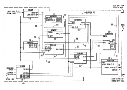
Figure 1 i8 a block diagram o~ a repeater node.
Figure 2 is a schematic diagr~m of a framer.
Figures 3R and 3B are schematic diagrams of storage cir-
cuitry. ~ ~
Figure 4 is a schematic diagram of an input pointer.
Figure 5 is a schematic dLagram of an output pointer.
Figure 6 is a schematic diagram of an input controller.
-
" :
-~6-
. ~ :
,
,
1322419
Figure 7 is a schematic diagram of a synchronizer.
Figure 8 is a schematic diagram of idle detection cir-
cuitry.
Figure 9 is a schematic diagram of an output idle counter.
Figure 10 is a schematic diagram of a reset state machine.
Figure 11 is a state diagram for a reset state machine.
Figure 12 is a schematic diagram of overflow/underrun
detection circuitry.
Figure 13 is a schematic diagram of clock generator cir-
cuitry.
Figure 14 is an error detection timing chart.
Figure 15 is a write pointer timing chart.
Figure 16 is a read pointer timing chart.
DESCRIPTION OF THE PREFERRED EMBODIMENTS
Reference will now be made in detail to the preferred
embodiments of the invention, example~ of which are illustrated
in the accompanying drawings.
A preferred embodiment of the repeater node is shown in
~ ~ Figure 1 and i~ represented~generally by the numeral 10. The
;~ 20 ~ repeater node i8 provided in a data communication system, which
includes a number of node~ coupled in a network~for transferring
frame~ of data from a sou~rce~node~to a destination node through
the repeater node. The repea~er node receives a~number of bits
of data in a frame from an~upstream node and transmits the num-
;25 ~ ber of b1ts~of data in the frame to~a downstream node. Eachnode in the network~transmits data in serial format in synchro-
nism with its own independent clock.
, ~ , . 1 ~. : . : ~
~ 17-
, ~. , , , ,, ~
: :
' :
.
- 1322419
In accordance with the invention, the repeater node in-
cludes a parallel asychronous elasticity buffer. The buffer is
represented generally by the numeral 12 in Figure 1.
Repeater node 10 may include means for providing a transmit
multibit clock signal that is in synchronism with the indepen-
dent clock of the upstream node, and means for providing a local
multibit clock signal that is in synchronism with the indepen-
dent clock of repeater node 10. In a preferred embodiment of
node 10, a transmit byte clock signal (TBYTECLK) corresponds to
the transmit multibit clock signal, and a local byte clock sig-
nal (LBYTECLK) corresponds to the local multibit clock signal.
Pxeferably, the transmit byte clock signal and local byte signal
are provided by clock generator circuitry 14, shown in Figure 1.
As shown in the embodiment of Figure 1, parallel
a~ynchronou~ elasticity buffer 12 is pr~vided with the transmit
byte clock signal and the local byte clock signal by clock gen-
erator circuitry 14. A local oscillator circuit (not shown) in
repeater node 10 generates a 12.5 megahertz TTL-compatible sig-
nal corresponding to a byte clock signal (BYTCLK) and a 25
megahertz TTL-compa~ible signal corresponding to a symbol clock
signal (5YNCLX) as input to clock generator circuitry 14. A
clock and data conversion chip (not shown) in repeater node 10
provides a 12.5 megahertz TTL-compatibl:e~signal corresponding to
a reaovered byte:clock~signal (R~CLK) as~ another input to clock
: 25 ; generator circuitry 14.
In a preferred embodiment, repeater node 10 is coupled to a .
: token rin~ network, such as a network in which data
,, ~ ,, ~
: -18-
.,, ~
:. , .: : - ':
': ' ' ' ~ .
- 1 322Dr t 9
communication is performed in accordance with the FDDI protocol.
As embodied herein, repeater node 10 receives and transmits data
in accordance with the FDDI protocol.
In the FDDI protocol, the period of the local byte clock
signal for each node is nominally equal to the period during
which ten individual bits of data (comprising one byte or two
symbols) are serially transferred between two nodes. The time
required for serial transfer of each individual bit of data is
referred to as a ~bit time." Therefore, in a preferred embodi-
ment of the invention, ~he transmit and local multibit clock
signals have perioda equal to ten bit times, and the symbol
clock signal has a period equal to five bit times.
In a preferred embodiment of the invention, data is written
into elasticity buffer 12 using the transmit byte clock signal
provided by clock generator circuitry 14, and data is read from
elasticity buffer 12 using the local byte clock signal provided
by clock generator circuitry 14. As embodied herein, the trans-
mit byte clock signal is used to drive a framer 16, a write
(input) controller 18, a write (input) pointer ~0, a temporary
address memory 22, and a number of multibit storage elements 24. ;
;! The local byte clock signal is used to drive a read (output)
I
controller 25, a read (outpu~) poin~er 28, a read (output~ i
- ~ buffer 30, and~a aynchronizer~32.~ ~ ~
In~accordance with the i~nventlon, the~elasticlty buffer in-
cludes réceiving mean3 ~or providing in parallel format, in re-
sponse to a transmi~ multibit clock ~ignal that is in ~ychronism
with an independent clock of the upstream node, a multibit data
:: ~
1 3224 1 9
unit having a fixed number of bits of data received from the up-
stream node. In a preferred embodiment, this means is provided
by ten buffer input data lines 34 (Figures 1 and 2) and may also
include framer 16.
Input data is clocked into framer 16 from the clock and
data conversion chip one symbol (five bits) at a time using both
the rising (TBYTFCLK H) and falling (TBYTECLK L) edges of the
transmi.t byte clock signal from clock generator circuitry 14.
Framer 16 accepts ~ive-bit wide parallel data from the clock and
data conversion chip (not shown). The clock and data conversion
chip in repeater node 10 receives input data from the upstream
node and provides TTL-compatible data to framer 16 synchronously
with the rising edge of the transmit byte clock signal. With
each rising edge of the transmit byte clock signal, one byte of
data is clocked out of framer 16 onto ten buffer input data
lines 34 for input to one multibit storage element 24.
Figure 2 shows the structure for framer 16 in repeater node
10, which is coupled to an FDDI network. Generally, incoming
da~a to elasticity buffer 12 is not framed into proper FDDI sym-
bols. For this reason, framer 16 is at the input stage of elas-
ticity buffer 12 to align input data to form proper symbols
before input data is tranferred through the elasticity buffer.
Th~ elasticity buffer of the present invention may include
means for detecting receipt by the repeater node of a first
multibit~data unit o a frame from the upstre~m node. Prefer-
ably, this detecting means is~ provided by comparP logic 36 in
framer 16. In the FDDI protocol, the first byte in a new frame
-20-
,
- .
1 )22~r 1 9
contains a starting delimiter consisting of the symbols J and K.
Compare logic 36 detects the presenc~ of the starting delimiter
at the beginning of each frame. Framer 16 uses the starting
delimiter to determine proper symbol boundaries for input data
received from the upstream node.
In addition to compare logic 36, framer 16 includes a sym-
bol (five bit) wide holding register 38, a 29-bit wide
three-part shift register 40, and a multiplexer 42. When a
first symbol of input data from the clock and data conversion
chip is clocked into framer 16, the first symbol is stored in
symbol-wide holding register 38 on the falling edge (TBYT~CLK L)
of the transmit byte clock signal. On the rising edge (TBYTECLK
H) of the transmit byte clock signal, a second symbol from the
clock and data conversion chip, toge~her with the first symbol
stored in holding register 38, are shifted into a first part 40A
of shift register 40, which i~ one byte (ten bits) wide. At the
same time, data previously stored in shift register part 40A is
shifted into a shift register part 40B, which is also one byte
wide, and the nine least significant bits of data previously
stored in shift register part 40B are shifted lnto a shift reg- j
ister part 40C, which is nine bits wide. Any data previously
; stored in shif~ register part 40C, as well as the most signifi-
, i
cant bit previously stored in shi~t register~part 40B, is dis-
carded on the rising adge of the transmit byte clock signal.
In the FDDI protocol, the starting delimiter field at thP
start of each frame consists of~the JX symbol pair, which corre-
sponds to the code group 1100010001. Compare logic 36 is
:~ :
- -21-
, .
13224t9
coupled to shift register parts 40A and 40B and checks for the
presence of this ten-bit starting delimiter code group. The
starting delimiter code group first appears in one of ten possi-
ble paths (i.e., shift register bits 0-9, 1-10, 2-11, ..., or
9-18). When compare logic 36 detects the presence of the
starting delimiter code group in one of these ten paths, a JK
detect signal is provided by compare logic 36 to write (input)
controller 18 on two lines.
In framer 16, after detection of a starting delimiter, the
appropriate path within the framer is selected so that the input
data received from the upstream node can correctly be provided
as buffer input data to one storage element 24. On the next
rising edge of the transmit byte clock signal, an output path is
selected that corresponds to the particular bits in shift regis- ;
ter 40 in which the starting delimiter was detected. Multi-
plexer 42 establishes the appropriate ou~put path by selecting a
group of ten consecutive bits in shift register parts 40B and
40C for output on ten buffer input data lines 34. Once an out-
put path is selected by multiplexer 42, it remains selected
until a starting delimiter i5 detected in one of the other nine
group~ of shift register bits.
In accordance with the invention, elasticlty buffer 12 has
storage means including a fixed number o multibit storage ele-
men~s, coupled to the receivin~ means, for sto~ing the multibit
data unit in parallel format in one of the storage elements,
.
wherein each storage element has a unique address. As embodied
herein, the storage means is proyided by at least four and
.
-22-
.
132241q
preferably eight multibit storage elements 24, each of which
store~ one byte (ten bits) of data.
As shown in Figures 3A and 3B, in a preferred embodiment of
the storage means one byte of buffer output data is provided on
S ten buffer output data lines 44A-44J for subsequent transmissionto a downstream node. The storage means receives as inputs the
transmit byte clock signal, one byte of buffer input data re-
ceived from the upstream node on buffer input data lines 34, a
write address on eight (decoded) write address selection lines
46, and a read address on three (encoded) read addre~s selection
lines 48.
A preferred structure for one of the eight storage elemants
24 is shown in Figure 3A. Storage element 24 includes ten
flip-flops 50A-50J, each flip-flop storing one of the ten bits
' in a byte of data. When the unique address corresponding to 'I
this storage element is selected as a write address, a signal is i
provided on decoded write address selection line 46 coupled to
that storage element, and no signals are provided on the other
seven decoded write address selection line~. The provlding of a
signal on this write address selection line causeo enable logic
, 52 to couple each buffer input data line 34 to~a corresponding
flip-flop 50. ~ a result, a byte of input data is written into
storage element 24 when the flip-flops are clocked by the trans-
m1t byte clock signal.
Preferably, ten multiplexers 54 are providedl as shown in
Figure 3B, to select one of;eight~storage elements 24 for cou-
pling to buffer output~data lines 44. One multiplexer 54 is
-23-
- 1 3224 1 ~
coupled to each buffer output data line 44 ana G~r~spands to a
single bit in the multibit data unit. Each multiplexer 54 re-
ceives one bit from each one of the eight storage elements 24.
In a preferred embodîment, three encoded read address selection
lines 48 are used to designate the read address and are also
input to multiplexers 54. The read address corresponds to the
unique address of one selected storage element 24, and multi-
plexers 54 respond by coupling flip~flops 50 of the selected
storage element 24 to buffer output data lines 44.
In accordance with the invention, parallel asynchronous
elasticity buffer 12 includes transmitting means, coupled to the
storage means, for providing in parallel format, in response to
a local multibit clock signal that is in synchronism with the
independent clock of the repeater node, one of the multibit data
units stored in the storage means. Preferably, the transmitting
means is provided by ten buffer output data lines 44 shown in
Figure 1, and may also include read ~output) controller 26 and
read (output) buffer 30.
In a preferred embodiment, repeater node 10 may include
read (output) buffer 30. As shown in Figure 1, buffer 30 re-
ceives ten bits of output data over lines 55 from read con-
troller 25. Read controller 26 receives one byte of data from
the storage mean on ten buffer output data lines 44. The read
i
controller i provided between the storage means and buffer 30
to add additional idle bytes to the preamble under certain cir-
.
` cumstance~ in order to expand the gap between two frames. Out-
put logic (not shown) in controller 26 either provides the
..
; -24-
: ~ .
,
- t 3224 1 9
buffer output data from the storage means to buffer 30, or else
responds to a force signal by providing an idle line-state byte
to buffer 30.
On each falling edge of the local byte clock signal, the
output data from read controller 26 is loaded into an input
stage of buffer 30. On the rising edge of the byte clock signal
(BYTCLK H), output data in the input stage of buffer 30 is then
clocked into an output stage of buffer 30. In this way, output
data is retimed from the local byte clock signal provided by
clock generator circuitry 14 to the byte clock signal provided
by the local ocillator in node 10. On the rising edge of the
byte clock signal, the five most significant bits in one byte
(i.e., the high order symbol) are provided from the output stage
of buffer 30 on five output lines 56 for one symbol time. On
the falling edge of the byte clock signal, the five least sig-
nificant bits ln the byte (i.e., the low order symbol) are pro-
vided from the output stage of buffer 30 on output lines 56 for
one symbol time.
In accordance with the invention, there is provided write
pointer means, coupled to the storage means, for selecting as a
writ~ address the address of a~storage element to store the next
multibit data unit providèd by the receiving means. As embodied
herein, the write pointer means may correspond to write (input)
!
pointPr 20.
In a preferred embodiment, write (input) pointer 20 is a
counter clocked by the transmit byt clock ignal. Write point-
er 20 generate3 a write address corresponding to the address of
,
, ' ' . ' '
.
, . .
1 322~ 1 9
one selected storage element 24 by incrementing the input point-
er count in response to tne transmit byte clock signal. Pointer
20 provides the write address to each of eight storage elements
24 on eight decoded write address selection lines 46, and also
provides the write address to temporary memory 22 and synchro-
nizer 32 on three encoded write address selection lines 58A-58C.
A preferred structure for write pointer 20 is shown in Fig-
ure 4. ~rite pointer 20 is a free running 3-bit counter having
eight possible states. Each state corresponds to a unique
address designating a single storage element 24 to store the
buffer input data on lines 34. Flip-flops 60A-60C provide a
three-bit input pointer count (IP) as the write address on three
encoded write address selection lines 58A-58C. The outputs from
flip-flops 60 are also supplied as inputs to decoder logic 62,
which decodes the three-bit write address and provides a signal
on only one of the eight decoded write address selection lines
46A-46H.
A~ embodied herein and as shown in Figure 4, write pointer
20 is a gray code counter. Counter logic 64 generates the next
write address for input to flip-flops 60 by uslng the input
pointer count (IP~ curren ly output hy flip-flops 60. Counter
, logic 64 changes the s~ate of one and only one bit of the input
pointer count ~IP). The CouDt proceeds ln a sequence such as
.
~ the following: 000, OOlr 011, 010, 110, 111, 101, 100, and then
~r
returns to 000.
The invention include~ read pointer means, coupled to the
storage means, for selecting as a read address the address of a
-26-
:
''' ' ., ','',' ,.. :' - '' " :
- : .. .
.
, ' ' ' ' ' . ' . '
' ~ ' ' ' .
1 3224 1 ~
storage element to provide the next multibit data unit output by
the ~ransmitting means, wherein each multibit data unit is out-
put in first-in, first-out order. Preferably, the read pointer
means is provided by read (outputj pointer 28.
In a preferred embodiment shown in Figure 5, read (output)
pointer 28 is a loadable counter clocked by local byte clock
signal LBYTECLIC. Read pointer 28 increment~ the output pointer
count (OP) in response to local byte clock signal LBYTECLK, and
selects a single one of eight storage elements 24 to provide the
next byte of buffer output data on buffer output data lines 44.
Flip-flops 66A-66C provide a three-bit output pointer count (OP)
as the read address on three encoded read address selection
lines 48A-48C to multiplexers 54, which select the bits stored
in o~e of the eight storage element~ for output. The read
address on encoded read address oelection lines 48 is also pro-
vided to synchronizer 32.
As embodied herein, read pointer 28 is a gray code counter.
Counter logic 68 generates the next read address for input to
three~flip-flops 66 u ing the output pointer count (OP) cur~
rently output by flip-flops 66. Counter logic 68 changes the
! stata of one and only one bit of the output pointer count (OP).
In the pre~ent invention, in1t1a1ization~means 15 provlded
for initializing the elasticity~uffer to prevent~simultaneous
~; se1ection of~the ~same addreso as a read~address and a write
25~ ~ addre~ , wherein in~response~to initia1izat1on, a write address
is selected as a~read~addres;s after a predetermined delay. In a
preferred embodiment, ~he initialization means ma~ include
~ -27-
.. ~ . . . ... - . .
.: . . :
.
. ~ .
' ' ' :
. ~ ' .' ' , .
.
.
1 ~ J ~ 4 1 9
synchronizer 32, write (input) controller 18, and read (output~
controller 26.
A preferred embodiment of write (input) controller 18 is
shown in Figure 6. Controller 1~ receives the JK detect signal
provided by compare logic 36 in framer 16, the buffer input data
provLded on ten buffer lnput data lines 34 by multiplexer 42 in
framer 16, and the transmit byte clock signal TBYTECLK provided
by clock generator circuitry 14. A function of write (input)
controller 18 is to detect the presence of two conditions which
result in resetting of elasticity buffer 12. Controller 18 gen-
erates an enable signal which is provided to synchronizer 32 on
line 71 and a pre-enable signal which is provided to temporary
addresq memory 22 on line 69.
As shown in Figure 6, write controller 18 includes input
error overlook circuitry 70. Error overlook circuitry 70 is a
state machine that functions as an error filter. Circuitry 70
monitors the data on ten buffer input data lines 34 and is re-
sponsive to the transmit byte clock signal TBYTECLK. In a pre-
ferred embodiment for use in FDDI ne~works, repeater node 10 re-
ceive~ from the upstream node a preamble including a number of
idle line-state bytes, which occurs prior to transmission of the
starting d~limiter for the next frame of data. After one idle
line-state byte is detected, circuitry 70 provides an input idle
counter enabIe signal IICE. Circuitry 70 continues to provide
the input idle counter enable signal until at least two consecu-
~ tive bytes are detected that do not corre~pond to idle
: ~ line-state bytes. Circuitry 70 thereby prevents a single byte
-28-
'
- 1 3224 1 q
error during transmission or detection of a string of idle
line-state bytes from interfering with reset of the buffer.
Preferably, controller 18 includes an input idle counter
72. Cowlter 72 is enabled by the input idle counter enable sig-
nal IICE, and is r~set when the enable signal from circuitry 70
is not provided. Counter 72 is a four-bit counter clocked by
the transmit byte clock signal TBYTECLK that keeps track of the
number of idle line-state bytes received by repeater node 10
from the upstream node. Counter 72 provides an input idle count
flag sixteen signal IICF16 whenever sixteen consecutive idle
line~state bytes have been provided on buffer input data lines
34 by framer 16. Sixteen idle line-state bytes have passed
through framer 16 when counker 72 reaches a count of fifteen.
In a preferred embodiment of repeater node lO, elasticity
buffer 12 is initialized (reset) whenever controller 18 detects
one of two possible reset conditions: (1) receipt of sixteen
con~ecutive idle line-state bytes from the upstream node; or (2)
receLpt of the first byte of data in a frame from the upstream
node. As shown in Figure 6, the JK detect signal (on two lines)
from framer 16 and the IICF16 signal are pro~ided to three AND
gate~ 74. AND gates 74 in combination wi~h an OR gate 76 indi-
cate that controller 18 has de~ected the presence of a re~et
condition.
As shown in Figure 6, an~input wait timer 78 Ls preferably
incIuded in write controller 18. Input wa~it timer 78 is a
12-state counter which incrementu when clocked by the transmit
~ ~ byte clock signal TBYT2CLK until it returns to its initial
::
29-
`,',',' ' - ~ .
. ~ ,' ' '
' '
1 3~24 1 '~
state. A timer signal is provided by timer 78 whenever it is in
this initial state. Input wait timer 78 leaves the initial
sta~e when write controller 18 provides a pre-enable signal on
line 69 in response to detection of either of the two reset con-
ditions. Therefore, after the pre-enable signal and the enable
signal are provided by write controllar 18 in response to detec-
tion of a reset condition, timer 78 provides a waiting period of
twelve byte times before it returns to the initial state. The
timer fiignal is not provided during this waiting period to
ensure that adequate time exists for completion of a previous
initialization of elasticity buffer 12. The timer signal is
provided to AND gates 74, which permits controller 18 to provide
the pre-enable and enable signals if a reset condition is
detected, unless initialization of buffer 12 commenced within
the waiting period provided by timer 78.
In a preferred embodiment of write controller 18, three
flip-flops 80A-80C are provided that are coupled to an OR gate
82, which provides the enable signal. These flip-flops are re-
sponsive to either the rising (TBYTECLK H) or falling (TBYTECLK
L) edge of the transmit byte clock s~gnal. Thls circultry
enRur~s that write controller 18 provides the enabl~ signal for
two full cycles of the transmit byte clock signal TBYTEChK. On
the falling edge of trans~it clock byte signal TBYTECLX immedi-
; a~ely fol~lowing the detection of a reset condition, the enable
25 ~ signal will be provided if input wait timer 78 is in its initial
; state. The enable signal is provided for two byte times, i.e.,
until the falling edge of the third transmit ~yte clock signal
, ~ "
following detection of a reset conditions.
30-
,.~.,- - ' , . ' ' ' .
1 3224 1 9
In a preferred embodiment of the invention, elastici~y
buffer 12 includes memory means for storing at least one ini-
tialization address. The memory means, in response to detection
of the first multibit data unit of a frame, stores from the
write pointer means as the initialization address for the read
pointer means the write address corresponding to the storage
element selected to store the first multibit data unit.
As shown in Figure 1, the memory means may be provided by
temporary address memory 22. Temporary address memory 22 re-
ceives as inputs the pre-enable signal on line 69 from write
controller 18, the input pointer count (IP) on lines 58 from
write pointer 20, and the transmit byte clock signal TBYTECLK.
Temporary address memory 22 preferably contains flip-flops for
storing as the initialization address for read pointer 28 the
input pointer count corresponding to the storage element which
iR selected to store the first byte (i.e., the starting
delimiter) in a frame. The initialization address is provided
on three lines by temporary address memory 22 to read pointer 28
and is designated as the address-in-memory (AIM) signal. On the
rising ed~e of the transmit byte clock signal following provid-
ing of the pre-enable signal by write controller 18, the input
pointer count is incremented by write pointer 20, and this write
addre~s ig loaded into temporary addres~ memory 22.
The preferred asynchronous elastic1ty buffer is synchro-
nized only once during transmission of each frame of data. In
synchronous elasticity~buffers, each data unit written into the
buffer is pre-synchronized, increasing the probability of errors
31-
,
.
132241q
due to metastability. In contrast, in the preferred embodiment
of the invention, the read and write operations are asynchronous
(write operations are in synchronism with the kransmit clock
byte signal and read operations are in synchronism with the
local clock byte signal).
In a preferred embodiment of the invention, synchronizer 32
is provided to synchronize the writing and reading of the stor-
age means once per frame of data. Preferably, synchronization,
as well as initialization, occurs in response to receipt of the
first byte in a new frame. However, other embodiments of an
asynchronou6 elasticity buffer can be constructed with equiva-
lent circuitry in which synchronization and/or initialization of
the elasticity buffer occurs at another time among various times
before, after, or during transmission of each frame.
A preferred embodiment of synchronizer 32 is shown in Fig-
ure 7. 5ynchronizer 32 receive~ the enable signal on line 71
from write controller 18 and provides an output controller
enable flag signal OCEF to read controller 26 on line 83. The
enable signal 1~ provided by write controller 18 for two full
cycleY of transmit byte clock signal TBYTECLK, and is provided
beginning on the falling edge of transmit byte~clock signal
TBYTBCLK following detection of a reset condition. In synchro-
nizer 32, the enable signal is sampled by a dual rank synchro-
nizer including three flip-flops 84A-84C on the falling edge of
the local byte clock signal. The output controller enable flag
signal OCEF is provided if the enable signal is present when
sampled by the falling edge of local byte clock signal LBYTECLK,
.: , -~ i
-32-
1 32~ 1 9
except synchronizer 32 does not provide output controller enable
flag signal OCEF to read controller 26 for more than two local
byte clock signal periods.
As shown in the Figure l embodiment, the elasticity buffer
includes read (output) controller 26. Read controller 26 re-
ceives as inputs one byte of buffer output data on lines 44,
local byte clock signal LBYTECLK, output controller enable flag
signal OCEF from synchronizer 32, and an equal signal from read
pointer 28. In response to these inputs, read controller 26
provides one byte of output data to read (output) buffer 30 on
lines 55, and provides a read pointer load enable signal LOAD to
read pointer 28 on line 85.
As embodied herein and shown in Figure 8, read controller
26 includes idle detection circuitry 86. Circuitry 86 receives
a byte of buffer output data from one storage element 24 via
lines 44. For an FDDI network, the 5-bit code group correspond-
ing to an idle symbol corresponds to lllll. Therefore, an idle
byte i~ detected by inputting the buffer output data to AND
gates 88A-88B. In a preferred embod1ment, read controller 26
can force an idle byte to be substituted for the actual buffer
:
: ~ ~ output d~ta on lines 44 by providing a force signal. The force
signal i~ also monitored by idle detection cixcuitry 86. The
~ ~: force slgnal is input to an OR gate 90 along with the output
: : from an AND gate B8C. OR~gate 90 provides an idle byte detec-
tion signal on line 9l whenever an~idle byte is being ~rans-
mitted from read controller 26 to read bufer 30 and the down-
stream node.
-33~ :
.
,
~,,
. ,.
: ' ,
- 1 3224 1 9
Preferably, read controller 26 includes an output idle
counter 92, as shown in Figure 9. Output idle counter 92 is an
eight state counter which keeps track of the number of succes-
sive idle bytes provided to read buffer 30. Whenever idle
detection circuitry 86 detects idle bytes on buffer output data
lines 44 or the presence of the force signal, the idle byte
detect'on ~ignal on line 91 is input to AND gates 94A-94C. As
long as idle bytes are being transmitted to the downstream node,
AND gates 94A-94C provide outputs to three flip-flops 96A-96C
that enable incrementing of counter 92 on the following falling
edge of local byte clock signal LBYTECLK. ~han counter 92
reaches the final state, it remains in that state, indicating
that at least eight idle bytes have been transmitted to the
downstream node. Output idle counter 92 is reset only when idle
detection circuitry 86 indicates that idle bytes are no longer
being transmitted to the downstream node. Each flip-flop 96
provides one bit in the three-bit output idle count, which is
referred to a~ output idle count signal OIC.
In the preferred embodiment, the output idle count signal
is utilized by read controller 26 in determlning the number of
idla bytes that are being transmitted to the downstream node.
A~ shown in Figure 9, an output idle coun~ flag eight signal
OICF8 is provided by logio 98 in read controller 26 whenever the
output idle count signal indicates that eight or more idle bytes
are being transmitted to the~downstream node. Similarly, logic
100 in read controller 26 asserts an output idle count flag
seven ~ignal OICF7 whenever counter 92 indicates seven or more
idle byte~ are being transmitted to the downstream node.
3~-
- 1 3224 1 q
As embodied herein, the read controller performs a process
that requires the storage means in elasticity buffer 12 to be
progressively more full when initialization occurs before
deleting idle bytes from the preamble preceding a subsequent
frame. For a repeater node connected to an FDDI network, the
minimum number of idle bytes between frames is six and the ini-
tial number of idle bytes provided between frames by a source
node is eight.
In order to implement the preferred process, elasticity
buffer 12 includes additional storage elements 24 so that read
controller 26 can wait an additional time period before having
to add or delete one or more idle bytes from the preamble. As
embodied herein, implementation of the process requires the use
o a total of eight storage elements 24, wherein four of these
elements are additional storage elements provided to increase
the range of buffer 12 by forty bits (four bytes).
In selecting a proce~s for avoiding unnecessary shrinkage
of the interframe gap, a trade off is made between lowering the
probability of deletion of idle bytes resulting in the pre~mble
having fewer than a mlnimum n~mber of idle bytes, and increasing
the number of storage elements 24 and the amount of delay in
transmission. In the preferred embodiment, a method and appara-
tu~ i8 provided that uses multiple thresholds in order to
achieve the best results when these factors are considered.
25 ~ Table I il1ustrates the use of~multiple thresholds in an
ela ticity buffer. However,~the buffer delays in Table I are
for a buffer that does no~ include any~circuitry for error
, ~
~,
~ -35-
~:
. ., ,, ~-
" , ,. ~ ~ -
1 3224 1 9
detection. When additional hardware included in a preferred
embodiment of the invention to detect impending error conditions
is considered, the buffer delay increases by ten additional bits
for reasons that will be explained later.
TABLE I
Number of Elasticity Buffer
Idle Bytes Delav in Bits
greater than 8 5-lS
8 5-25
7 15-45
6 35-55
less than 6 45-55
The decision of whether to add ox delete an idle byte from the
preamble is a function of the number of idle bytes being trans-
mitted to the downstream node as well as tha fullness of the
elasticity buffer. The fewer the number of idle bytes being
transmitted, the closer to overflow elasticity buffer 12 must be
before another idle byte will be deleted. Using this process,
elasticity buffer 12 is four bytes larger than would otherwise
20 ~ be necessary, the maximum node delay is increased by 320
nanoseconds (four bytes), and the avérage node delay is in-
crea~ed by forty nanoseconds (five bitSj. If the process illus-
trated above is not utilized,~ the elasticity buffer delay will
; be at least 5-lS bits regardless of the number of idle hytes in
the preamble being transmltted. ~In contrast, the illustrated
proces increase the size of th~ initial ~elay as ~hP gap
between frames becomes smaller.
.. ...
-36-
.
- 1 3224 1 9
Preferably, read controller 26 includes a reset state ma-
chine 102, which is shown in Figure 10. Additionally, the pro-
cess implemented by reset state machine 102 is illustrated by a
state diagram in Figure 11.
In accordance with the invention, the write pointer means
and/or the read pointer means may select an initialization
address stored in the memory means in response to a control sig-
nal from the initialization means. Preferably, reset state ma-
chine 102 is a six-state sequential machine which utilizes the
number of idle bytes counted by output idle counter 92 to deter-
mine when to provide a read pointer load enable (load) signal on
line 85, which corresponds to the control signal. The read
pointer load enable signal provided by reset state machine 102
to read pointer 28 causes the read pointer to be loaded with the
stored initialization address (AIM) provided by temporary
address memory 22, as shown in Figure 5. Initialization tre-
setting) of read pointer 28 causes selection o~ the storage ele-
ment containing the starting delimiter for the subsequent frame.
In response to initialization, the write address selected by
write polnter 20 is selected as a read address by read pointer
28 after a predetermined delayO Providing of the load signal by
resat state machine 102~thereby enables ~ransmission of the
starting~delimiter to the downstream~node. ~
As;shown in Figure 10, reset state machine 102 includes
three fl~p-f1Ops 104A~104C that provide the three~bit reset
state signal RS that indicates the;current state. The reset
sta~te signal RS is provlded to an~AND gate 106 which asserts the
! ` :: .~ :, ~, '
-37-
~: :
.
: ... . . ~
,
- ~ ' . . '
. .
.
1 3224 1 9
read pointer load enable signal when reset state machine 102 is
in state 100. The inputs to flip-flops 104 are provided by
logic 108, which is responsive to the output controller enable
flag signal provided from synchronizer 32 on line 83, and to
output idle count and output idle count flag signals provided by
output idle counter 92.
As shown in Figure 11, reset state machine 102 usually
loops in idle state 000 until the output controller enable flag
signal OCEF is provided. In response to the providing of OCEF,
the output idle count signal OIC is sampled on the next rising
edge of the local byte clock signal.
~hen the OCEF signal is provided and the output idle count
flag eiqht signal OICF8 has been set, state machine 102 proceeds
to state 100. The O~CF8 signal indicates that eight or more
idle bytes are being transmitted to a downstream node.
. (Although only seven or more idle byte~ have actually been
detected at this time, an additional idle byte will be trans- -
mitted before reset state machine 102 can return to idle state
000.) During the reset state 100, the load signal is output to
. read pointer 28 on line 85. Read pointer 28 is driven by the
, falling edge of local byte clock signal LBYTECLK and will there-
: fore ~elect the address of the storage~element.containing the
. starting delimiter for ~he subsequent frame on the falling edge
of the local:byte clock signal following entry of reset state
: :: ~ , : :
machine 102 into reset state 100. The count of eight idle bytes
i5 more than a high threshold number of idle bytes, which is
preferably set to equal seven bytes. Therefore, as shown in
-38-
,,
- ~ 3224 1 9
Table I, the delay immediately after initialization in selecting
the wxite address as the read address is always at least f ive
bit times, but transmlssion of the starting delimiter for the
subsequent frame may be further delayed by read controller 26.
When eight or more idle bytes are not being transmitted to
khe downstream node, reset state machine 102 proceeds from state
000 to state 001 in response to the OCEF signal indicating re-
ceipt of the starting delimiter for the subsequent frame. Reset
state machine 102 remains in state 001 for one byte time and
monitors whether the output idle count flag seven signal OICF7
is provided indicating that seven idle byteR are being trans-
mitted to the downstream node.
If seven idle bytes are being transmitted to the downstream
node, state machine 102 proceeds from state 001 to reset state
' 100, and th~n performs in the manner previou~ly described. ~hen
the high threshold number of seven idle bytes is being trans-
mitted to the downstream node, the load signal i~ not provided
by read controller 26, thereby delaying transmission of the
starting delimi~er to the downstream node e~en though the write
1 addres~ has been selected as the read address. Since reset
state machine 102 has to proceed to state 001 beforQ it enters
j the re e~ stata l00, transmission of the starting delimiter is
:
~I delayed for one additional byte time compared with a situation
;~ ~ in whlch eight or more idle hytes are~being transmi~ted. Thus,
as shown in Table I, the minimum elasticity buffer delay is 15
bit times when seven idle by~es are being transmitted.
-39-
:~ - , ~ ;
' ::
'', '
-'
,
1 3224 1 9
If fewer than seven idle bytes are counted by output idle
counter 92, reset state machine 102 proceeds from state 001 to
state 011, where it remains for one byte time. If fewer than
seven idle bytes are counted by output idle countex 92, reset
state machine 102 then proceeds to state 111, where it remains
for an additional byte time. When the output idle count signal
indicates that six idle bytes, which preferably corresponds to a
low threshold number, are being transmitted to the downstream
node, then reset state machLne 102 can proceed from state 111 to
re~et state 100. Thus, in response to an idle byte count
indicating that a low threshold number of six idle bytes is
being transmitted to the downstream node, reset state machine
102 does not provide the load signal, thereby delaying transmis-
sion of the starting delimiter to the downstream node for an
even longer time period. Reset state machine 102 is required to
enter two additional states before it enters re~et state 100 and
asserts the control signal. This corresponds to the process
shown in Table I, in which an idle byte count of six results in
a minimum delay that is two byte time~ longer than the minimum
i delay when seven idle bytes are being tran~mitted to the down-
stream node.
At times when output idle counter 92 indicates that fewer
than six idle bytes are being transmitted to the downstream
node, s~ate machine 102 proceeds from state 111 to state 110,
25~ where it remains for one byte time. As long as two or more idle
bytes are being t.ran~mitted ~o the downstream node, or if the
read address (OP) equals the stored initlalization address
.
,
1 3224 1 9
(AIM), reset state machine 102 will then proceed to reset state
100. In this situation, reset state machine 102 enters four
additional states before proceeding from idle state 000 to reset
state 100. Thus, when a lower threshold number of idle bytes
equal to five or less is being transmitted to the downstream
node, transmission of the starting delimiter is delayed for an
additional byte time. As shown in Table I, the minimum elastic-
ity buffer delay is 45 bits whenever fewer than six idle bytes
are being transmitted to the downstream node.
In unusual situations, reset state machine 102 may leave
state 110 and proceed to initial state 000 without detection of
a single idle byte. This may occur if the write and read point-
ers have drifted far from their initial spacing. In this situa-
tion, data may be deleted by repeater node 10 if reset state ma-
chine 102 enters the reset state 100. Therefore, if one idle
byte has not been detected, and if the read address (OP) does
not equal the stored initialization address, state machine 102
proceeds directly from state 110 to the initial state 000, and
~ no initialization (reset) of elasticity buffer 12 occurs.
As embodied herein~ read pointer 28 provides an equal sig-
nal to read controller 26 to indicate that elasticity buffer 12
is ready to begin transmitting the first byte of the subsequent
frame to the downstream node. The equal signal is provided by
; read pointer 28 when the output pointer count (OP) matches the
stored initialization address (AIM). This occurs only when the
s~orage ele~ent 24 selected by read pointer 28 to provide buffer
output data to bufer 30 (via read controller 26) contains the
first byte (the starting delimiter~ in the subsequent rame.
-4I-
' '
: ' .
,
1 3224 1 9
Preferably, read controller 26 includes a force idle state
machine 110, as shown in Figure 1. State machine 110 functions
to cause additional idle bytes to be transmitted to the down-
stream node whenever the load signal is not being provided, even
though the equal signal provided by read pointer 28 indicates
that buffer 12 is otherwise ready to begin transmitting the
fLrst byte (the starting delimiter) of the subsequent frame.
Force idle state machine 110 works in conjunction with reset
state machine 102 in order to add idle bytes to the preamble
between frames whenever transmission of the first byte in a sub-
sequent frame is delayed because the output idle count signal
from output idle counter 92 indicates the number of idle bytes
being transmitted to a down~tream node is at or below a certain
threshold.
~ In the preferred embodiment of the invention, the elastic-
ity buffer is initialized by providing a loadable read pointer
28 and free-running write pointer 20, and loading a write
address selected by write pointer 20 into read pointer 28 as a
read addra~s after a predetermined delay. However, an elastic-
ity buffer in accordance with the present invention can be pro-
, vided using oth:er equivalent~circuits. For example, the write
polnter means may correspond to a loadable counter, while the
i read pointer means corresponds to a~free-running counter. In
' such~an embodiment, initial~ization can be performed by loading
2s the write pointer mean~ with an Lnitial wrlte address~that will
be selected by the free-running read pointer means after a pre-
determined delay. In another embodiment, both the read pointer
42-
1 ~22~ 1 9
means and the write pointer means may be loadabls. In this
embodiment, initialization may be performed by loading different
addresses into the read pointer means and the write pointer
means. The initial read address for the read pointer means is
selected so that a predetermined delay will occur before the
read pointer means selects as the read address the initial write
address whlch was loaded into the write poLnter means. Other
possible embodiments of the invention may include one or more
state machines for selecting the read and/or write addresses
such that a predetermined delay elapses before a particular
write address is selected as a read address.
In accordance with the invention, the elasticity buffer in-
cludes detection means for detecting whether an error condition
corresponding to a write o~erflow or read underrun of a storage
element is impending by determing whether the same address is
selected as the write address and the read address during an
overlap time period ha~ing a duration equal to a threshold time
period. As embodied hereln and shown in Figure 12, the detec-
tion means may be provided by overflow/underrun detection cir-
c~itry 112.
Immediate and reliable detection of an overflow and~or
under-run condition is extrqmely difficult to perform if data is
asynchronously entering and leaving an elasticity buffer. How-
ever, by monitoring the read and write addresses for the elas-
ticity buffer, it is possible to detect when an over-
-~ ~- flow/under-run condition is impending. For example, if each
storage element in ths ela~ticity buffer contains ten bits (one
: ~ '
-43-
''
1 3224 1 9
byte in the FDDI protocol), then the elasticity buffer is on the
verge of overflow or underrun of a storage element when both the
read pointer and write pointer select the same address for ten
bit times (relative to either the local or transmit byte clock
signal).
An overflow or underrun of a storage element occurs when
that storage element is being written to and read from at the
same time. Furthermore, because of ~he finite propagation
delay~ and set-up and hold times associated with the logic in an
elasticity buffer, it is impossible for data to remain
uncorrupted if a single storage element i5 being written to and
read from at precisely the same time. Therefore, data corrup-
tion occurs before actual overflow or underrun of a storage ele-
ment if data is read from that storage element too soon after
being wxitten. Thus, it is important for a detection means to
indicate that an overflow or an underrun condition is impending
before an overflow/underrun occurs, thereby preven~ing corrupted
data from being transmitted through the elasticity buffer with-
out being flagged.
. As an example, the time when the detection means must
detect tAat a write overflow or read underrun of a storage ele- ;
ment i impending can be calculated. It:is;assumed that a par-
allel asynchxonous elasticity buffer:is provided in which each
:
storage element contains ten bits~(one~byte) of data, and in
25 ~ which ~alid data is obtaLned only lf ~ata i9 read from a storage
element at least four bit times~after it is written. In this
example, in order to guarantee that no~corxupted data will pass
-44-
: : -
1 3~4 1 9
through the elasticity buffer without being flagged, the detec-
tion means must detect that a write overflow or read underrun is
impending whenever the read pointer and write pointer select the
same address for an overlap time period of six bit times or
less.
Asynchronous operation of the read and write pointers makes
determination of the exact amount of any overlap in the two
pointers a non-trivial task. However, it is not as difficult to
determine when the two pointers overlap (i.e., select the same
address as the write address and the read address) during an
overlap time period falling within a given range. Furthermore,
if the independent clocks in the upstream node and the repeater
noda can be assumed not to differ in frequency by a large amount
(i.e., 50~ for the following example~)t then only one indepen-
dent clock need be used in sampling the read and right pointers
to determine the amount of poin~er overlap. If this assumption
is not valid, the same basic detection approach can be used,
although the detection means becomes more complicated because
both the transmit byte clock signal and the local byte clock
signal must be sampled in order to determine the amount of
pointer overlap.
The use of asynchronous read and write pointers in the
elasticity buffer makes it necessary to utilize gray code
counters for the pointers. Pointer overlap is detected by sam-
pling of the output~and input pointer counts. However, if one
of the two pointers increment~ its count immediately before sam-
pling, an uncertainty exists concerning the state of any bits
,:
i ~,
-45-
.
~ .
~ ' . . '; .
.
.~ , .
.
- 1 3224 1 9
that were changed. For example, if a count changes from 111 to
000, there is a possibility of glitching of the output because
it is possible to interpret the count as having any of eight
possible values. However, gray code counters provide counts
that change only one bit at a time and which can only be inter-
preted as one of two consecutive counts, thereby preventing
gliching of the output and reducing the probability of false
error detection.
In a preferred embodiment of the invention, the elasticity
buffer includes means for providing one or more sampling clock
signals. In this preferred embodiment, the detection means also
includes comparator means for comparing, in response to the sam-
pling clock signal, the write address and the read address.
Preferably, the sampling clock signal or signals are in synchro-
nism (L.e., maintain a fixed phase relationship) with the local
byte clock signal, as opposed to the transmit byte clock signal.
As embodied herein, and as shown in Figure 12, overflow/underrun
detection circuitry 112 use~ a first sampling clock signal pro-
vided by the sampling clock signal providing means to detect
whether a write overflow is impending, and uses a second sam-
pling clock signal out of phase with~t~he first sampling clock
signal to detect whether a read underrun is impending. Prefer-
ably, the first ~ampling clock signal is approximately 270 out
; of phase wlth the local byte~clock sLgnal, and the second sam-
~zs pling clock signal is approximately 180 out of phase with the
local byte clock signal.
: , ..
,
-46-
' ~
- 1322419
A preferred embodiment of a sampling clock signal providing
means for providing a first samp;ing clock signal to detect
whether a write overflow is impending and a second sampling
clock signal out of phase with the first sampling clock signal
to detect whether a read underrun is impending is shown in Fig-
ure 13. In this embodiment, clock generator circuitry 14 re-
ceives as i.nputs from a local oscillator the byte clock signal
and a symbol clock signal.
Clock generator circuitry 14 generates a local byte clock
signal LBYTECLK L, which will be referred to as the phase zero
local byte clock signal, and also generates a phase 180 local
byte clock signal LBYTECLK H and a phase 270 local byte clock
signal LBCLK270 H. Each of these outputs represents a different
phase of the independent clock in the repeater node. The symbol
' clock signal from the local oscillator is required because a
signal running at twice the frequency of the byte clock is
needed to easily obtain four different phases of the local byte
clock signal. If only two phases of the local byte clock signal
, were required, i.e., the phase zero byte clock signal and phase
180 local byte clock signal, then ~he neceiqsary sampling clock
signa1s can be easily provided using only an inverter. As 'i
embodied in Figure 13, the clock generator circuitry includes a
¦ flip-flop 114 that provides the phase 270 local byte clock sig-
nal, and a flip-flop 116 that provides both the phase zero local
i byte clock signal and the phase 180 local byte clock signal.
A first ca~e of interest occurs when the local byte clock
signal is faster than the ~ransmit byte clock signal. In this
: -
-47-
. . . ' ~
.. ~ , , .
. - .
.-, . . : ' .. .. . . :
. .
'' . ,'
'' ... ' , " '. ' .
- 1 3224 1 9
case~ the read address selected by the read pointer means
catches up with the write address selected by the write pointer
means. If the read and write pointers are compared, and there
is an overlap detected using a comparator means that samples
with the phase 180 local byte clock signal, there is an overlap
time period having a duration equal to five bit times minus the
propagation delay through any comparator logic and the set-up
times of any flip-flops in the read and write pointers. Depend-
ing on the circuit design and device technology used, these
propagation delays and set-up times may have a duration of less
than a single bit time. Therefore, under these circumstances, a
detection means using the phase 180 local byte clock signal can
determine that the same address is selected as he write address
; and the read address during an overlap time period having a
1 duration of between four and five bit times. If the propagation
delays and set-up times are as high as three bit times, then the
overlap time period that can be determined has a duration of
between two and five bit times.
A second case of interest occurs when the transmi~ byte
, clock signal i8 faster than the local~byte clock signal. In
. this case, the write address selected by the wri~e pointer means
catches up to the read addrçss selected by the read pointer
means. If the detection means includes:comparator means that
samples the write address and the read addres~ using the phase
,
~: 25 270 local byte clock signal, the detection means~can determine
whether the same address is selected:during an overlap time pe-
riod havlng a duration equal to ~bit timss, plus the
-4~-
' :
. '; ' .
. .
: '
1 3224 1 9
propagation delay through any comparator logic and the set-up
times of any flip-flops in the read and write pointers that are
sampled. The overlap tinle period that can be determined by the
detection means using the phase 270 local byte clock signal is
between 2~ and 3~ bit times if the propagation delays and the
set-up times have a duration of less than one bit time. If the
propagation delays and set-up times have a duration as high as
three bit times, then the detection means is able to determine
whether the same address is selected as the write address and as
the read address during an overlap time period having a duration
of between 2~ and 5~ bit times. The pointerq can also be com-
pared in this second case using the phase 180 local byte clock
signal. If the propagation delays and set-up times have a dura-
tion of les~ than one bit time in the~e cixcumstances, then the
detection meahs can determine whether the same address is se-
lected during an overlap time period having a duration of
between flve and six bit times.
These exampleq illustrate that when the propagation delays
and the set-up times do not have a duration exceeding a single
bit time, detection of overflows and underruns can be simplified
using only the phase 180 local by~e clock signal for bo-th condi-
tions to determine whether the same address is selected during
an overlap time~period having a duration in the range between
four and ix bit time~. If propagation delays and set-up times
are assumed to have a duration~not exceeding three bit times,
the phase 180 local byte clock signaI provldes second sampling
~;~ clock signal for a comparator mean that detects an overlap time
-49-
. .
.
-
, . . .
1322419
period of between two and five bit times for an impending
underrun, and the phase 270 local byte clock signal detects an
overlap time period having a duration of between 2~ to 5~ bit
times for an impending overflow.
In the examples described abova, apparatus has been
described that detects an impending overflow or underrun when
the overlap time period has a duration of less than six bit
times. For relatively large propagation delays and set-up
times, a detection range of between two and 5~ bit times is
obtained using two different phases of a four-phase clock.
In situations in which the comparison logic is relatively
fast (i~e~ propagation delays and set-up times having a dura-
tion not exceeding one bit time), the comparator means can
~ detect both impending overflows and underruns using a phase 180
local byte clock signal. The phase 180 local byte clock signal
i8 simply the inverted local byte clock signal, thereby elimi-
nating the additional circuitry required to generate a
multiphase clock slgnal.
j The detection means of the present invention may be provid-
li ed using sampling clock signals other than those described here-
in. Multiphase or higher speed clock signals may be n~cessary,
i depending on the speed of the des1gn, the dura~ion of the
overlap time period that mu~t be detected by the detection
' means, and the size of the detection~range corresponding to the
' threshold time pexiod that i5 acceptable.
The inclusion of detection means in the parallel
asynchronous ela~ticity buffer requires an increase in ~he
50-
, .
; ,, , '
.
. , '
- 1 3224 1 q
amount of storage that must be provided by the storage elements~
The minimum number of additional bits of storage for purposes of
detecting wllether a write overflow or read underrun of a storage
element is impending is referred to as the overflow/underrun
detection overhead. The overflow/underrun detection overhead is
equal to the size of a single storage element (one byte or ten
bits) minus the smallest amount of pointer overlap that can be
determined by the detection means. When propagation delays and
set-up times have a duration of three bit times or less, and the
phase 180 byte clock signal and phase 270 byte clock signal are
used to detect an error condition, then the minimum amoun~ of
pointer overlap that can be determined equals two bits for
underruns and 2~ bits for overflows. Therefore, if the local
byte clock signal is faster than the transmit byte clock signal,
this results in underrun detection overhead of eight bits. Sim-
ilarly, if the transmit byte clock signal is faster than the
local byte clock signal, the overflow detection overhead equals
7~ bits.
In accordance with the FDDI protocol, a slippage in clock
j frequency of at most 4~ bit times during transmission of a maxi-
mum len~th frame of data can be expected in a system in which
the clocks are operating wi~hin pres ribed tolerances. The ini-
tial ~pacing in selection of addres~ses provldes a predetsrmined
delay of at least fifteen bit times for buffer 12. In order for
2S ~ the read pointer and write pointer to sele t the same address
~ : .
for~ten bit times (i.e.,~ one byte time), the amount of clock
slippage during transmission of a frame must equal fifteen bit
. - :
,
51-
~: , - :
:
.
'
1 3224 1 9
times. After initialization, the read pointer and write pointer
will not select the same address and will not overlap at all
until a slippage of at least five bit times has occurred between
the transmit byte clock signal and the local byte clock signal.
In the preferred embodiment of overflow/underrun detection
cicuitry 112 shown in Figure 12, an impending write overflow
and/or read underrun is detected before actual overflow/underrun
occurs when the independent clocks in the upstream node and the
repeater node have slipped at least eight bit times with respect
to each other, corresponding to an overlap for more than two bit
times.
Overflow/underrun detection circuitry 112 is designed to
detect an overlap time period having a duration equal to a
threshold time period ranging between two (or 2~) and five (or
s~) bit times. In a preferred embodlment, initialization causes
the read pointer to lag the write pointer by between fifteen and
twenty-five bit tlme~, and the amount of lag can be increased to
between fifty-five and sixty-five bit time~ if idle bytes are
added by read controller 26 to the preamble between frame
Therefore, overflow/underrun detection circuitry 112 de~ects an
; -, error condition when clock requencies or frame Iength signifi-
cantly exceed specificatlon but beEore the actual occurence of a
write overflow or read underrun co~dition, thereby preventing
~ any~data corruption from occurring.~
: ~ ; 25 As shown in Figure 12, the comparator means may include
~ ~; three XOR gates~118 and~:an OR gate 120. Each of three encoded: m~ ; read address selection Iines ~8 and three encoded write address
, ~ .
,
,.. ... . .
. . .
'
,
.
,
- 1322419
selection lines 58 is input to one corresponding XOR gate 118.
I f the same address is being selected as the write address and
as the read address, the read pointer count (OP) and write
pointer co~nt (rp) will be identical. If the read and write
ad~resses are identical, a signal is provided by OR gate 120 to
a flip-flop 122, which detects whether a read underrun is im-
pending, and to a flip-flop 124, which detects whether a write
overflow is impending. Flip-flop 122 is clocked by the phase
180 local byte clock signal, and flip-flop 124 is clocked by the
phase 270 local byte clock signal.
As shown in Figure ].2, when the comparator means determines
that the same address is selected as the wri~e address and the
read address during an overlap time period, a signal is provided
to OR gate 126. This signal is provided only if the overlap
time period has a duration exceeding two bit times. The output
from OR gate 126 is dual rank synchronized using the phase 180
local byte clock signal and flip-flops 128A-128C. A VSEL signal
is provided by overflow/underrun de~ection circuitry 112 in syn-
chronizer 32 to read buffer 30, where it is re~imed to the byte
clock signal from the local oqcillator in the repeater node and
output as an elas~icity buffer error aignal EBF~RR. The VSEL
signal is also pxovided by synchronizer 32 to read pointer 28,
as shown in Flgure 5.~
In read pointer 28 (Figure 5)r three multiplexerc 130A-130C
~25 are provided that are responsive to the load signal and can
change the inputs loaded into flip-flops 66. As shown in Figure
5, when the load signal is not provided, multiplexer~ 130A-130C
-53-
, .............. ...
t 3224 1 9
feed back two inver~ed bits of the output pointer count through
counter logic 68 into two corresponding flip-flops 66, and feed
back the third bit in the output pointer count unchanged to the
remaining flip-flop 66 through counter logic 68. As a result,
the output pointer count (OP) is reset to a new read address lo-
cated four buffer locations away, preven~ing write overflow or
read underrun of a storage element from actually occurring.
In ~he preferred embodiment of overflow/underrun detection
circuitry 112, when read con~roller 26 provides the load signal
at exactly the same time that VSEL is asserted, it is preferable
to initialize elasticity buffer 12 in the normal manner, and the
VSEL signal is ignored. Initialization of the elasticity buffer
when the first byte in a new fra~e is received prevents write
overflow or read underrun of a storage element. There is no
need to provide an elasticity buffer error signal in this situa-
tion because detection circuitry 112 is designed so that detec-
tion of an impending overflow or underrun occurs before any data
is actually corrupted.
The ti~ing for overflow/underrun detection is ill~lstrated
~ in Figure 14. Flip-flops 122 and 124 (Figure 12) sample the
output of OR gate 120 on each rising edge of the phase 180 local
byte clock signal and ~he phase 270 local byte clock slgnal, re-
spectively. If a signal is provided by OR gate 126 when it is
sampled on either rising clock edge, an error signal is provided
by OR gate 126. An impending read underrun condition is
detected at clock edge S1 and an impending write ovexflow condi-
~ tion is detected at clock edge S2. If read controller 26 is
- ~,
~54-
1 3224 1 9
providing the load signal on clock edge S1, write overflow/read
underrun detection is immediately negated by AND gate 132 shown
in Figure 12. If read controller 26 has not yet provided the
load signal, however, an error signal is provided by AND gate
132 to a dual rank synchronizer including flip-flops 128. The
error signal is clocked through the dual-rank synchronizer on
clock edges S3 and S4. An error signal is provided by
flip-flops 128 in the dual-rank synchronizer to flip-flop 134,
which delays the error signal for one additional byte time. The
output of flip-flop 134, the output of the synchronizer, and a
load signal from read controller 26 that has been delayed for
one by~e time by flip-flop 136 are all input to ~ND gate 138.
The delayed load signal is used to negate an error signal
; indicating detection of an impending overflow and/or underrun.
If read controller 26 provide~ a load signal on clock edge S3,
the delayed load signal is provided on S4, the same time that an
error signal i5 provided by flip-flops 128 in the synchronizer.
Under these circumstances, AND gate 138 will prevent the VSEL
signal from being provided. Thui, if the load signal is provid-
ed by read controller 26 on clock edge Sl or S3, the VSEL signal
will not be provided. If read controller 26 does not provide
the load ~ignal at elther of these times, the VSEL signal will
be provided~by AND gate 138 to read~buffer 30 on clock edge SS.
On clock edge S6, the VSEL signal is no longer provided by
AND gate 138. An elasticity buffer error signal is provided by
read buffer 30 on the rising edge of t~e byte clock signal pro-
` vided by the local oscillator~ which occurs sometime between S6
, ., . ,; ~ ~
~ -5~- ~
.
- 1 3224 1 9
and S7. The elasticity buffer error signal will stop being pro-
vided sometime between S7 and S8.
In the preferred embodiment, the providing of the VSEL sig-
nal results in the read pointer being loaded with a read address
that is four bytes away from its current position because that
address is approximately one half the length of the buffer away.
This reset of the read pointer pravents a metastable condition
from occurring due to excessive overlap of the two pointers, but
will also cause some data to be reread or lost. However, the
providing of an elasticity buffer error signal by read buffer 30
prevents any data corruption from occurring that is unexpected
or undetected. In read pointer 28, an OR gate 140 (Figure 5) is
provided for monitorillg the VSE~ signal and the load signal so
that a new read addre~s is loaded into flip-flops 66 when either
initialization or error detection occurs. On clock edge S5, a
new read address is provided by pointer 28, thereby eliminating
the overlap in selection of the write address and the read
address. The read address is moved four bytes away from the
previous read address if the VSEL signal is provided by using
one bit in the present output pointer count (OP) and in~erting
the other two bits in the three~bit count.
Whenever the elasticity buffer is initialized, data in
,
storage element~ 24 may be discarded. However, data corruption
is prevented by providing interframe gaps consis~ing of idle
line-state bytes between successive frames of data. By ini-
~ tializing the elasticity buffer only during long interframe gaps
,
or at the begLnning of a new frame of data, corruption of actual
~ -56-
:
.
, : : , . .
..
.
-
~ 3224 1 9
data will not occur since the interframe gaps can be corrupted
without concern. The process shown in Table I by which idle
line-state bytes may be added to an interframe gap ensures that
an adequate interframe gap will exist. This allows any nodes in
the network to initialize without corrupting data when the first
byte in a new frame is received.
In the preferred embodiment of the elasticity buffer, eight
one-byte storage elements are provided. The size of the buffer
is calculated by considering several of factors.
Elasticity buffers work on the principle that by writing
data into a buffer until it is partially full before any data is
read out of the buffer, the buffer is able to accommodate for
differences in the speeds at which read and write opera~ions
occur. Larger buffers can accommodate for greater speed differ-
15 ences between clocks used for reading and writing. The minimum
size of the buffer is determined based on several parameters:
(1) the nominal frequency of transmis3ion of the data units
(Fn); (2) the data format (serial or n bits in parallel); (3)
the clock tolerance about the nominal frequency (plus/minus Fd);
20 ~ and (4) the maximum number of data units in a frame or packet
(L). The maximum allowable clock frequency Fh~= Fn ~ Fd, and
the minimum allowable clock frequency F1 = Fn - Fd. Clock slip
is defined as the difference in the number of clock cycles
between two clocks over soms period of time. ~he maximum amo~nt
25 of clock slip (S) between the clocks used in~reading and wri~ing
the buffer during tran~mission of a maxLum length frame of data
calcula~ed lin seconds) to be S;= L x (l~ l/Fh~. If Pb
~ ~-5~-
-
,
1322419
is the nominal period of a bit time in seconds, then the maximum
allowable slip in bit times (S~ defined as Sb = S/Pb.
Therefore, over the cours~ of a maximum length frame, two clocks
controlling read and write operations of the buffer may slip
relative to each other by as many as Sb bit times.
Therefore, the buffer must have a size at least 2 X Sb bits
long in order to accommodate the frequency differences that may
exist between two clocks within the allowed tolerances. At
least Sb bits of buffering in one direction is needed when the
the read clock is faster than the write clock, and at least Sb
bits of buffering in the other direction is needed when the
write clock is faster than the read clock.
The size of the bu~fer is increased to account for the
overhead involved in writing to and reading from a buffer. The
amount of overhead depends on how overflow/underrun conditions
are detected, on how synchronization be~ween writing and reading
of data i9 accomplished, and on the amount of data that is writ-
ten into any one storage element at a time. For example, a se-
rial elasticity bu~fer (in which one bit is written and read at
a time) does not have to be a8 large as a parallel elasticity
buffer.
In determlning the 5iZ~ of the elasticity buffer for a pre-
ferred embodiment of the~invention, the maxlmum allowable clock
; ~ slip Sb was assumed to equal flve bits in view of the FDDI pro-
~25 tocol. Furthermore, overflow/underrun detection in the embodi-
ment described herein occurs by determining whether there is a
pointer overlap of a~ least two or 2~ bits. Additionally, a
~ -58-
,~ :
- . , . ~ ,
- , :'
, ~
.
, " ' , ' ' ,,
- I 3224 I q
parallel elasticity buffer is provided, in which each storage
element contains one byte, and writing and reading is performed
asynchronously in units of one byte.
As discussed previously, the overflow/underrun detection
overhead for a preferred embodiment of the invention is approxi-
mately 7~ bits for overflow detection and approximately eight
bits for underrun detection. When the maximum allowable clock
slip of fi~e bits is accounted for, an effective pre-buffer con-
tains thirteen bits, and an effective post-buffer contains 12~
bits. Thus, when the elasticity buffer is initialized (prefer-
ably at the beginning of a frame), a write address should not be
selec~ed as a read address by a read pointer means for at least
thirteen bit times. Similarly, the read pointer means should
lead the write pointer means by at least 12~ bit times because
the read and write pointers are circular, i.e., a pointer se-
lects the first buffer location after selecting the last buffer
location. Thus, the minimum ela ticity buffer size equals 25%
bits (12.5 ~ 13). However, data is written and read one byte at
a time ln the parallel elasticity buffer. There cannot be any
buffer locations containing only partial bytes. As a result,
the minimum practical ela~ticity buffer contains thirty bits,
re~ulting in an effective pre-buffer and pos~-buffer of fifteen
bits each.
.
An additional factor increa~lng the size of a practical
buffer is a result of the a~ynchronous read and write opera-
tions. A specific separ2tion between the read and write point-
ers cannot be guaranteed bec~use of the asychronous transmit and
-59-
., , :
1 3224 I q
local byte clock signals. The buffer can only determine whe~her
the separation between the two pointers falls within a specific
range. The range of uncertainly in pointer separation is one
byte (ten bits). Therefore, the size of an effective buffer
must be increased by an additional byte (ten bit~) due to the
uncertainty resulting from synchronization of two asynchronous
byte clock signals.
In one practical emhodiment of the invention of minimum
size, the storage elements in elasticity buffer 12 must provide
a total of forty bits (four bytes~ of storage. In the preferred
embodiment of the invention described herein, however, four
additional byte3 of storage have been provided in order to allow
the elasticity buffer to implement an algorithm that will ensure
that an interframe gap between consecutive frames of data is
maintained.
Timing charts are shown in Figures 15 and 16 that illus-
trate the timing of the selection of write and read addresses by
the write and read pointers. For purposes of this descripti~n,
the elasticity buffer is a~umed to contain vnly four storage
elements, so that the input and output po1nter counts contain
only two bit~. As shown in line~ (a)-(g) of Figure 15, at the
~ame time that the starting delimiter for a new frame of data is
written into the storage element (line c)~ designated by write
address 10, this write address is stored in the temporary
addre~s memory (line f), and an enable signal (line e) is pro-
vided to a synchronizer, where lt is retimed in accordance with
the local byte clock signal. The reclocked enable signal
-60-
:
1 3 2 2 4 1 q A ~
corresponds to the OCEF signal (line b) provided by the synchro-
nizer and shown in Figure 16. After the read controller re-
ceives the output controller enable flag signal, a load signal
(line c) is provided to the read pointer. The load signal re-
ceived by the read pointer causes the read pointer (line d) to
initialize in response to the next local byte clock signal, and
the read pointer selects as the read address the lnitialization
address 10 stored in the temporary address memory. As a result,
the storage element containing the starting delimiter for the
new frame of data is selected by the read pointer. One byte
time later, the starting delimiter is read out of the storage
element (line e). Initialization of the elasticity buffer oc-
curs in such a manner that the starting delimiter 2f the new
frame is read no sooner than fifteen bit times after it is writ-
ten into a storage element. Due to the uncertainty in synchro-
nization of up to one byte time, the starting delimiter will be
read out after a delay of between fifteen and twenty-five bit
-~ times. Thus, initialization at the start of each new frame
; guarantees a minimum of fifteen bits of pre~buffering and post-
buffering.
`
It will be apparent to those skilled in the art that vari-
ous~modifLcatlons and variations can be made in the elasticity
buffer~of the present~invention~wlthout departing from the scope
or splrlt of the invention.~ As some examples, the apparatus may
25 ~ ~be implemented using other~circuit components or even software,
the node may be inaluded in various types of data communication
systems, and~the unlts us~ed may be~symbols lnstead of bytes.
61-
: .
:' :
1 3224 1 q
Thus, it is intended that the present invention cover any modi-
fications and variations of this invention provided they come
within the scope of the appended claims and their equivalents.
, :
.,, ~ . . ~ -
.
:-62-::
:~ ~ :; - ; ~: -
~: : : : :
- - -: . ' - :
. - , .
.
.
.
. ' ' ' , .