Note: Descriptions are shown in the official language in which they were submitted.
t~22~75
-- 1 --
The present invention relates, in general, to a
frequency generator and, more particularly, to a frequency
generator that produces a series of output pulses that have
a frequency proportional to the input frequency applied
thereto.
Various types of instrumentation are available to
produce a train of output pulses having a frequency which is
proportional to the input signal applied thereto. Such
instrumentation includes both analog and digital techniques~
A typical analog technique utilizes a voltage to frequency
converter in single chip form or in discrete circuit form.
Such techniques require costly reference levels and variable
resistors or switches for calibration purposes.
Alternatively, combinations of digital and analog techniques
can be utilized but they have similar disadvantages with
respect to reference levels and/or calibration. Complete
microcomputer techniques require timer outputs which utilize
a significant amount of execution time, particularly at
higher frequencies. Other techniques include a combination
of microcomputers, bit rate multipliers and digital counters
to achieve high resolution over a broad frequency range.
Because of the foregoing, it has become desirable to
develop a generator which produces an output signal
representative of the frequency of the input signal that is,
1322~73
applied thereto, and which utilizes relatively inexpensive
components to produce an output signal having a high degree
of resolution over a broad frequency range.
The present invention solves the problems associated
with the prior art and other problems by providing a
frequency generator circuit that utilizes a minimum number of
inexpensive components to produce an output signal
representative of the frequency of the input signals applied
thereto.
According to the present invention, a generator for
producing a series of output pulses having a frequency that
is proportional to the analog input signal applied thereto
comprises means for converting the analog input signal into
a digital signal having a predetermined word length, means
for transmitting a portion of said word length to a first
latch means and the remaining portion of said word length to
a second latch means, bus means interconnecting said
transmitting means and said first latch means and said second
latch means, said bus means having a capacity which
approximates said portion of said word length transmitted to
said first latch means, and a plurality of rate multipliers
connected to said first latch means and said second latch
means producing an output signal representative of the analog
input signal.
Further features of the invention will be apparent
from the following description of an exemplary preferred
embodiment thereof, with reference to the accompanying
drawings, in which:
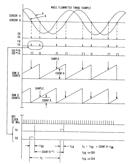
Fig. 1 shows stages in the processing of two mass
flowmeter signals in a generator in accordance with the
present invention.
Fig. 2A depicts circuit signal conditioning and
microprocessing elements of the circuit.
1322~7~
-- 3
Fig. 2B depicts latching and rate multiplying
elements of the circuit which may be connected to the Fig~ 2A
circuit.
Fig. 2C depicts programmable frequency divider
elements of the circuit which may be connected to the Fig. 2B
circuit.
Referring now to the drawings where the illustration
is for the purpose of describing the preferred embodiment of
the present invention and is not intended to limit the
invention hereto, Figures 2A, 2~ and 2~ of the drawings
together form a schematic diagram of the circuit 10 which
embodies the present invention. The circuit 10 includes a
signal conditioner 12, microprocessors 14 and 16 as shown in
Figure 2A, electronic latches 18, 20 and 22, along with bit
rate multipliers 24, 26 and 28, as shown in Figure 2B, and a
programmable frequency divider 30 as shown in Figure 2C, all
interconnected as shown.
The signal conditioner 12 receives one or more analog
signals, amplifies same, filters the signals to reduce common
mode noise and then digitizes same. The output of the signal
conditioner 12 is connected to the input to microprocessor
14. It should be noted that even though two microprocessors
(microprocessor 14 and 16) are shown, one microprocessor with
sufficient capacity can be used in place thereof.
Microprocessor 14 produces a plurality of output signals
which are transmitted to electronic latches 18, 20 and 22 via
a bus 32. The output signals from the microprocessor 14
include an enable signal to allow the transmission of bits to
latch 18, an enable signal to allow transmission of bits to
latch 20, and a control signal on bus 32. The capacity of
bus 32 is limited in that it is an 8 bit bus. Electronic
latches 18, 20 and 22 are commercially available 8 bit
latches, such as Part No. 74LS374 available from Texas
Instruments, Inc. The outputs of latch 18 are connected to
.
,
:
1322~75
the inputs to bit rate multipliers 24 and 26, and the outputs
of latch 20 are connected to the inputs to bit rate
multipliers 26 and 28. The bit rate multipliers 24, 26 and
28 are commercially available devices, such as Part No. 7497
available from Texas Instruments, Inc. A clock having an
output frequency rj is also connected as an input to each of
the bit rate multipliers 24, 26 and 28 which are
interconnected in a cascade arrangement. The outputs of bit
rate multipliers 26 and 28 are connected to a commercially
available OR gate 34, such as Part No. 74LS02 available from
Texas Instruments, Inc. The output of OR gate 34 is
connected to an input to the programmable frequency divider
30.
As previously mentioned, latch 22 receives input
signals over bus 32 from microprocessor 14. This latch also
receives a separate input signal from microprocessor 16. An
output of latch 22 is connected to the enable input to bit
rate multiplier 28. Another output of latch 22 is connected
to all of the clear inputs to bit rate multipliers 24, 26 and
28 and to an inverter 36 whose output is connected to the
clear input to the programmable frequency divider 30. A
still another output of the latch 22 is connected to the
strobe input to bit rate multiplier 28. Lastly, the
remaining outputs of latch 22 are connected to inputs to the
programmable frequency divider 30. The programmable
frequency divider 30 produces a scaled frequency output
signal indicative of the variable being measured.
Operationally, the signal conditioner 12 receives
analog signals from a device, such as mass flowmeter as
described in U.S. Patent No. 4,763,530. The flowmeter
disclosed in the foregoing patent produces two phase shifted
sine waves A and B (see Figure 1) wherein the degree of phase
shift therebetween is indicative of the mass flow rate
through the flowmeter. Thus, with such a flowmeter, the
1322~75
signals received by the signal conditioner 12 are typically
the zero crossing points of the sine waves, and the signal
conditioner produces digital signals indicative thereof.
These digital signals are transmitted to the microprocessor
14 which produces a 15 bit word proportional to the phase lag
and representative of the mass flow rate through the
flowmeter, following the steps illustrated in Figure 1. The
16th bit produced by the microprocessor 14 is a sign bit.
The microprocessor 14 also transmits an enable signal to
latch 18 allowing the first 8 bits of the 15 bit word to be
transmitted thereto over bus 32. It then disables latch 18
and transmits an enable signal to latch 20 allowing the
remaining bits of the 15 bit word to be transmitted thereto
over bus 32. Thus, the microprocessor 14 directs the
transmission of a word having a bit length that exceeds the
capacity of the bus and of each of the latches 18 and 20 by
directing the first 8 bits of the word to latch 1 and then
directing the remaining bits of the word to latch 20 all over
an 8 bit bus (bus 32). Since each bit rate multiplier 24,
26, and 28 has an input/output relationship of
rO - m x rj/26
where m has a word length of 6 bits and rj is the output
frequency of the foregoing clock, three bit rate multipliers
are required to accommodate the 15 bit word being transmitted
from the latches 18 and 20. It should be noted that,
depending upon the word length being transmitted, any number
of bit rate multipliers may be interconnected in a cascade
arrangement. Since one of the inputs to each of the bit rate
multipliers 24, 26 and 28 is a clock input frequency ri, the
output of OR gate 34 produces a signal proportional to the
foregoing clock input frequency and the mass flow being
sensed by the flowmeter.
Before any portion of the 15 bit word is transmitted
by microprocessor 16 to the latches 18 and 20, the
microprocessor 16 produces a separate 5 bit word which is
1322575
used for scaling the output of the circuit 10. The operator
can input various scaling information, e.g., upper and lower
range values, etc., into the microprocessor 16 which produces
a 5 bit word output signal representative of such and which
is utilized as an input to the latch 22. As previously
mentioned, one of the outputs of latch 22 is used to clear
the bit rate multipliers 24, 26 and 28 and to clear the
programmable frequency divider 30 via inverter 36. Another
output is utilized to enable bit rate multiplier 28. The
remaining outputs of latch 22 are connected to inputs to the
programmable frequency divider 30 which produces the desired
scaling factor (l/2n), wherein n is the rate output scale
factor and can have a value of 2 through 31. The use of such
a programmable frequency divider 30 permits scaling of the
output of the circuit 10 and improves the resolution of the
resulting output signal therefrom. With respect to the
aforementioned flowmeter, the frequency of the output signal
produced by the programmable frequency divider 30 is
representative of the flow rate passing through the flowmeter
and this output signal can be scaled, if desired, by the
operator.
Certain modifications and improvements will occur to
those skilled in the art upon reading the foregoing. It
should be understood that all such modifications and
improvements have been deleted herein for the sake of
conciseness and readability, but are properly within the
scope of the following claims.