Note: Descriptions are shown in the official language in which they were submitted.
~ 3 ~ 2 ~ `~
PNE 88 005 1 02-08-1988
Junction switch for packet switching.
The invention relates to a switching module comprising at
least one junction switch for connecting a first bus to a second bus
to transmit packetized digital information having an address field and a
data field.
A junction switch in such a switching module is used
for switching through packetized digital information in
telecommunication networks. An example in this context is a network in
which two or a plurality of computers are coupled for exchanging digital
information.
Different structures are known for the network
configuration, such as for example the Banyan network, Prelude network,
Orwell rings and the Time-division multiplex bus. Each of the said
network structures will presently be briefly discussed.
a) Banyan network.
This network is known from an article entitled
- ~Performance Analysis of a Packet Switch Based on Single-9uffered Banyan
NetworX~ from IEEE Journal on Selected Areas in Communications; VOL SAC-
- 1, No. 6; Dec. 1983, pp. 1014-1021.
The Banyan network consists of a matrix of modules each
having two inputs and two outputs. The value of an address bit from the
address field of a packet determines the output of the module to which
the packet is switched through. The output is connected to a next module
~ which switches the packet through in the same manner depending on the
; value of the next address bit. In this way a module stages are
required for an address field of a address bits. Thus, a property of
the Banyan network is the fact that the size of the network is
determined by the size of the address field and that the size of the
network cannot be designed in dependence on the traffic need.
Furthermore, it is disadvantageous that when at any
instant an equivalent address bit appears at the two inputs of a module,
` without further measures being taken, the information on that module is
blocked, disturbing the throughput. To solve such problems an intricate
.,; ~
': ~
::
3L ~3 rJ f~ ~i ~ ~
PHE 88 005 2 02-08-1988
sorting mechanism would be required for sorting and distributing packets
over the proper inputs.
b) Prelude network.
The Prelude network is known from the report of a
conference of the GSLB, held in Albufeira, Portugal, 19-20 Jan. 1987;
pp. 114-127.
A fixed number of ingoing and outgoing lines is connected
to the Prelude network. The signals on the ingoing lines are
presiochronous, that is to say, that the signals are nominally
synchronous but no longer entirely synchronous with respect to each
otheI owing to, for example, jitter and noise. In order to attain that
the input signals are bit and word synchronous, a synchronization
circuit is inserted between the ingoing lines and the rest of the
switching network.
Furthermore, additional circuitry is present for shifting
the packets with respect to each other on the ingoing lines over a time
interval having the length of an address field. Consequently, the
address fields can be transmitted to a control unit whilst being equally
distributed in time. Subsequently, the packets are further switched
through the rest of the switching network.
A disadvantageous property of the Prelude network is the
fact that the number of ingoing lines is limited (that is to say, equal
to the ratio of the number of data bits to the number of address bits);
furthermore, the ingoing lines must not function asynchronously with
respect to each other and much circuitry is required for synchronizing
the ingoing lines and shifting the packets with respect to each other.
c) Orwell rings.
This network is known from the report of a conference by
the GSLB, held in Albufeira, Portugal; 19-20 Jan. 1987, pp.215-224.
The network comprises stations that are included in a
ring-shaped bus. This ring-shaped bus comprises one or a plurality of
parallel rings. Frames containing digital information are transmitted on
each ring.
This network has the disadvantageous property that the
stations have to be synchronous with respect to each other; furthermore,
the structure of the network cannot be simply changed into a structure
different from the ring-shaped one and in addition, the user capacity
~ ` ' :' :
.~ .
PHE 88 005 3 02-08-1988
per station decreases according as more stations are included in the
ring, because there is a limitation to the user capacity of the bus.
These properties form a restriction on the possibilities to use that
network.
d) Time-division multiplex bus.
Time-division multiplex buses are widely known. A number
of ingoing data lines is connected via a multiplexer to a common time-
division multiplex bus. Each ingoing line is read out during an
associated time slot and the thus obtained data pacXet is placed onto
the common bus during that time slot. Since the time slots belong to a
fixed multiplex frame, the ingoing lines must not be asynchronous.
Each outgoing line that is connected to the common bus
has a unique address. The outgoing lines jointly read the common bus and
if a packet address field corresponds with an address of an outgoing
line the packet is copied onto the relevant outgoing line.
In addition to the disadvantage that the ingoing lines
must not be asynchronous, also high-speed buses are required when many
lines are connected.
A known routing method with telecommunication networks is
the use of virtual circuits. Virtual circuits are applied when a packet
for a specific destination should be provided with a very long world
address. To avoid this long world address, it is transmitted to a
central control unit by a station wishing to commence transmission of
the packets, which control unit establishes virtual circuits in response
thereto. These virtual circuits are formed by issuing a Virtual Circuit
Identifier, VCI for short, per section of the overall connection as well
as the required routing information for these VCI values to the
junctions in that section of the connection. These (much shorter) VCI
values substitute for the world address. The central control unit
informs each junction about the value the VCI of the arriving packet
will have and which new value the VCI of that packet is to assume to
route the packet to the next junction.
Each junction has a conversion table with a combination
of two VCI values for each virtual circuit; one VCI associated to the
arriving packet and one VCI with which that packet is to be routed
further. When a packet arrives at a junction, the VCI of that arriving
packet is looked up in the conversion table and replaced by the VCI that
., - ~
_~ J -.1 (v ~.. .~
PHE 88 005 4 02-08-1988
is associated to it according to the conversion table. Subsequently, the
packet with the new VCI is routed to the next junction. The VCI values
associated to a virtual circuit cannot be used for other circuits as
long as the virtual circuit is still in use. Only after the central
control unit has been informed that the communication can be terminated,
the VCI values of the associated virtual circuits can be released by the
central control unit.
The invention has for its object to provide a switching
module with at least one junction switch enabling a flexible network
structure, which is suitable for the implementation of the principle of
the virtual circuit and in which the input lines can be mutually
asynchronous and asynchronous relative to the output lines.
Thereto, the switching module according to the invention
is characterized in that the junction switch comprises
- a translation memory
* having a data input for receiving information words from an external
central control unit,
* having an address input to which the address field of the packets
is applied,
* and having a data output;
- a comparator
* having an input which is connected to the data output of the
translation memory, for comparing the information-word originating
from this data output to a predetermined information-word,
* and having an output;
- a queue memory in the form of an elastic buffer
* having a first data input to which the data field of the packets is
applied,
* having a second data input which is connected to the data output of
the translation memory,
* and having a write-enable input which is connected to the comparator
output for bringing the queue memory into the write position;
- an insertion circuit inserted into the second bus and comprising:
* a detection circuit for detecting available packet space on the
second bus,
* and a write circuit controlled by the detection circuit for writing
in the available packet space a packet originating from the data
..
"-,:`"
-
PHE 88 005 5 02-08-1988
output of the queue memory.
By implementing the measures according to the invention
it is achieved that the translation memory replaces an address field of
a packet by an information word indicating either a new VCI value or an
S empty-packet code. Under the control of a central control unit and vla
the data input of the translation memory this information word is
written into a memory location of this translation memory, whose address
is placed onto the address input of the translation memory by the same
central control unit. If this information word matches the empty-packet
code the writing of that packet into the queue memory is inhibited;
thus, such a packet is not switched through to the second bus, but
proceeds on its way on the first bus as do the packets that have indeed
been switched through to the second bus. If the comparator establishes
that the information word does not match the empty-packet code, the
packet carrying a new VCI value and an associated data field is written
into the queue memory and placed onto the second bus when available
packet space on the second bus is detected by the insertion circuit. By
means of this selection the junction switching function is realised.
Because the packets that have to be routed from the first
bus to the second bus first have to be placed into a queue memory and,
subsequently, must wait for available packet space on the second bus the
first bus and the second bus are allowed to be mutually asynchronous.
The network can be structured entirely according to the
traffic needs. When somewhere in the network the traffic needs are
great, many buses will be required there. With the junction switch
according to the invention the associated need for junction switches can
then be simply met. So doing it is avoided that the queue memories
overflow because the traffic supply is to big and hence information is
lost.
The switching module according to the invention is
further characterized in that the insertion circuit comprises:
- a serial/parallel register for packet information which is connected
in a series arrangement with the second bus
* having a serial data input which is connected to the load side of
the second bus,
* having a serial data output which is connected to the unload side
of the second bus,
, ~'':,' .. ' ' ., ::
. . .
. ~ : - .-
. , - i .
:......... ~ ::
. ~
-,
PHE 88 005 6 02-08-1988
* having a parallel data input,
* and having a parallel data output;
- an address length counter
* having an input which is connected to the second bus for receiving
S clock pulses from that bus,
* having a reset input which is also connected to the second bus for
receiving packet synchronization pulses from that bus,
* and having an output;
- a buffer
* having a write-enable input which is connected to the output of the
address length counter,
* having a data input which is connected to the parallel data output
of the serial/parallel register,
* and having a data output;
- a second comparator
* having an input which is connected to the buffer data output for
comparing the information word originating from this data output to
a predetermined information word,
* and having an output;
- gate means for supplying to the parallel data input of the
serial/parallel register the packet occurring at the output of the
queue memory in dependence on the signal at the output of the second
comparator.
A serial/parallel register is a register permitting both
serial and parallel reading and writing. A packet on the second bus is
serially written into the serial/parallel register.
With the aid of the address length counter the address
field of a packet position on the second bus is written in parallel into
the buffer memory and with the aid of the second comparator it is
detected whether this address contains the empty-packet code, so that
this packet position can be filled with a packet from the queue memory.
The switching module according to the invention is
further characterized in that the junction switch comprises a second
and a third buffer which are serially connected to the first and the
second bus, respectively, the second and the third buffer comprising a
clock input connected to the respective clock channels of the first and
; the second bus, and a reset input connected to the clock input through a
:
` ` : `` :
`:
:~' ` . '` .. ~'
7 28381--5
delay element.
Buffers are placed on the respectlve unload sldes of the
first bus and the second bus. These buffers are used for ellml-
natlng phase differences between the packet bits and the clock
bits, which phase differences may be lntroduced by the ~unction
switch. Furthermore, this achieves that the duratlon of the clock
pulses malntains substantially the same value, so that it ls lm-
posslble that owing to the accumulatlon of the pulse duratlon a
clock period would be completely filled by one clock pulse, so
that one clock period would be skipped.
The invention and lts advantages wlll now be further
explalned with reference to the drawings, in whlch:
Flg. 1: shows a dlagram of a packet-swltched network
operatlng wlth vlrtual clrcults,
Flg. 2: shows a dlagram of a swltchlng module wlth
~unctlon swltches accordlng to the lnventlon,
Flg. 3: shows a clrcult dlagram of a ~unctlon swltch
accordlng to the lnventlon.
In packet-swltched communlcatlons vlrtual clrcults can
be used of whlch an example ls shown ln Flg. 1.
It ls assumed that termlnal statlon 1 wlshes to transmlt
lnformatlon to termlnal statlon 2. Each termlnal statlon ln thls
network ls characterlzed by a unlque world number that, ln analogy
wlth the already exlsting telephone network, can conslst, for
example, of a subscrlber number and posslbly an area code and a
country code. In order to avold that a long world number leads to
an extremely long packet address, a central control unlt 4 forms
;~ r~; .~ ~J . .~'
7a 28381-5
vlrtual circults comprlslng the respectlve ~unctlons 3-1, 3-2 to
3-n between termlnal statlon 1 and termlnal statlon 2, the central
control unlt 4 asslgnlng to the lnter~unctlon connectlons the re-
spectlve VCI (VCI = Vlrtual Clrcult Identlfier~ values 5-1, 5-2,
5-n-1. When junctlon 3-1 recelves a packet from terminal statlon
1, junctlon 3-1 routes thls packet to ~unctlon 3-2 havlng VCI
value 5-1. Junctlon 3-2 looks up the value 5-1 ln lts converslon
table and flnds there the value 5-2. The packet ls then routed to
VCI value 5-2. Flnally, thls packet arrlves at ~unctlon 3-n hav-
lng VCI value 5-n-l. In the converslon table of ~unctlon 3-n lt
ls stated that arrlvlng packets havlng the VCI value 5-n-l are to
be routed to the exlt whlch ls connected to the termlnal statlon
2.
PHE 88 005 8 02-08-1988
Since the junction switch according to the invention
comprises a translation memory capable of translating the address codes,
this junction switch is pre-eminently suitable for use in virtual
circuits.
Fig. 2 shows a switching module having _ ingoing buses
referenced 1 to _ and _ outgoing buses referenced n+1 to n+m.
For each communication between one of the n ingoing
,~'`r~ buses and one of the m outgoing buses a junctionvcr switch is always
used whose input is connected to the associated ingoing bus and whose
output is connected to the associated outgoing bus. These junction
switches are used for routing the digital information through the
network.
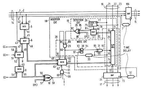
Fig. 3 shows an embodiment of a change-over switch
according to the invention. The unload side of a first bus 14
accommodates a buffer ~
This bus 14 comprises three conductors 1, 2 and 3,
conductor 1 being used for conveying the packet synchronization signal
for the packets which are transmitted via conductor 2 of the first
bus 14. These packets consist of an address field and a data field. The
conductor 3 conveys the clock signal for the bit synchronization on
conductors 1 and 2 and is connected via a time delay element 7 to the
~ 't
reset input of buffer ~. The descending edge in a clock pulse is then
related with a fixed time to the ascending edge so that the clock pulse
cannot fill a complete clock period as a result of various mutual delays
! 25 in the ascending and descending edges.
The conductors 2 and 3 are connected to data input 41 and
clock input 42, respectively, of the register 5. The packets are bit-
serially read into the register 5.
The conductor 1 is connected to the write-enable input 43
of buffer 6. The data input 45 of the buffer 6 is connected in a
~ . .
parallel arrangement with data output 44 of register 5, so that a packet
in register 5 is written in parallel into buffer 6 in dependence on the
packet synchronization signal on conductor 1.
A first data output 46 of buffer 6 is connected to data
input 48 of queue memory 12 to enable a packet data field to be
written in parallel into the queue memory 12; the other data output
47 of buffer 6 is connected to data input 49 of multiplexer 8 for
-
.
: - - . ~ .,
: : ~
: ' '
,,, " ~
PHE 88 005 9 02-08-1988
transmitting thereto in parallel a packet address field. This
address field forms a VCI value. Multiplexer 8 has a bit-parallel output
52 which is conne~ted to the address input 53 of translation memory 9. A
parallel data input 50 of multiplexer 8, a selection input 51 of
multiplexer 8 and a data input 54 of translation memory 9 are coupled to
the central control unit CC.
The parallel data output 55 of translation memory 9 is
connected to input 56 of comparator 10 and a predetermined information
word EPC1 indicating an empty packet is applied to the other input 57 of
comparator 10. The parallel data output 55 of translation memory 9 is
also connected to data input 57 of queue memory 12. The output 58 of
comparator 10 is connected to input 60 of AND gate 11 whose input 59 is
connected to conductor 1 of bus 14 for the packet synchroni~ation. The
output 61 of AND gate 11 is connected to the write-enable input 62 of
queue memory 12.
Via data input 49 of multiplexer 8 a VCI value coming
from buffer 6 and vla data input 50 of multiplexer 8 a memory address
coming from the central control unit CC can be conveyed to the address
input 53 of translation memory 9. Depending on the value of the
selection signal at selection input 51 of multiplexer 8 either the VCI
value from buffer 6 or the memory address is applied to the address
input 53 of translation memory 9. If a memory address coming from the
central control unit CC is delivered, an information word forming a new
VCI value Ol denoting an empty packet is written into the translation
memory at the address concerned. If a VCI value coming from buffer 6
is applied to the address input 53 of translation memory 9, the
information word is read out at the address concerned and appears at
data output 55. This information word is then applied to input 56 of
comparator 10 and data input 63 of queue memory 12. Comparator 10
compares the information word at input 56 to the empty packet code
EPC1 which is delivered to input 57 of comparator 10 and if they do not
match, the write-enable input 62 of queue memory 12 is activated vla AND
gate 11. This results in the new VCI value and the associated data field
being written in simultaneously vla the respective data inputs 48 and
63 of queue memory 12. If comparator 10 establishes that the data word
: and the empty packet code EPC1 match, the write-enable input 62 of queue
memory 12 is not activated. This is the case with packets that need not
: .: ~ ,.
.
.:::: .
~ " ~.:: .
~ ~ - : .:
PHE 88 005 10 02-08-1988
be switched through from bus 14 to bus 17 on the basis of their
destination. The address field and the data field at the respective data
inputs 48 and 63 of queue memory 12 are now discarded.
The packet which is written into queue memory 12 is
switched through to the second bus 17 by an insertion circuit 18. This
insertion circuit 18 comprises a detection circuit 19 for establishing
the presence of free packet space on the second bus 16 and a write
circuit 20 for writing in that case a packet from queue memory 12 into
the empty packet space. On the unload side of the second bus 16 a buffer
24 is arranged. This bus 16 comprises three conductors 21, 22 and 23, of
which conductor 21 is used for transporting the packet synchronization
signal for the packets that are transmitted from bus 16 vla conductor
22. Conductor 23 conveys the clock signal for the bit synchronization of
the packets on the conductors 21 and 22 and, vla delay element 32, is
connected to the reset input 73 of buffer 24. This is done to avoid a
clock period being skipped in the clock signal as is represented with
reference to the description of buffer 4. The conductors 21 and 23 are
directly connected to buffer 24 and conductor 22 is connected to buffer
24 vla serial/parallel register 25.
The serial/parallel register 25 comprises a serial data
input 71 connected to the packet conductor 22, a parallel data input 74
connected to data output 81 of queue memory 12, a write-enable input 75
connected to output 82 of AND gate 31, a serial data output 72 connected
to packet conductor 22 and a parallel data output 76 connected to data
input 83 of buffer 27.
The conductor 21 is connected to reset input 77 of
counter 26 and conductor 23 to clock input 78 of the counter 26. The
output 79 of counter 26 is connected to the write-enable input 80 of
buffer 27.
The parallel da~a output 84 of buffer 27 is connected to
input 85 of comparator 28. A predetermined information word EPC2,
denoting an empty packet code, is applied to the other input 86 of
comparator 28. The output 87 of comparator 28 is connected to input 88
of AND gate 29 whose input 89 is connected to queue-empty output 91 of
35 queue memory 12. The output 90 of AND gate 29 is connected to the read-
enable input 92 of queue memory 12 and set input 93 of FLIP-FLOP 30.
The reset input 97 of FLIP-FLOP 30 is connected to packet
.
:~
PHE 88 005 11 02-08-1988
conductor 21 vra a delay gate 33. AND-gate 31 has two inputs 95 and
96, input 95 of which being connected to output 94 of FLIP-FLOP 30 and
input 96 of which being connected to packet synchronization conductor
21.
The packets on conductor 22 are bit serially applied to
data input 71 of serial/parallel register 25. The counter 26 counts the
number of bits from the packet synchronization pulse, which is serially
applied to serial/parallel register 25 until the complete address field
of a packet is written into serial/parallel register 25. Subsequently,
under the control of a write-enable signal on write-enable input 80 of
buffer 27 the address field is written in parallel into buffer 27.
Comparator 28 compares the address field in buffer 27 to empty
packet code EPC2. If the address field at input 85 is equal to the empty-
packet code EPC2 at input 86 of comparator 28 and also queue memory 12
comprises a packet, the output signal of AND gate 29 activates the read-
enable input 92 of queue memory 12 to read out the next packet in queue
memory 12. The output signal of AND gate 29 is likewise applied to set
input 93 of FLIP-FLOP 30 so that a take-over signal appears at output 94
of FLIP-FLOP 30. As this take-over signal is presented at output 94 of
FLIP-FLOP 30 and a packet synchronization pulse at input 96 of AND gate
31, write-enable input 75 of serial/parallel register 25 is activated.
The delay gate 33 which is connected to the reset input 97 of FLIP-FLOP
30 has a delay amounting to approximately a half clock pulse. With this
delay it is avoided that the take-over signal at output 94 of FLIP-FLOP
30 has changed value before the write-enable input 75 of serial/parallel
register 25 can be activated by means of the take-over signal and a
packet synchronization pulse on the respective inputs of AND gate 31. At
the instant when the packet bit positions in serial/parallel
register 25 match the packet bits on the parallel data input 74, the
packet on output 81 of queue memory 12 is written in parallel into
serial/parallel register 25. This achieves that a packet on bus 14 is
routed to bus 17, thus realising the junction function of the switch.
`:
`:
-
.. ~