Note: Descriptions are shown in the official language in which they were submitted.
MASK REPAIR ~ 3 L~
Back~round of the Invention
Technical Field
This invention relates to the fabrication of lithographic masks and, in
5 particular, the fabrication of lithographic masks utilized in device fabrication.
Art Back~round
In the fabrication of devices, e.g., semiconductor devices, magnetic
bubble devices or opdcal devices, it is generally necessary to configure on a
substrate a region (e.g., a metal, semiconductor or dielectric region) in a specific
10 spatial pattern and location. (A substrate is a mechanically stable body including,
e.g., semiconductor regions and/or metal regions and/or dielectric regions.) Theposidoning and/or patterning of these regions is generally accomplished by a
lithographic process. In this process a mask is udlized to image energy in the
desired pattern onto a substrate surface that has been coated with a material
15 sensidve to the incident energy. The mask in this exposure step is generally
placed in contact with or in close spadal reladon to the substrate. Alternatively,
the mask pattern is projected onto the substrate.
After exposure, development of the energy sensidve material is
performed to selecdvely remove either the exposed, or unexposed regions, of the
20 resist material. (For a negadve resist the unexposed region is removed while for a
positive resist the exposed region is removed.) Generally, a solvent or energetic
entities from a plasma are employed to effect this removal. The resulting,
patterned energy sensitive material, i.e., resist, is employable as a processirlg mask
for accomplishing the processing, e.g., selecdve doping, etching, oxidizing of or
~5 deposidon onto the underlying substrate regions.
The mask udlized for exposure of the resist material generally
includes a patterned metal or metal oxide film. Materials such as chromium,
chromium oxidc, tungsten or nickel are typically used for photomasks. These
matcrials arc commonly formed in a layer thickness of approximately
30 500 Angstroms to 1000 Angstroms for photomasks on a transparent substrate such
as a quartz glass substrate. (In the context of this disclosure, the terrns transparent
and opaque refer to the energy that is effecdve in inducing reacdon in the resist
material to be exposed. For a material to be considered opaque, it should transmit
less than 10 percent of this energy while for the material to be considered
35 transparent it should transmit at least 80 percent of this energy.) The metal or
metal oxide film of the mask is typically manufactured by deposidng a resist
,
. ~
, ~
~ ~ .
~ 3 ~, j, ;; i
material sensitive to electrons onto its surface, exposing this resist material with a directed
electron beam, and developing the exposed resist to form the desired pattern (see, D.J. Elliott,
Inte~rated Circuit Fabrication Technoloev, McGraw-Hill, New York, 1982, for a description of
the fabrication of photomasks.
In the manufacture of masks, transparent defects such as pin holes or entire
missing portions often occur. These defects, in turn, cause defects in the integrated circuit or
other device produced when using the mask. Since the manufacture of masks is generally a
time-consuming and relatively expensive operation, it is often desirable to repair a defective
mask by selectively forming an opaque material on the unwanted transparent region. The
repair procedure is, however, not acceptable unless it is less costly than merely producing
another mask. The repair should also produce an opaque deposit that is sufficiently adherent
to the mask substrate that subsequent processing and cleaning during mask fabrication or
during subsequent use of the mask does not induce loss of the repaired material. Additionally,
the resolution of the repair procedure should be at least as good as the desired resolution of
the mask itself to avoid mask and, in turn, device degradation.
A variety of processes have been disclosed for effecting repair of transparent
defects. In a known procedure, a laser is utilized to expose a metal ink on the mask surface.
Although this procedure has been found quite efficacious for repair of masks formed with
design rules of 1 ~m or larger, repair of masks with finer design rules, e.g., 1 ~m or finer, is
2 0 more difficult. (A design rule is the feature size for the smallest feature (line or space) that
must be delineated by the mask to form the desired device). Another procedure, formation of
carbonaceous films utilizing a focused ion beam, has also been discussed in H.C. Kaufman,
W.B. Thompson, and G.J. Dunn, Proceedines of SPIE, International Society of Optical
Engineering, ~, 60 (1986) and M. Yamamoto, M. Sato, H. Kyogoku, K Aita, Y. Nakugawa,
2 5 A. Yasaka, R. Takusawa, and O. Hattori, Proceedines of SPIE, International Society of
Optical Engineering, ~, 97 (1986). However, essentially no details have been given
concerning the conditions or materials utilized and these processes have been difficult to
reproducibly control.
~ .
~ummary of the Invention
A rapid, expeditious procedure for forming an adherent opaque deposit in the
repair of masks having design rules of 1 ~m or finer is accomplished utilizing an ion beam
technique. In this process an ion beam, including heavie:r metal ions, e.g., ions of atoms such
S as gallium, lead, indium, and gold, are utilized to impact the region of the mask to be
repaired in the presence oE an organic material. The organic material is introduced in the
vapor phase and should include a composition having an unsaturated substituent bound to an
aromatic ring or aromatic ring system. For example, organic materials such as benzoEuran,
indene, phenylacetylene, and styrene yield desirable results. In contrast, if a material that
does not have an unsaturated moiety attached to an aromatic ring or aromatic ring system is
utilized, such as benzene, toluene or methylmethacrylate, the material either does not form
as a deposit or the resulting deposit is translucent.
The metal such as gallium from the ion beam induces a heterogeneous
reaction in the impacted gas to produce a carbonaceous material that includes the metal
entity. The resolution of this metal-containing deposit is commensurate with the spot size of
the ion beam. The procedure is rapid and for appropriately chosen organic materials the
deposition process is not excessively sensitive to the dose rate of the metal ion beam. The
resulting deposit is opaque to exposing energies such as visible radiation, ultraviolet radiation,
deep ultraviolet radiation, ion beams, and electron beams.
In accordance with one aspect of the invention there is provided a process for
fabricating a patterned mask suitable for use in the lithographic fabrication of a device
comprising the steps of forming a pattern for said mask, and repairing a transparent defect in
said pattern characterized in that said repair is performed by impacting the region of said
mask containing said defect with a metal ion beam in the presence oE an organic gas to
establish an opaque material contributing to a deposit remaining after said impacting wherein
said organic gas comprises an organic compound having an unsaturated substituent bound to
an aromatic ring or ring system such that said metal ion beam at said region induces a
chemical reaction in said gas that results in said opaque material deposit, wherein said
deposit includes entities oE said metal and wherein said ion beam has a current density oE at
least 0.1 amp/cm2.
~ 3 ~"~
In accordance with another aspect of the invention there is provided a mask
comprising a patterned layer on a substrate, said pattern comprising a primary material and a
region of a composition adherent to said material or to said substrate wherein said
composition comprising a carbonaceous material that includes a metal entity.Brief
5 DescriPtion of the Drawin~s
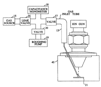
FIG. 1 is illustrative of an apparatus suitable for practising the invention, and
FIGS. 2 through 5 are illustrative of results obtained by such practice.
Detailed Description
Repair of a mask such as a photomask (e.g., an ultraviolet photomask or a
10 deep UV photomask) as well as an electron or ion transmission mask is effected by
impacting in the region to be repaired an organic material with ions of heavier metals. The
gaseous material employed should include an aromatic ring or aromatic ring system with a
substituent having an unsaturated bond, e.g., a vinyl or acetylenic bond. Suitable materials
include benzofuran, indene, phenylacetylene, and styrene. For convenience, the source of
15 the gaseous material should either be a gas or a material having a vapor pressure sufficiently
high to allow introduction of a vapor into the region of the mask to be repaired. Generally,
inlet pressures in the range 0.5 to 5 Torr are utilized. The size of the
-3a-
~ ~,1 '"~, ', ' ,
chamber does not substantially affect the desired inlet pressure provided the
distance between the inlet and the region to be repaired is less than the internal
diameter of the inlet tube. Typically, inlets with inner diameters in the range
25 llm to 1 mm are useful. The spacing is conveniently established by
5 positioning the inlet the desired distance above the mask and translating the mask
so that the area to be repaired is directly in the flow direction. Typically, toproduce the desired flow rates, vapor pressures above 0.5 Torr are desirable. If a
material that does not have an unsaturated bond in conjunction with an aromatic
ring is employed, the resulting deposit either does not form such as in the case of
10 benzene or toluene or the deposit is not opaque such as in the case of
methylmethacrylate.
The deposit of repair material occurs in the region of the mask
impacted by the metal ion. The deposition essentially does not spread beyond theimpacted area. Thus, the resolution of the deposited material depends on the spot
15 size of the ion beam, i.e., the diameter (or for non-circular spots the diameter of a
circle having an equivalent area) of the region encompassed by the full width athalf maximum of the beam current spatial profile. Typically, ion beam spot sizessmaller than 0.5 microns, indeed as small as 0.05 micrometer, are presently
achievable. (See, L. Harriott, Proceedin~s of SPIE, 773 (1987), for procedures
20 and equipment suitable for producing metal ion beams having these spot sizes.)
Typically, acceleration voltages for the ion beam in the range S to 50 KeV is
employed. Acceleration voltages below S KeV lead to excessive spot diameter
while acceleradon voltages above 50 KeV typically result in substandal
implantadon of ions into the mask.
To form a suitable deposidon, the metal interacts with the organic
material inducing reacdon of the gas to form a carbonaceous deposit that includes
at least a pordon of the metal. Generally, ions of heavier metals such as gold,
indium, gallium, and lead result in suitable deposidon. Typically, the metal is
present in the repair material at a concentradon between 10 and 30 atomic percent
30 At concentradons substantially less than 10 atomic percent there is an undesirable
loss of opacity.
The reacdon essendally does not occur in the gas phase and is
essentially entirely a heterogeneous reacdon at the substrate surface. Thus, theextent of final deposition is determined by 1) the adsorption rate of the gas at the
35 substrate, 2) the dose rate of the incident ions, 3) the sputtering rate, i.e., the rate
of removal of the deposited material, and 4) the polymerizadon rate which, in
turn, depends on the gas precursor.
- 4 -
1 ~,` ,: ,. : ,
The rate of ~ormation of the repair material (as determined by the
factors 1), 2), and 4)) should be greater than the rate of sputtering induced by the
impacting ions. Typically, this result is achieved by utilizing organic gas flowrates in the range 10 to 10 molecules/cm -sec in conjunction with ion dose
5 rates in the range 1018 to 1019 ions/cm2-sec. The molecular flux should
advantageously be higher than the ion flux. (Molecular fluxes in the range 1018
to 10 molecules/cm -sec are advantageously achieved by employing the
previously discussed inlet pressures.) Typically, to.maintain a suitable deposition
relative to sputtering rate, it is desirable to utilize multiple passes of the ion beam
10 through the area to be repaired. In this manner, it is easier to ensure that the
arrival rate of ions for typical beam current densities, i.e., densities in the range
0.1 to 1 amps/cm, is suitable for the typical gas flows discussed above.
Generally, only 1 to 10 passes with scan rates of 0.1 to 1 ~lm /sec is required to
produce an opaque deposit. These parameters correspond to a rate of
15 approximately 10 ~sec to 10 millisec per pixel. Thus, rapid scanning, i.e.,
scanning faster than 10 llsec/pixel, that often leads to loss of resolution and
placement accuracy for the deposited material is avoided. (A pixel is half the full
width at half maximum of the beam current spatial profile.) The extent of deposit
depends on the total dose employed. Generally, sufficient material for opacity is
20 deposited with a total dose in the range 1017 to 1018 ions/cm2.
The following examples are illustrative of suitable conditions for the
practice of the invention.
Example 1
The apparatus of FIG. 1 was utilized to repair a mask. The apparatus
25 included an ion source, collimator and lens. This ion beam equipment was
described in L. Harriott, Proceedings of SPE, 773 t1987). Standard acceleration,collimating, and focusing equipment were utilized. A gas inlet tube, 13, was
introduced into the deposition chamber and positioned so that its end was
approximately 100 microns from the point where the ion beam strikes the sample.
30 The angle of the gas inlet tube was adjusted to make an angle of approximately
22 degrees relative to the major plane of the mask. The gas source, 15, includeda gas bulb that was suitable for holding a liquid source of the reactant to be
utilized. A leak valve, 16, and a valve, 17 was supplied for controlling the flow
of this reactant to the mask to be repaired. A capacitance monomer, 18, was
35 utilized to monitor gas pressure and a roughing pump, in conjunction with valve,
20, was utilized to evacuate the reactant supply system.
:' ' I '
In operation, a cryogenic pump was utilized to evacuate chamber, 40,
to a pressure of approximately 10-7 Torr. Utilizing a load lock system, a
chromium mask having a variety of lines and spaces with the smallest space beingapproximately 1 micron was positioned on the sample holder, 21. The roughing
S pump, 19, was activated while valves, 16 and 17 were closed. Approximately
2 milliliters of research grade styrene was introduced into the gas source tube, 15.
The tube was then immersed in liquid nitrogen. Valve, 16, was opened to remove
any air present in the gas source system. The liquid nitrogen was then removed
and the leak valve, 16, was closed when the styrene began to melt. This
10 procedure of freezing and air removal was repeated a second time. Valve, 20, was
closed, valve, 17, opened and valve, 16, adjusted so that the capacitance monomer
read a pressure of 2 Torr of styrene.
A gallium ion beam (beam current of 0.5 amp/cm2) was focused at
the mask surface. The focused beam was then utilized to position the mask
15 portion to be repaired directly in the beam path. The beam was also utilized to
position the gas inlet tube at the position described previously. (This positioning
of the substrate and of the inlet tube is performable either before or after thestyrene flow is initiated. Since a rapid scan is utilized for positioning, even with
the styrene present a negligible amount of deposition occurs.) The region to be
20 repaired measured approximately 2 by 10 microns and was scanned at a rate of
approximately 10 milliseconds per pixel with 10 passes being utilized. The ion
beam was then terminated, the leak valve, 16, was closed, and the system again
evacuated utilizing roughing pump, 19, and the cryogenic pump present on
deposition chamber, 40.
Using this repair procedure the scan rate was varied in a series of
exposures to yield total doses in the range 1 to 5X10¹⁷ ions per centimeter square.
The relationship of total dose to the film thickness obtained is shown in FIG. 2.
The samc series of depositions were repeated and the percent transmission of thedeposit depending on the dose being utilized is shown in FlG. 3. One of the films
30 produced by the above-described procedure having a thickness of approximately200 Angstroms was subjected to Auger depth profiling. The results are shown in
FIG. 4. It should be noted that for extremely thin films (200 Angstrom films) the
gallium concentration is somewhat lower than is typically obtained for thicker
films. That is, the gallium concentration is approximately 10 atomic percent as
35 opposed to a more typical 20 to 30 atomic percent, as shown in FIG. 5, for a film
thickness of 2000 Angstroms. The 200 Angstrom deposited film was sufficiently
thin to still be essentially transparent. Thus, thicker films are typically required to
- 6 -
produce a suitable opacity. (The Auger and thickness experiments were perforrnedfor repairs having significantly larger feature sizes, e.g., approximately
100 microns, so that the resolution of the measuring equipment was not
exceeded.)
5 Example 2
The procedure of Example 1 was followed except individual runs
were performed utilizing benzofuran, indene, and phenylacetylene rather than
styrene as the gaseous reactant. In each case, the results achieved were essentially
identical to that of Example 1. For some of these gases, because of their
10 relatively low vapor pressure, the partial pressure utilized during deposidons was
somewhat lower than 2 Torr.
Examplè 3
The procedure of Example 1 was utilized except runs employing
methylmethacrylate, benzene, and toluene were performed. For the benzene and
15 toluene runs no noticeable deposition occurred even when the number of passeswas increased to 1000. Indeed, some of the mask substrate was removed due to
sputtering processes. For methylmethacrylate, deposits were obtained, however,
these deposits were transmissive and the opacity was not substantially increasedeven with significant increase of total dose.