Note: Descriptions are shown in the official language in which they were submitted.
The present invention relates to the fabrication of
electronic circuit packages and in particular to methods, and
mechanical means for attaching electronic components,
especially leadless ceramia packages for electronic devices,
to each other or to supporting substrates such as circuit
boards.
The microelectronics lndustry is steadily moving toward
the use of smaller electronic circuit devices giving rise to
the need for smaller and smaller connecting devices and
mounting means for the circuit devices. Circuit devices,
such as integrated circuits of complex nature, are embodied
in large chips and chip carrier packages (CCP) which have
connection pads on the faces and/or edges of the packages.
Chip carrier packages can be produced with leads attached
(leaded) or they can be leadless.
Leaded CCP's can be soldered directly onto printed
circuit boards or printed wire boards. Leadless CCP's can be
soldered onto ceramic boards or installed into connectors.
However, with glass/epoxy printed circuit boards or othar
printed wiring boards (hereinafter substrates) leadless CCP's
are usually mounted into connectors which are, in turn,
mounted on the substrates because of the effect of different
thermal expansion coefficients of the materials involved when
subjected to temperature fluctuations. Specificallyl the CCP
and the substrate exhibit
-- 1 --
~,
.
,
.
`
' ,
'
~ ~1 2 f~
--2--
different thermal characteristics leading to in-plane
stress and strain therebetween as a result of thermal
mismatch. Also, any flexure of the substrate result in
out-of-plane stresses. Prior art techniques have used
small solder sphere~ or solder paste to attach packages
to sub~trates. Although such known techni~ues have been
used ~or such surface mounting, there exists a need for
a compliant solder joint to compensate for the large
stresses resulting from thermal mismatches between the
CCP and the substrate, as well as from board warpage
and flexure.
Different solutions have been proposed for the
foregoing problems. The proper positioning of a prede-
termined quantity of solder may be achieved with the
use of solder preforms spaced on a carrier template in
the locations corresponding to the points where the
solder joints are to be formed, Examples of this tech-
nique may be found in U.S. Patents 3,320,658, issued to
Bolda et al; 3,396,894, issued to Ellis; 3,472,365
issued to Tiedema; 3,719,981 issued to Steitz;
3,744,129, issued to Dewey; 4,209,893, issued to Dyce
et al; and 4,216,350, issued to Reid.
Although the foregoing techniques provide for
the correct placement of a predetermined quantity of
solder or other suitable joint-forming material, and
with the proper dimensioning of the carrier or template,
sufficiently small quantities of solder can be posi-
tioned on close spacing between centers, these propo-
sals do not address the problems of high shear strains
in the solder joints.
In U.S. Patent No. 4,412,642 to Fisher,
leadless chip carriers are converted to '~cast-leaded
chip carriers" by molding high melting point leads to
the chip carrier. Additional examples of methods and
. .
~ , ; : . ,, : '
. .
~ ' ' ` ~ ' . , ' , ~ ', :
1~2~ '3
devlces for soldering terminals to a printed circuit board
are shown in U.S. Patent No. 3,926,360 to Moister and in the
IBM Techical Disclosure Bulletin, Vol. 21, No. 6, dated
November 1978.
While the above disclosures have addressed the problem
of connections which must be able to withstand the stresses
from thermal cycles, none discloses a satisfactory solution
which both solves the problem and is suitable for reliable
manufacturing processes.
Because of the significant problems associated with the
attempt to position preferred material such as a solder and --
to effect electrical contact, alternative less desirable
conductive materials and/or mechanical approaches have been
developed. U.S. Patent 4,064,623 to Moore shows an
electrical connector utilizing conductive rubber rods. U.~.
Patent No. 4,295,700 to Sado discloses a similar press-
contact type interconnector utilizing elastic material having
anisotropical electroconductivity. U.S. Patent No. 3,991,463
to Squitieri et al, diæcloses a method of forming an
interconnector having a row of electrically conductive
flexible plastic strips. U.S. Patent No. 4,027,936 to Nemoto
et al discloses a connector having electroconductive rubber
terminals. U.S. Patent No. 4,144,648 to Grovender, discloses
a connector utilizing conductive elastomer medium. U.S.
Patent No. 4,402,450 to Abraham et al, discloses contact pads
of a device which are adapted for bonding components such as
contacts of a circuit assembly thereto.
Unfortunately, none of the above disclosures provide the
superior electrical interconnection accomplished by solder.
It wsuld therefore be highly desirable to have a solder
preform delivery system
-- 3 --
~.
, . .
:
, . , ~
~, , .
.
~922$~
with a precise placement of a predetermined quantity of
material in a preferred geometric preform for the formation
o~ a solder-type connection.
Commonly assigned published U.K. patent application GB
2,142,~68 A to ~llen et al, discloses a chip carrier mounting
device which includes a retaining member having a defined
pattern of apertures in which are positioned preforms of
joint-forming material such as solder or conductive
elastomer. The instant invention is an improvement to that
mounting device wherein the problem of solder preform
positioning and solder preform configuration are addressed.
In one aspect, the invention provides a solder post
delivery system comprising: a positioning means for
positioning solder posts, said positioning means being
elongated along a longitudinal axis, said positioning means
having a plurality of longitudinally spaced openings
therethrough, each of said openings having a top and a bottom
generally parallel to said longitudinal axis wherein said
2Q positioning means is folded along a line generally parallel
to the tops and bottoms of said openings providing
unobstructed access to said solder posts; an elongated and
flexible backing means having at least one adhesive surface,
said backing means connected to said positioning means by
said surface and to solder posts to be positioned through
said openings; and a plurality of solder posts positioned by ~-
said openings and held therein by said backing means, said
positioning means capable of being bent with respect to said
longitudinal axis to align the ends of said solder posts with
respect to electrical components to be interconnected.
In preferred embodiments of this aspect, the invention
provides~ '
~ !
.
.'. 1," , ~ `. ' ', ' :
,, ., ' ~ . ' , ~
3 ,~ f ~
--5--
The above delivery system wherein longitudinal ends of
said positioning means are closed into a loop which is
capable of bein~ curved outwardly to conform to a geometric
5 configuration and is capable of being retai.ned in said
configurat.ion for intercon~ec~ion of said solder posts; an~
wherein said loop is capable of being bent from a generally
circular cross-section to a generall~ rectangular cross~
section.
The above delivery system wherein said backing means
includes an adhesive surface on both sides thereof, said
positioning means capable of being placed against external
support and being retained in position by said backing means.
The above delivery system wherein said positioning means
is folded along a line passing generally midway between the
tops and bottoms of said openings providing unobstructed
access to said solder posts, said backing means extending
beyond at least one longitudinal periphery of said
positioning means to provide a surface for securing said
positioning means.
The above delivery system w~erein said positioning means
is folded along lines coincident with the tops and bottoms,
respectively, of said openings to form a Ushaped cross-
section having top and bottom flanges that extend
transversely at right angles to said longitudinal axis; and
wherein at least one. of said flan~es is provided with at
least one notch, said adhesive surface o~ said backing means
being exposed through said notch; and further including cover
means in removable contact with said exp~sed adhesive surface
to protect said surface before installation of said system;
and wherein said flanges are cut transversely to allow said
positioning means to be bent.
,
,:
~ : ' ' ' ''
1 3 ~ ?~
--6--
The above delivery system wherein said positioning means
is folded along a line coincident with tops of said openings
to form an L-shaped cross-section having a top flange that
extends transversely at a right angle to said longitudinal
axis, said backing means conforming to said top flange to
provide an adhesive surface capable o~ securing said
positioning means with respect to a substrate; and wherein
said flange is cut transversely to allow said positioning
means to be bent; and wherein said flange includes at least
one window opening therethrough, said adhesive surface being
exposed through said window opening; and further including
cover means in removable contact with said exposed adhesive
surface to protect said surface before installation of the
system.
The above delivery system wherein at least two of said
openings are empty and said positioning means is folded
transversely with respect to said longitudinal axis between
said two openings, said adhesive surface of said backing
means extending through each of said two openings to contact
itself to define a tab and a corner for said positioning
means.
In a further aspect, the invention provides a solder
post delivery system comprising: a positioning means for
positioning solder posts, said positioning means including at
least three layers of sheetlike material, each of said layers
having a plurality of openings therethrough, the openings in
each layer being in general axial alignment with the openings -
in the other layers, said openings being capable of being ~ --
slightly misaligned by movement of the layers with respect to
each other; and a plurality of solder posts, one solder post
being positioned in each generally aligned opening and being
secured therein by a force fit created by said slight
.,~.
., . . ~ ~
--7--
misalignment.
In a preferred embodiment of this aspect, the invention
provides:
The above system wherein said positioning means is slit
through said layers and said layers are bent slightly out of
the plane of said layers to define abutmant means for contact
and alignment of electrical components to be interconnected
by the system.
In a still further aspect the invention provides a
solder post delivery system comprising: a positioning means
for positioning solder posts comprising a ~ontinuous frame
having an inner and outer periphery, said frame capable of
being discontinuous, said positioning means having securing
portions which are capable of removably securing solder posts
thereto when said frame is continuous and which are capable
of releasing solder posts that may be secured thereto when
said frame is discontinuous; and a plurality of solder posts
in contact with said securing portions of said positioning
means; and wherein said frame has a generally U-shaped cross-
section having top and bottom flanges and a securing portion
on the inner periphery of said frame comprising a plurality
of spaced openings, each of said openings extending across
the width of said inner periphery and into said top and
bottom flange, each of said solder posts being positioned and
held within one of said openings by contact with the edges of
each of said openings.
The invention also provides:
A solder post deli~ery system comprising: a positioning
means for positioning solder posts comprising a continuous
~'~
.
,
~ ~ ~ rr~ r ,~
~rame having an inner and outer periphery, said frame capable
of being discontinuous, said positioning means having
securing portions which are capable of removably securing
solder posts thereto when said frame is continuous and which
are capable o~ releasing solder posts that may be secured
thereto wh~n said ~rame is discontinuous; and a plurality of
solder posts in contact with said securing portions of said
positioning means; and wherein the inner periphery of said
frame is contoured to provide spaced securing portions
thereof that are complementary to said solder posts to secure
said solder posts thereto, said frame having corners, said
frame being dis~ontinuous at one of said corners of said
frame including separate removable fastening means to hold
said corner together, said other corners being bendable in
hinge-liXe fashion to open said frame with respect to said
solder posts to release said solder posts from said securing
portions.
A solder delivery system comprising: a positioning
means for positioning solder posts, æaid positioning means
having a plurality of openings therethrough; and a plurality
of solder posts with one post per opening, said posts
comprising solder paste which fills said openings to define
individual solder posts: and wherein said positionin~ means
and said solder paste are co-extruded in one direction to .
define a continuous composite, said composite being sliced ::-
thxough at an angle perpendicular to the direction of co-
extrusion to define an individual solder delivery system.
A solder posk delivery system comprising: a positioning
means for positioning solder posts, said positioning means
being generally planar and having a plurality of openings
therethrough, said positioning means being made from a heat
recoverable polymeric material, said positioning means having
-- 8 --
''. ~
~c3 ~J
-8a-
a first dimens.ion including a first thickness wherein said
openings have a first diameter, said positioning means having
a second dimension including a smaller, second thickness
wherein said openings have a smaller second diameter: and a
plurality of solder posts with one post per opening, said
posts secured by a force fit within said openings when said
openings are at sai.d second diameter and being released when
said openings are at said first diameter, said positioning
means capable of going from said second dimension to said
first dimension upon application of heat.
A solder clip delivery system comprising: a positioning
means for positioning solder clips comprising a frame having
top and bottom surfaces and an inner and an outer periphery,
said inner peripherv of said frame having portions having a
solderable metal deposited thereon and having solder plated
on said metal, to define individual solder clips; and wherein
said frame is capable of being detached from said clips when
heat is applied to said clips, heat melting said solder to
cause a permanent joint between the metal and the component
to be connected and loosening the frame from said metal.
A solder clip delivery system comprising: a positioning
means for positioning solder clips comprising a frame having
top and bottom surfaces and an inner and an outer periphery,
said inner periphery of said frame having portions having a .
solderable metal deposited thereon and having solder plated
on said metal, to define individual solder clips; and wherein
said portions are inwardly project.ing finger-like portions
having metal deposited on the top surface thereof, said
portions being bent out of the plane of said surface to form
a generally C-shaped solder clip.
f~
~D ~
, ~ '
~ '
~" ,: .
~2~$~
-8b-
In a preferred embodiment of the above delivery system
said frame is defined by two parallel layers, each layer
having portions projecting from only two opposed sides
the~eof, said layers being oriented at right angles to each
other so that portions project inwardly from all sides of the
frame.
Moreover, the invention provides a solder ring delivery
system comprising: a positioning means for positioning
solder rings, said positioning means including a plurality of
diametrically heat-recoverable rods, said rods being adjacent
to each other in general spaced parallel relationship; and a - -
plurality of solder rings positioned about said rods, said
rods having surface portions about said rods upon which a
solderable metal has been deposited and having solder plated
on said metal, said metal and solder defining said solder
rings, said rods being diametrically shrinkable upon
application of heat and capable of being removed.
Figure 1 is a perspective view of an embodiment of the
solder post delivery system.
Figure 2 is a perspective view of an alternate
embodiment of a solder post delivery system having a chip
carrier package positioned thereabove.
Figure 3 is a perspective view of a delivery system
being expanded by a fixture into a generally rectangular
shape.
Figure 4 is a perspective view of a delivery system
being transformed from a generally circular cross-section to
a generally rectangular cross-section.
~, .
.
,
''; ' ~',
,
-8c-
Figure 5 is a partial perspective view of an alternate
embodiment of delivery system.
Figure 6 is a plan and paxtially schematic view of a
process for manufacturing a delivery system.
Figure 7 is a partial perspective view of an alternate
embodiment of a delivery system fabricated by the process
illustrated in Figure 6.
Figure 8 is a partial perspective view of yet another
alternate embodiment of delivery system.
~0
' ' ' ' ~ '
~ 3 fJ~
Figure 9 is a partial perspective view similar to Figure
8 illustrating an optional feature of a delivery system.
Figure 10 i5 a partial perspective view of yet another
embodiment of delivery system wherein a chip carrier package
is poæitioned above the system.
Figure 11 is a partial perspective view of yet another
embodiment of delivery system.
Figure 12 is a partial perspective view of an alternate
delivery system comprising a plurality of layers of sheet- -
like material.
Figure 13 is a partial cross-sectional view taken along
section lines 13-13 in Figure 12.
Figure 14 is an enlarged partial perspective view of the
embodiment shown in Figures 12 and 13 illustrating an
optional feature of abutment means.
Figure 15 is a partial perspective view of yet another
embodiment of delivery means wherein a portion of the system
upon being discontinuous is shown in phantom.
Figure 16 is a perspective view of another delivery -
system having a positioning means which may be ripped away
from the solder post after installation.
Figure 17 is a perspective view of yet another delivery
means having an external, reusable hinged positioning means.
Figure 18 is a perspective view of still another
delivery system having swaged ~older pxaforms in a pre-
punched array.
Figure 19 is a perspective view of yet anther delivery
system having solder preforms delivered by positioning means
comprising remaining attached flash. Die apparatus for
forming this embodiment of the delivery system are shown in~
phantom.
_ g _
.,
.i, ,,~ ~,
:
~ 3 2 r~ ~ ?~ ~
Figure 20 is a perspective view of yet another delivery
system having a filed column array of solder posts. The
figure illustrates a process ~or filling openings to form the
solder posts.
Fi~ure 21 is a partial perspective view of another
embodiment of delivery system similar to that illustrated in
Figure 20 created by the simultaneous extrusion of the solder
post and holder material.
Figure 22 is a composite view of a reusable delivery
system. 22A illustrates a chip carrier package positioned
above th~ system. Figure 22B illustrates the bottom side of
the system containing the chip carrier package with solder
posts being positioned through the system in contact with the
chip carrier package. Figure 22C illustrates the application
of tempexature and presæure to the system. Figure 22D
illustrates the finished chip carrier package having solder
posts installed thereon.
Figure 23 is a perspective view of an alternate
embodiment of delivery system having a positioning means
which is made from heat recoverable polymeric material. The
positioning means having a first dimension is shown in Figure
23.
Figure 24 is a perspective view of the delivery system
illustrated in Figure 23 wherein the positioning means i8 in
its non-heat recovered smaller dimension wherein the solder
posts are secured within openings in the positioning means.
Figure 25 is a perspective view of a solder clip
delivery system.
Figure 26 is a partial cross-sectional view illustrating
the formation of an individual solder
-- 10 ~
~, ~
' ~
--11--
clip. The conflguration of the final clip is shown in
phantom line.
Figure 27 is a partial cross-sectional view
similar to Figure 26 illustrating the posi~ioning of a
solder clip with respect to electronic substrates to be
interconnected.
Figure 2~ is a partial cross-sectional view
similar to Figure 27 wherein the solder clip has been --
installed and the positioning means is being removed.
Figure 29 is an exploded partial perspective
view of an alternate embodiment of a solder clip deli-
very system similar to Figure 25 wherein the ~ystem
comprises two layers, the lower layer solder clips
shown to be already formed and the top layer positioned
for placement on top of the lower layer wher~in the
clips of the top layer have not yet been formed. The
finished clips of the top layer are shown in phantom in
the bottom part of the figure.
Figure 30 is a partial plan view of an
alternate solder clip delivery system wherein traces of
solderable metal having solder plated thereon are depo-
sited in given arrays on the suraces of a positioning
means.
Figure 31 is a partial cross-sectional view
taken along section lines 31-31 in Figure 30.
Figure 32 is a partial perspective view of a
solder ring delivery system having heat recoverable rods
with plated on solder rings separated by insulative
heat recoverable rods. This figure also illustrates an
optional plating buss wire which may be peeled off and
discarded.
Figure 33 is a partial cross-sectional view
taken along section lines 33-33 in Figure 32.
~ .~
,. : . .
~. :
Figure 34 is a partial cross-sectional view similar to
Figure 33 wherein the heat recoverable rods have been
recovered to a smaller dimension while the solder rings have
electrically interconnected the substrates.
Figure 35 is a multiple view of an alternate embodiment
wherein A shows an exploded view of initial components, B
shows a finished product, C and D are enlarged partial cross-
sectional views taken along section lines C-C and D-D,
respectively.
1~
With continued reference to the drawing, Figure 1
illustrates one embodiment of a solder post delivery system
having a positioning means 10 for positioning solder posts
12, the positioning means being elongated along a
longitudinal axis and having a plurality of longitudinally
spaced openings 14 therethrough, each of the openings having
a top 16 and a bottom 18 generally parallel to the
longitudinal axis. The positioning means is preferably a
ribbon of Kapton* tape having windows punched through it.
The system further comprises an elongated and flexible
backing means 20 having at least one adhesive surface 22, the
backing means conne~ted to the positioning means by the
adhesive surface to secure solder posts 12 through said
openings 14. This bandolier construction may be placed in a
fixture such as that illustrated in Figure 2, the chip
carrier package set on top and the entire assembly heated to
reflow solder.
___________________.
*KAPTON is a trademark of the EI Dupont du Nemours ~ Company
- 12 -
1 3?.2g~'~
It can be seen that the above delivery system makes the
handling of the small solder posts easier, especially in a
high speed production environment wherein a bandolier like
system wound on reels lends itself to continuous process
manuf`acturing. After re~low the positioning means and
backing means may be stripped off without the need for a
chemical wash.
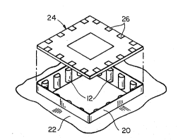
As mentioned above, Figure 2 illustrates the solder post
delivery system of Figure 1 placed in a fixture 22 and having
a chip carrier package 24 positioned with respect thereto
such that the connection pads 26 on the edges of the package
are in alignment with solder 12. It is within the scope of
the invention as illustratèd in Figure 2 to have backing
means 20 include an additional adhesive surface on the back
side thereof to secure the delivery system with respect to
the fixture 22. Figure 2 illustrates such a delivery system
wherein the longitudinal ends of the positioning means are
closed into a loop which is capable of being pressed
outwardly to conform to a geometric configuration and is
capable of being retained in the con~iguration by the
additional adhesive surface for the interconnection of the
solder posts.
Figure 3 illustrates yet another fixture having two
members 28 and 30 which are movable with respect to each
other on the inside of a delivery system. As seen in the
~igure, the closed loop of the delivery system shown
generally at 32 is dropped onto the members 28 and 30 which
are expanded and which bend the delivery system from the
generally circular cross-section to a generally rectangular
cross-section, i.e., a desired cross-section that is comple-
mentary to the substrates to be interconnected.
- 13 -
. .
- ~ .
.
'
L c93 ~
Figure 4 shows yet another one-piece fixture wherein a
loop of the delivery system is capable of being bent from a
generally circular cross-section to a generally rectangular
cross-section. It can be appreciated that various geometries
of delivery systems can be conEigured with fixtures like
those illustrated in Figures 2-4 or the like.
Figure 5 discloses a delivery system similar to that
disclosed in Figure 1 but wherein the positioning means 34 is
folded along a line 36 passing generally midway between the
tops 38 and the bottoms 40 of the openings 42 providing
unobstructed access to the solder posts 44. ~t is also
within the scope of the invention for positioning means 34 to
be folded in more than one location along the longitudinal
axis. Multiple folds de~ining a serpentine structure secure
the solder posts in a redundant manner. The positioning
means 34 may be pulled away from the soldered posts, each
fold pulling away from the columns. It is understood that
the width of the openings 42 is preferably slightly smaller
than the diameter of the solder post 44 so as to create an
interference fit to secure the solder post 44 within the
openings 42. ~he delivery system also includes an elongated
and flexible backing means 46 as in the earlier described
embodiments but wherein the backing means 46 extends beyond
at least one longitudinal periphery 48 of the positioning
means 34 to provide a surface for securing the positioning
~eans 34. It can be seen that the backing means 46 has an
adhesive surface which is exposed through the openings 42 and
which extends beyond the periphery 48 of the positioning
means to secure the positioning means 34 with respect to a
substrate (not shown) to be interconnected.
- 14 -
.., ~
. ~
Figure 5 also discloses that the positioning means 34
may be cut transversely, as shown generally at 48, to allow
the positioning means to be bent with respect to the
longitudinal axis of the positioning means.
Figure 6 discloses in a plan and partially schematic
view a continuous method of fabricating a variety of delivery
systems including those described ~earlier. Speci~ically,
there is illustrated a ribbon of tape 50 (preferably Kapton)
having windows 52 punched by punch 54 as the tape is moved in
the direction generally indicated at 56. Subsequent to the
punching operation, a 1exible backing means 58 having at
least one adhesive sur~aae is applied to the back side of the
tape 50 and simultaneously or subsequently solder posts 60
are placed within the openings 52. At a further point, the
composite tape is severed by cutting by means shown
symbolically at 62. It is understood that it is within the
scope of the invention to cut by various means such as laser,
heat, blade, etc. The result is the solder post delivery
system shown at 64. In the embodiment shown in Figure 6, the
backing means 58 is cut by a separate cutting means 66 which
allows the backing means to extend beyond the longitudinal
periphery of the positioning means on one side thereof much
like the embodiment shown in Figure 5. It is understood that
the width of the positioning means may be varied to extend
beyond the tops and bottoms of th~ solder posts 60 or as
shown in Figure 6 may be generally coincident with the tops
and the bottoms of the solder posts 60. It is also within
the scope of the invention to use a tape 50 which is slightly
heat-recoverable in the transverse direction but not in tha
longitudinal direction. Heating of the delivery system is
- 15 -
, ji',~,~, '
acccmplished by heating means 68 shown symbolically to be an
infrared heat source. The result is that the solder poqts as
shown at ~0' extend beyond the transverse periphery of the
positioning means 50' to facilitate engagement with
substrates to be interconnected.
Figure 7 discloses the solder post delivery system
embodiment typically fabricated by the process and apparatus
shown in Fiyure 6. In this embodiment the positioning means
50' positions the solder posts 60' and the flexible backing
means 58 having at least one adhesive surface is connected to
the positioning means 50' and to the solder posts 60'. The
backing means 58 extends beyond at least the one longitudinal
periphery of the positioning means as shown to provide a
surface for securing the positioning means 50~O
Figure 8 discloses yet another embodiment wherein the
positioning means 70 is folded along lines 72 and 74
coincident with the tops and the bottoms, respectively, of
the openings 76 to form a U-shaped cross-section haYing a top
flange 78 and a bottom flange 80 that extend transversely at
right angles to the longitudinal axis of the delivery system.
This figure also illustrates a cut 82 in the top flange 78,
it being understood that a similar cut exists in the bottom
flange 80 to allow the positioning means to be bent out of
the plane of the positioning means.
Figure 9 discloses a solder post delivery system
substantially identical to that illustrated in Figure 8 but
wherein at least one of ths flanges 78' is provided with at
least one notch 84, the adhesive surface 86 of the backing
means being exposed through the notch 84. In this embodiment
an optional cover means 88 may be provided in removable
contact with the exposed adhesive surface 86 to protect the
surface before installation of the system.
- 16 -
' ~ ' '
:
Figure 10 illustrates yet another embodiment
encompassing many of the features illustrated in Figures 7-9
but wherein the positioning means 90 is folded along line 92
coincidant with the tops of the openings to form an L-shaped
cross-section having a top flange 94 that extends
transversely at a general right angle to the longitudinal
axis, the backing means 96 conforming to the top flange 94 to
provide an adhesive surface capable of securing the
positioning means with respect to a substrate. In this
embodiment the solder posts 98 are secured against the inside
of the delivery system in openings shown in phantom. The
view illustrates the back of the backing means, it being
understood that the adhesive surface is on the inside of the
backing means ~6.
Figure 10 also illustrates a cut 100 which allows the
positioning means and corresponding backing means to be bent
out of the plane of the positioning means or at an angle to
the longitudinal axis o~ the delivery system. By
longitudinal axis it is understood that in the embodiments
shown in Figures 1-4 the delivery system and its components
comprise a single sheet of material which is readily flexible
along the longitudinal axis. However, the embodiments of
Figures 5-10 disclose delivery systems having bends which add
structural integrity along the longitudinal axes and are
therefore provided with cuts to allow the positioning means
and attached components to be bent out of the plane of the
positioning means along the longitudinal axis.
Figure 10 also illustrates a chip carrier package 102
having connection pads 104 to which the
3~ `
- 17 -
X
1 ~ 2 ~ ~ J~3 ~ .
-18-
aolder po~ts wlll beeome attached during installation
of the delivery system~ Thc figure illu~trateq that
the flange 9~ may be provided with a window opening,
the adhe~lve ~urface of the backing ~eans 96 bein~
exposed through the window openlng. An optional cover
mean3 106 ls in removabl~ contact with the exposed
adhe3ive surf`ace to protect the gurface before instal-
lation of the system, It i~ und~r~tood that window
ios ar~ the equivalent of tha notch 84 as sho~n in
Figure 9 and lq u~eful in all of the embodiments
whereln it i~ de~ired to have th~ pogl~ionlng means in
contact with a 3ub~trate and where it i~ de~irable to
have the adhesive gurface of the backing means avail-
able to secure th~ sy~tem wlth re~pect to a sub~trate.
Figure 11 illugtrateg yet another embodiment
wherein at least ~wo o~ tha opening~ 108 and llO
(shown in phantom) of the positioning means ll2 are
e~pty and the positioning means is folded tran~versely
wlth respect to said longitudinal axis between the t~o
openingsp the adheqive surface of the backing ~eans
ll4 extending through each of the two openings to
contact itself to deflne a tab and a corner for the
po~itlonin~ meana ll2 and for the delivery ~y~tem. As
sho~n in Fl~ura ll four opening~ at each corner are
empty and the positioning mean~ i~ folded midway
between the four opening~ to define a tab having two
open1ngs on each qide, a~ can be better 3een by
viewing opening~ ll6 and ll~ (~hown in phantom).
It should be appreciated that the u e of the
empty openings and interfacing o~ the backing mean~
allaw~ for a less severe bend to be placed in the
positioning means l12 on the interior of the deliver~
~ystem. SpecLfically, a3 seen in the figure, the
positioning means ll2, as noted generally at l20, is
-
..
'
'. ~
~2~
-19
bent at an angle of 45 from each interior ~urface to
fonm a total of a 90 bend in the positioning means.
Since the preferred material for the positioning means
i9 a Kapton tape which i~ relatively stiff, the 45
bend i~ easier to aocompligh than thc more severe
90. It is understood that at the far end 122 of the
tab, the po~itioning mean9 Ls bent a full 180 back
ont~ itself and may even be fractured. However, the
integrity of the tab is maintainQd by the matin6 of
the adhe ive surfaceg th~ough the openin~s as dis-
cus~ed earlier.
Figure~ 12-14 disclo~e yet another embodi-
ment of the instant invention wherein a solder post
delivery ~y~tem i3 provided having a positioning mean~
shown generally at 144 for pogitionins solder posts
146 wherein the positioning meang includes at least
three layer~ 148, 150 and 152. Each of the layer~ are
provided with a plurality of opening~ 154 there~
through, the openings in each layer being in generally
axial allgnment with the openings in the other layers,
the openings bein6 3l12htly ~isaligned (See Figure
13). The plurality of qolder po~t3 146' one solder
po~t being positloned in each generally aligned open-
ing are aecured therein by a force-fit created by the
sli~ht ml~alIgnment of the layer As ~een ~y the
arrows in Fl~ure 13, the misalignment i9 created by
movement of the layer with reqpect to each other.
~ Figure 14 iLlu~trate~ that the positioning
means 144 may be slit throu4h the Jeveral layer~ and
that the layer~ may be bent ~lightly out of plane of
the layer~ to define abuttment mean~ 156 for contact
and alignment of electrical component~ quch a~ the one
shown in phantom to be in:erconnecbed by the ~ystem.
.
.
,
~ ~ 2 C$ ~ ~ 3
Figure 15 illustrates yet another embodi~ent of the
instant invention wherein the positioning means 124 comprises
a continuous frame having an inner periphery 126 and an outer
periphery 128. The positioning means 124 is provided with
5 securing portions 130 which are capable o f removably
seauring solder posts 132 thereto when the frame is
continuous and which are capable of releasing the solder
posts that may be seaured thereto when the frame is
discontinuous as shown in phantom at 134. The plurality of
solder posts 132 in contact with securing portions 130 of the
positioning means are secured in the embodiment of Figure 15
by a force fit with openings in the positioning means 124.
Specifically, a frame of Figure 15 has a generally U-shaped
cross-section having top flange 136 and bottom flange 13~.
In this embodiment the securing portion on the inner
periphery of the frame comprises a plurality of spaced
openings 130 extending across the width of the inner
periphery 126 and into the top and the bottom flanges 136 and
138. Each of the solder posts 132 which can be more clearly
seen in the broken portion of the frame are held within one
of the openings 130 by contact with the edges of the opening.
The figure also illustrates that the frame may be cut as
shown generally at 140 so that the frame may be bent at the
corners thereof. At one corner 142 of the frame the
positioning means and backing means are discontinuous to form
a tab which may be separated after installation of the solder
post, the positioning means being separable from the solder
posts, again as shown in phantom.
The array of solder posts 132 are held in the fram~
which may be made of any temperature-resistant, non-
solderable material. The frame is formed as shown to have
- 20 -
.
, :. ~ :
: , ' . : ,
~ 3 22 ~ i .fJ
enough rigidity along each row to deliver the-solder post in
a straight line and the frame is made in a semi-continuous
strip making it convenient to snap in the solder posts. It
is folded at the predetermlned points to form the U-shaped
cross-section and extensions of the ~rame at the corner 142
are welded, glued or stapled.
Figure 16 illustrates another embodiment of the instant
invention wherein the positioning means 158 is made of a low-
durometer elastomer and includes a plurality of openings 160
therethrough to receive solder posts 162. Each of the
openings 160 is connected to the inner periphery of the
positioning means 158 by a slit 164, the slits 164 capable of
being widened to enlarge the openings 160 to release solder
posts secured therein when the frame is made discontinuous
15 such as by tearing the frame at cut 166. The openings 160
and slits 164 form a keyhole-type cut which allows the
positioning means to be simply pulled away from the solder
posts 162. Typical elastomers that may be utilized are
silicone rubber, Viton, (a trademark) polyurethane and
nitrile rubber. These types of low-durometer materials are
compliant enough that after the solder posts are reflowed at
the tops and the bottoms thereof the elastomeric positioning
means may be ripped off leaving the pins in place.
Figure 17 illustrates yet another embodiment of solder
post delivery system comprising an external, reusable, hinged
frame. Specifically, there is disclosed a positioning means
for positioning solder posts having a continuous, generally
rectangular frame 168, the frame capable of being
di~continuous at 170 upon removal of the pin 172, the
positioning means having securing portions 174 which are
capable of
- 21 -
r~ ~
, 1
.L ~ J U ;i
--22--
releasing solder posts 176 that may be secured thereto
when the frame is made discontinuous. In this embodi-
ment the inner periphery oE the frame 168 is contoured
to provide spaced securing portions 174 that are
complementary to some portion of the surface of the
solder po~ts to secure the solder pQst thereto. The
frame 168 is provided with corners, one of them being
discontinuous at 170 and including the separate remo-
vable fastening meaos in the form of the pin 172 to
hold the corner together. The other corners 178 are
bendable in a hinge-like fashion to open the frame with
respect to the solder posts -~o release the posts from
the securing portions. The solder posts 17S are held
in place against the spaced securin~ portions by the
use of a very small amount of glue or adhesive-type
material to temporarily hold the solder posts in
position.
Figure 18 illustrates another embodiment of
solder post delivery system having a positioning means
for positioning solder posts comprising a continuous,
generally rectangular frame 180, having an inner and
outer periphery, but wherein the frame remains con~
tinuous in overall configuration and is made from a
dielectric material. In this ~bodiment it is
understood that the frame 180 may be left in place
after the reflow of the solder posts 182. The solder
posts 182 are preferably a filled solder and the frame
180 is shaped and perforated to fit the individual
applicationO In this embodiment the securing portions
comprise openings 184 through the frame, the diameter
of the openings 184 being smaller in diameter as noted
at 186 than the general diameter of the solder posts
where the solder posts are secured within the openings
184. The figure also illustrates an alternate shape
,
;
,
'
: : '
~ 3 2 ~
-23-
of solder post 188 which extends generally from only
one side of the frame 180. Each type of solder post is
held in place by the offset of post material. The
posts are shown to be preferably somewhat tapered to
provide support. The dielectric material of the rame
180 may be any suitable dielectric material such as
mica or Kapton, etc.
Figure 19 illustrates a solder post delivery
system comprising a positioning means for positioning
solder posts comprising a continuous r generally rec-
tangular frame 190 and a plurality of solder posts 192.
The frame 190 is preferably continuous across the inner
periphery thereof and comprises a thin sheet of solder
from which the solder posts 192 extend generally normal
thereto. In this embodiment the frame 190 is capable
of being discontinuous upon heating the frame or thin
sheet of solder since the solder is capable of flowing
to supplement the solder posts 192. In this embodiment
the securing portion of the positioning means is the
integral connection of the solder posts I92 and the
sheet 190.
Also illustrated in Figure 19 is the die 194
shown in pbantom illustrating apparatus which is
capable of ~abricating the solder delivery system.
Specifically, it can be seen that a sheet of fuseable
material or solder may be placed in the lower part of
the die and hit with the upper part of the die
resulting in the formed solder posts 192 connected and
capable of being delivered by the remaining attached
flash forming the thin shee~ of solder for positioning
means 190. It is understood that that starting sheet
of material may include a thin copper mesh or other
filler that will give integrity to the construction but
which will disappear from the sheet 190 upon heating.
` : ~: :
,: ` ' '
~ 3 ~" ~ , ~
Figure 20 illustrates yet another embodiment of the
instan~ invention wherein the solder delivery system
comprises a positioning means 196 for positioning solder
posts, the positioning means having a plurality of openings
~98 therethrough and further including a plurality of solder
posts with one post per opening, the posts comprising solder
paste 200 which ~ills the openings 198 to define individual
solder posts. In this embodiment, the solder paste 120 is
extruded into the openings lg8 by wiping the ~older paste
across the surface of the positioning means lg6 by wiping
means 202.
Figure 21 illustrates an alternative approach to
fabrication of the delivery system wherein the positioning
means 204 and the solder paste 206 are co~extruded in one
direction to define a continuous composite, the composite
being sliced through at an angle perpendicular to the
direction of co-extrusion to define an individual solder
delivery system shown generally at 208. Solder paste used to
fabricate the embodiments of Figures 20 and 21 may be made
from a solder and spherical and/or angular wettable,
conductive, high melting ~iller particles forming a paste
having a percentage of solder filler, resin, flux and other
materials as desired. For all of the embodiments of the
instant invention suitable joint-~orming material in the form
of filled solder composition, paste or supported solder which
will retain its shape upon the solder melting and reflowing
arew within the scope of the instant invention. As used
herein by the term "filled solder" and solder paste are
discussed the commonly assigned published U.K. application
Ser. No. GB 2,142,568A.
- 24 -
,, ~ 4: ~
' ,',' ' , ':
' . ' ~' ' ~ ,
.
-25-
Figure 22 illustrates method and apparatus for
fabricating a preleaded chip carrier package 210, the
method comprising the steps of providing a reusable
solder post delivery system de~ined by a mold 212,
having a chip carrier package securing portion 21~ in
one side thereof, and having openings 216 therethrough
for solder posts extending from a securing portion 214 to
the other side of the mold Z12, as seen in Figure 22A;
inserting a chip carrier package 218 in the portion
214; inserting solder posts 220 through the openings 216
into contact with the cbip carrier package 218 (as can
be seen in Figure 22B wherein the mold 212 has been
turned over, as noted by the directional arrow);
clamping the solder posts 220 and the chip carrier
package with respect to the mold 212 (as can be seen in
Figure 22C) while reflowing the solder posts to secure
the solder posts 220 to the carrier package 218; and
finally removing the mold to produce the prele~ded chip
carrier package (as can be seen in Figure 22D). The
above apparatus may be made disposable by using --
dissolvable material such as water soluble aluminum for
mold 212. Aluminum rasists being soldered to and is
structurally reli.able for the intended application.
Figures 23 and 24 illustrate another embodi-
ment of a solder post delivery system of an heat-
activated mechanically removable positioning means for
solder posts. Specifically, there is disclosed a posi-
tioning means 222 for positioning solder posts 224, the
positioning means being generally planar and having a
plurality of openings 226 therethrough, the positioning
means being made from a heat-recoverable polymeric
material and the positioning means having a first
dimension, as ~een in
' ~: . :'
~: .
.
~ 9~ J' ~J
Figure 23, including a first thickness wherein the openings
have a first diameter and the positioning means having a
second dimension as seen in Figure 24, including a smaller,
second thickness and wherein the openings have a smaller
second diameter. The plurality of solder posts 224 with one
posts per opening are secured by a force fit within the
openings when the openings are at the smaller, second
diameter. It can be appreciated that when the openings are
at the first diameter the solder posts are released, the
positioning means being capable of going ~rom the second
dimension to the first dimension upon application of heat.
In the embodiment of Figures 23 and 24 a flat sheet of
radiation cross~linked polymer is punched in the desired
pattern and the opening diameter is larger than the column
diameter of the solder posts. The positioning means is then
pressed while above the melt point to decrease the opening
diameter while the opening spacing is maintained. The
positioning means is then cooled and the smaller opening
dimension is set temporarily. The solder posts are then
inserted as seen in Figure 24. During khe heating of the
system and the reflow of the solder, the positioning means
returns to its original shape and dimension as seen in Figure
23. It is then possible for the positioning means 222 to be
easily removed mechanically. Suitable heat recoverable
materials such as polyethylene, Kynar (a trademark) and other
materials are well known as well as the cross-linking
technology use~ul to elevate the melting point of the
polymeric materials above that of the fusible solder posts.
- 26 -
~; j
" ~,
. ~
.
~ 3 r, ~
Figure 25 illustrates an embodiment of the instant
invention in the form of a solder clip delivery system. In
this embodiment a sheet of flexible, non-solderable material,
such as plastic, is prepared to have flat, thin traces of
solderable metal such as copper deposited in given arrays on
one surface. Solder is then placed on the metal. The
ass~-mbly is formed to bend the metal into a shape so that the
solder coated surface faces outward so that portions of the
surface are parallel with each other. This assembly is
placed between a chip carrier package having matching
solderable pads and a corresponding substrate having like
pads. The application of heat flows the solder, causing the
permanent joint to be made between the chip carrier pads and
the substrate. The act of heating preferably loosens the
bond between the material under the metal and this material
may be pulled out and removed, if des~red, increasing the
durability of the joints and allowing them to flex more
freely. A similar structure may be fabricated by adhering a
thin metal layer over an insulated centerpiece and
subse~lently trimming the metal layer and center piece at the
edges thereof to create outwardly extending conductive items
which become clips. This structure will be discussed later
with respect to Figure 35.
Figure 25 is a perspective view of a complete device
shown generally at 228 wherein 230 is the positioning means
for positioning the solder clips and comprises a generally
rectangular frame having top surface 232 and bottom surface
234 and having an inner and outer periphery, the inner
periphery of the frame having portions having a solderable
metal deposited thereon and having solder plated on the metal
to
- 27 -
. . .
., :
~ ;, 2
-28-
define individual solder clips 236. The rectangular
frame may be cut as noted in phantom at 237 to remove
the frame as will become apparent from the Eollowing.
Figure 26 i~ a partial cross~sectional view of
a solder clip 236 shown in phantom. The figure
illustrates how the clip is formed wherein the posi-
tioning means 234 referred to as the frame has had
solderable metal 238 deposited thereon and has solder
240 plated on the metal to define the individual solder
clip .
Figure 27 shows a cross-section similar to
Figure 26 wherein a chip carrier package 242 is posi-
tioned above the solder clip delivexy system 228 which
is, in turn, positioned above the substrate pads 244.
Figure 28 illustrates the parts in position
a~ter the application of heat wherein the solder 240
flows and joins the metal 238 to the chip carrier 242
and the substrate pads 244. As mentioned earlier, the
delivery material referred to as the positioning means
234 may be pulled away from the metal strips and
discarded. Thus, it can be seen that the frame 34 is
capable of being detached from the clips when heat is
applied to the clips, the heat melting the solder to
cause a permanent joint between the metal and the com-
ponent to be connected in loosening the frame from
metal. It likewise can be seen that the inner
periphery of the frame, having the portions of
solderable metal deposited thereon project inwardly and
are fingerlike portions having the metal deposited on
the top surface thereof, the portions being bent out of
the plane of the surface to form a generally C-shaped
solder clip.
.
::
:. . :
: . .
~3(~ J
Figure 29 illustrates a method of fabrication wherein
the frame is defined by two parallel layers 246 and 248, each
layer having portions projecting from only two opposite sides
thereof and the layers being oriented at right angles to each
other so that the portions project inwardly from all sides of
the frame when the layers are brought together. In other
words, the two opposed rows of termination strips are
combined at 90 angles to each other and once formed into the
pxeferred C-shapes will have pads alosely adjoining in the
corners. Item 250, in Figure 29, and item 252, in Figure 25,
are optional plating busses for the attachment of a current
source to improve metal deposition as is known to one skilled --
in the art. Such an optional plating buss is removed a~ter
plating is accomplished. A conductive polymer may be used
instead of a plating buss 250 in Figure 29, 252 in Figure 25
and yet to be described 262 in Figure 30. The conductive
polymer frame members provide an integral current return path
~or the electro deposition of the metals to make the clips.
Figures 30 and 31 illustrate a variation in the solder
clip delivery system described above wherein the solderable.
metal 252, as seen in the cross-sectional view of Figure 31,
taken along section lines 31-31 of Figure 30, is deposited
along the inner periphery 254 and the top surface 256 and the
bottom surface 258 in a spaced-apart fashion, as seen in
Figure 30, to define C-shaped configurations upon which the
solder is plated to define individual solder clips 260. In
Figure 30, areas 262 are plating busses which may ba punched
out prior to the use of the device. In the embodiments of
Figures 30 and 31 everything is similar in arrangement in
function to the formed clips described with respect to
- 29 -
.. . .
~ 3 ~ '~J tJ .~
Figures 25- 29, except that the solder clad opposed C-shaped
solder clips are fa~ricated around the edge of positioning
means, the opposed sides and adjoining edges are sensitized
by chemical and other well known processes to form a site for
metal deposition. Doing so in a direct way allows for much
finer features to be created and it also permits the features
to be formed closer together. Figure 30 also illustrates how
nested rows of solder clips may be fabricated.
Figures 32-34 illustrate yet another chip carrier
joining device using solder-clad deposited metal over an
insulative supporting structure, several of which may be
arranged to form an array. In this embodiment, the
supporting structure may be removed by heat recovery from the
supporting structure or by chemical means. Removal of the
supporting means facilitates inspection and improved
flexibility of the joints. Specifically, there is disclosed
a solder ring delivery system shown generally at 264,
comprising a positioning means for positioning solder rings
266, the positioning means including a plurality of
diametrically heat-recoverable rods 268, the rods being
adjacent to each other in spaced parallel relationships. It
is also within the scope of the invention to use tubes and it
is understood that the term "rod" as used herein includes
tubing. The dalivery system includes a plurality of solder
rings 266 positioned about the rod, the rods having surface
portions about the rods, upon which a solderable metal has
been deposited and having solder plated on the metal, the
metal and the solder defining the individual solder rings
266. The rods 268 are preferably diametrically shrinkable
upon application of heat and are therefore capable of being
removed.
- 30 -
. -..
' ~
3 ( ~ J
-31-
The heat-shrinkable tube or rod may be plated
or clad with rings of similar coated metal. The rod
may al30 be chemically dissolvable. In either case,
the rod or tube is used to position the rings in place
between the chip carrier pads and the substrate pads.
~ter application of haat to join the pads to~ether by
means of soldering, as seen in Figure 34, the rods are
removed. Absence of the rods again permits joint
inspection. Absence of the supporting rod also permits
the rings to flex more freely, increasing the durabi-
lity of the joints during heat cycling and mechanical
flexing.
If a tube is used, it may be conventional
heat-shrinkable material which contracts radially
during application of heat. If a rod is used, it may
be foamed so that upon heating it collapses to a
smaller diameter. Ir the rod is chemically removed, it
is fabricated from a material which permits chemical
fabrication of the solder-clad rings.
The ringed rods can be fabrica~ed in a con-
tinuous process. The rod is photochemically (or the
like) sensitized to receive an electrolytic deposit of
metal. A plating buss wire 270 is pressed into contact
with the sensitized areas. Electrical plating then
builds the required metal thickness. Tin or other
suitable solderable metals are added in turn. The
plated buss wire is peeled off and discarded. The
electroplated tin and lead may be reflowed by select
infrared or radio-frequency methods so as not to shrink
the rod. Conductive polymer may be used ins~ead of
conventional material for the rod or tube to perform
tWO functions. In the first instance it may eliminate
the need for a buss wire 270 or the like during
plating. In the second instance, it may become
~ ~3~
hot enouqh to recover (shrink) if sufficient current is
applied.
Alternate ringed rods 26~ and unringed rods or
insulators 272 are grouped together in arrays to match given
pad-to-pad geometries. The group may be held together with
tape 274 or the like. After heating the tape 274 may be used
to remove all of the rods at once.
Figure 32 illustrates ring rods 268, separated by
unringed rods 272. Figure 33 illustrates the same
relationship for application of heat. Figure 34 illustrates
the array after application of heat and after the solder-
cladding 266a has joined opposing pads. The rods 268 and 272
have been reduced in diameter because of their plastic
memory.
lS Figure 35A referred to earlier shows a thin metal frame
276 having a square hole therethrough so as to overlap a
thin, insulative (non-metal, nonconductive, semi-rigid)
center piece 278. The two items are then adhered together
permanently to form a laminated structure.
Portions of frame 276 and center piece 278 are cut away
to produce a plurality of outwardly extending metal
projections 280 as seen in Figure 35B and may be further bent
into a "C" shape to interface and to be soldered to
conductive pads of a device to be connected Snot shown).
Partial cross-sectional view Figure 35C, taken alon~ section
lines C-C, illustrates the item 280. Partial cross-sectional
view Figure 35D, taken along secton lines D-D, illustrates
the finished "C" shape.
- 32 -
. ,,,j :,
: ~ .
.... -.
.