Note: Descriptions are shown in the official language in which they were submitted.
1322399
~AF~R CARRIER
BACKGROUND OF THE INVENTION
This invention relates to moldable plastic
wafer baskets or carriers for silicon wafers which are
designed for carrying and storing silicon wafers used in
the production of integrated circuit chips.
The processing of wafers requires that they be
successively immersed or sprayed with liquids and
gases. Some of the chemical baths include various
corrosive chemicals while certain of the baths are
extremely hot, in the range of 180C. Wafers that are
presently being processed have diameters as large as 8
inches. Typically, 25 of such wafers are within a
single wafer basket or carrier which requires that a
carrier be large enough for this capacity. Such a
carrier which is full of wafers will weigh eight to ten
pounds. Ten inch wafers are now starting to be used and
will be in common use in the foreseeable future.
Accordingly, the wafer carriers used to hold
the silicon wafers during processing are formed of
moldable plastic which preferably is inert and highly
resistent to the corrosive effect of chemicals used, and
highly resistive to the high bath temperatures regularly
employed during the processing. Conventionally, the
molded plastic used in carriers is PFA Teflon~ (a
registered trademark of E. I. du Pont de Nemours
Company), a perfluoroalkoxy-substituted
polytetrafluoroethylene resin. For less harsh
environments and for wafer storage and shipping,
carriers have been made of polypropylene.
- 2 ~ 1322 9 99
It should be recognized that the silicon wafers
are extremely delicate and brittle and may be only a few
thousandths of an inch thick. The silicon wafers are
extremely valuable and breakage of a wafer may represent
a significant loss. Particulate and other contamination
of wafers must also be avoided in order to manufacture
integrated circuit chips operable within the range of
standards set by the industry. Thus, there has been an
increase in automated handling away from manual handling
of the silicon wafers and carriers. Robotic arms are
increasingly being utilized for handling both the wafer
carrier and the individual silicon wafers where
possible.
Automated handling of silicon wafers and wafer
carriers require that the envelope of space within a
carrier wherein a particular silicon wafer is to be
located must be maintained within close tolerances.
This is necessary to avoid wafer breakage. Problems
have been encountered in handling these large but thin
silicon wafers because the wafer carriers have been
known to soften and distort when exposed to 180C.
temperatures. Also, warping of the wafer carriers
during their cooling down period after injection molding
has also been known to occur. Such warping, distorting
and bowing of the wafer carriers tends to put added
compressive pressure on the edges of the delicate
wafers. Therefore, a moldable plastic, distortion and
warp resistent wafer carrier is highly desirable for
processing, carrying and storing silicon wafers.
1322999
-- 3 --
A moldable plastic, distortion and warp resistant wafer
carrier is here described having an open top for insertion and
removal of wafers with opposed upright end walls. Side walls
with inner opposed ribs for spacing axially aligned wafers in
the carrier are provided wherein one upright end wall is
H-shaped with a horizontal indexing bar extending thereacross
intermediate the height of the carrier while the other upright
end wall is comprised of a center panel and two side panels each
oriented at an oblique angle relative to the center panel. The
center panel has a planar outer surface with an upriqht center
line and two planar inner surfaces being oriented obliquely to
each other at the center line so that the center panel is
thinner adjacent the center line than at outer edge portions of
the center panel. A transverse outwardly extending upper flange
is on each side wall. Each flange has at least two anti-warp
indentations adjacent its respective ends to permit the mold to
hold the wafer carrier in its originally molded shape as a wafer
carrier cools in the mold thereby minimizing the warp of the
wafer carrier within the mold.
A principal objective of this disclosure is to provide a
wafer carrier that remains in its original shape when formed
within the mold free of warpage as it cools during its
solidification.
Another object of this disclosure is to provide a wafer
carrier that is highly resistant to distortion and warpage when
exposed to extreme temperatures and caustic baths common to the
processing steps of silicon wafers.
`` 1322999
Another objective of this disclosure is to provide a wafer
carrier which will readily permit safe automated process
handling of the wafer carrier and silicon wafers therein by
robotic or mechanical arms without undue wafer breakage
specifically due to the minimal dimensional deviations of the
wafer carrier from the specified tolerances.
The embodiments of the invention will now be described
with reference to the accompanying drawings wherein:
BRIEF DESCRIPTION OF THE ~RAWINGS
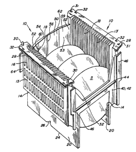
Fig. l is a perspective view of the wafer carrier
embodying the invention carrying silicon wafers;
Fig. 2 is a top view of the wafer carrier;
Fig. 3 is a rear elevational view of the wafer carrier;
Fig. 4 is a side elevational view of the wafer carrier;
Fig. 5 is a front elevational view of the wafer carrier;
and
Fig. 6 is a view of the wafer carrier taken along lines
6-6 of Fig. 2.
DETAILED SPECIFICATION OF THE PREFERRED EMBODIMENTS
Referring to Figs 1 - 6, the wafer carrier with silicon
wafers 5 embodying the present invention may be seen and is
generally referred to by reference numeral lO. Wafer carrier 10
is suitably injection molded integrally in one piece fashion
appropriately out of plastic as previously mentioned.
- 5 - 1322999
Wafer carrier 10 has an open top 11 and an open
bottom 12. Upright sidewalls 13, which are mirror
images of each other, each have opposing lower offset
inwardly wall portions 14 with windows, cutaways or wash
slots 16 throughout sidewalls 13 to cooperate with open
top 11 and open bottom 12 to improve the application,
disbursement, rinsing and other flow of liquids through
the wafer carrier 10 and over wafers 5. Wafers 5 are
held in place by opposing and inwardly projecting
ribs 18 which are aligned to permit wafers 5 to be
carried by wafer carrier 10 in axial alignment with
predetermined space between each wafer 5.
Tapered foot panels 20 are substantially
parallel with respect to each other being along and
below offset portions 14 of sidewalls 13. The top
surfaces 22 of the tapered foot panels 20 comprise the
wafer support surface 22. By this arrangement, there is
minimal contact with the peripheral edges of the
wafers 5. The bottom surface 24 of tapered foot
panels 20 has a centrally located locating notch 26
which permits indexing or properly aligning the wafer
carrier 10 on or in a particular piece of machinery.
The bottom surfaces 24 convergently taper upwardly from
both ends of the respective panels 20 towards the
locating notch 26. By this design, tapered foot panels
20 act as four independent feet.
Each upper sidewall 13 also has a transverse
outwardly extending upper flange 28. While one
flange 28 on one sidewall 13 has upwardly protruding
pins 30, the other flange 28 on other sidewall 13 has
slots or holes 31 for receiving pins 30. The pins 30
and holes 31 arrangement permit a dump-transfer of
wafers 5 into or from another wafer carrier 10 of
1322999
-- 6 --
similar size. Located distally or at the respective ends of
flange 28 are anti-warp indentations 32 which suitably may be
holes, notches or depressions which suitably permit gripping of
the wafer carrier 10 by the mold as the wafer carrier begins to
cool when the liquid plastic begins to solidify.
Wafer carrier 10 has an H-shaped end wall 40 with an
H-shaped flange 42 supporting a horizontal indexing bar 44
commonly used for indexing the wafer carrier 10 in or on a piece
of machinery. Robotic pickup flanges 46 are also provided at
the juncture of end wall 40 and side walls 13 to permit robotic
handling of wafer carrier 10.
Three panel end wall 50 opposes H-shaped end wall 40 and
consists of side panels 52 and central panel 54. Central panel
54 has an upright center line 56 along which is the thinnest
portion of end wall 50. Center panel 54 also has a planar outer
surface 58 with outer edge portions 59 adjacent side panels 52.
Center panel 54 also has a first planar inner surface 60 and a
second planar inner surface 62 oblique to each other and each
adjacent center line 56. End wall 50 also suitably may have
robotic pickup flanges 64 similar to robotic pickup flanges 46.
Remembering that the principal objects of this disclosure
are a moldable plastic, distortion and warp resistant wafer
carrier, the novel features may now be appreciated.
After the molten plastic has been completely injected
into the mold to cast the wafer carrier lO, the plastic
begins to change from liquid to solid. Firstly,
1322999
the molten plastic forms a skin while the inner portions
of the wafer carrier 10 are still molten. This chemical
change has been found to cause stress within molded
carriers. The thicker the particular section wafer
carrier is typically associated with greater internal
stresses at that location due to a longer setting up and
cooling period.
Consequently, as wafer carrier 10 begins to
solidify within its mold, stresses due to the chemical
change going from a molten state to a solid state may
act upon wafer carrier 10 in a manner that upper
sidewalls 13 and end walls 40 and 50 may begin to pull
away from the inner surface of the mold as the wafer
carrier 10 cools and solidifies in the mold.
If the mold has some protruding element such as
pins, in the area of upper flanges 28 to form and fit
anti-warp indentations or holes 32, the mold will
effectively hold the wafer carrier 10 in its original
position as it changes from a molten to a solid state
thereby minimizing the ch nce of warp and increasing the
possibilities that the wafer crrier 10 will remain in
its originally molded and specified condition.
It has generally been past practices to mold
wafer carriers out of plastic having a uniform wall
thickness. However, the thicker wall portions create
more internal stresses due to the required longer
cooling period to thereby permit the plastic to set up
from a molten to a solid state. Such carriers are more
susceptible to distortion, warpage and bowing.
Consequently, the thinning of the wall portions of end
wall 50 minimizes internal stresses which may later
. - 8 - 1322~99
cause the wafer carrier to distort or warp due to its
expected exposure to hot chemical baths.
Three panel end wall 50 has a varied thickness
with a thinning towards the center line 56.
Additionally, end wall 50 essentially has four inner
planar surfaces 53, 53 and 60, 62 of the respective side
panels 52 and center panel 54. This angularity alone
with respect to three panel end wall 50 further adds
rigidity, and warp and distortion resistance to wafer
carrier 10.
The present invention may be embodied in other
forms without departing from the spirit or essential
attributes thereof, therefore the illustrated
embodiments should be considered in all respects as
illustrative and not restrictive, reference being made
to the appended claims rather than to the foregoing
description to indicate the scope of the invention.