Note: Descriptions are shown in the official language in which they were submitted.
13230~4
BIO-PHOTOSENSOR
The present invention relates to a bio-photosensor
adapted to be fixed to a part of the body of an examinee
e.g. a finger to measure the absorption of the light
emitted from one side of the finger and transmitted through
the finger to the other side.
This type of sensor is used e.g. to examine the
function of the liver of an examinee. In this examination,
a specific pigment which is selectively taken into and
excreted from only the liver is injected into the blood
stream. Then the concentration of the pigment in blood
plasma is measured with the sensor to determine the blood
plasma disappearance rate and retention ratio of the
pigment to examine the function of the liver.
As one example of such prior art photosensors, there
is known a bio-photosensor which is applied to a finger
and in which light is transmitted from one side of the
finger to the other side so as to detect the fluctuation
of transmlttance or reflectance of light due to the blood
flow. Signals representative of such fluctuatLons are
processed and calculated to obtain such vital information
as pulse rates or blood pressures (see Japanese Unexamined
Patent Publication No. 60-34432 and Japanese Unexamined
Utility Model Publication No. 60-158803).
_
~ ~ .
~3230~4
Such a prior art photosensor is provided on its
base film with a light emitter capable of emitting two
beams having different wavelengths from each other.
But no photosensor is equipped with a light emitter capable
of emitting two beams, one of the beams having such a
wavelength as to be absorbed almost entirely by a specific
pigment which is removed exclusively by the hepatic
parenchyma once it is injected into the blood and the
other having such a wavelength as not to be absorbed
by the abovesaid pigment. Elaborate equipment was
therefore necessary to measure the absorption of a pigment
e.g. in the blood.
It is an object of the present invention to provide
a bio-photosensor which can be fitted on a part of the
body of an examinee easily and comfortably.
In accordance with the present invention, there
'is provided a bio-photosensor comprising a flexible printed
circuit board formed with an electric circuit- and adapted
tn be wrapped around a part of the body of an examinee,
and a light emitter and a light receptor mounted on the
printed circuit board with some distance therebetween
so that they will be opposed to each other at both sides
of the part of the examinee when the printed circuit
board is wrapped therearound, the light emitter and the
light receptor being electrically connect~d through the
electric circuit to an electric cable connected to one
end of the printed circuit board.
- 2 -
1323~74
The bio-photosensor preferably allows the light emitter and the
light receptor to be disposed in exactly opposite positions to
each other when the bio-photosensor is fitted on a finger or the
like. Accordingly, preferably there is provided a position
displacement detector means which has a pair of sensors in the
vicinity of the light receptor to check whether or not the light
receptor is exactly opposed to the light emitter.
As another means for this purpose, there is provided
a bio-photosensor having a strip of flexible printed circuit
board provided with a mark at a portion adapted to be brought
into contact with the tip of a fingernail.
Preferably the bio-photosensor is capable of emitting
a plurality of beams having different wavelengths from one
another, one of said beams having such a wavelength as to be
absorbed by a specific pigment which is removed exclusively by
the hepatic parenchyma when it is injected into the blood, and
the others having such wavelengths as not to be absorbed in this
pigment. In order to accomplish this, one light emitter may
comprise a light emitting diode emitting a beam of the first
wavelength and another light emitting diode emitting a beam of
the second wavelength.
- 3 -
.
,
132307~
Other features and objects of the present invention
will become apparent from the following description taken
with reference to the accompanying drawings, in which:
Fig. 1A is a plan view of a prior art bio-photosensor;
Fig. 1B is a front view of the same;
Fig. 1C is a sectional side view of the same fitted
on a finger;
Fig. 2A is a plan view of the first embodiment of
the photosensor according to the present invention;
Fig. 2B is a front view of the same;
Fig. 3 is a front view of a modification of the
first embodiment;
Fig. 4 is a plan view of the second embodiment;
Fig. S is a circuit diagram showing how the
photosensor of the second embodiment works;
Fig. 6A is a plan view of the third embodiment;
Fig. 6B is a front view of the same;
Fig. 7 is a side view of the same showing how it
is fitted on a finger;
Fig. 8A is a plan view of the fourth embodiment;
Fig. 8B is a front view of the same;
Fig. 8C is a side view of the same showing how it
is fitted on a finger;
Fig . 9A is a plan view of the fixing tape of the
photosensor of the fifth embodiment of the present
6~ ,
, - 4 -
-. ~
. :- - .. .:
. - : , . . :. . ~
.
- '- ~ ' ' : .; . ... ,: .
,
132307~
invention;
Fig. 9B is a front view of the same;
Fig. 10 is a plan view of the release paper of the
photosensor of the sixth embodiment;
Fig. 11 is a sectional view of the fifth embodiment
showing how it is fitted on a finger;
Fig. 12 is a plan view of the fixing tape of the
sixth embodiment with the release paper partially peeled
off;
Fig. 1 3A is a plan view of the multi-wavelength
light emitter used in the bio-photosensor of the seventh
embodiment with the cover removed;
Fig. 1 3B is a bottom view of the same;
Fig. 14 is a perspective view of the multi-wavelength
light emitter; ~
Fig. 15 is a block diagram of the same;
Fig. 16 is a plan view of the seventh embodiment
equipped with the multi-wavelength light emitter of Fig.
14t
Fig. 17A is a plan view of the eighth embodiment;
and
Fig. 17B is a front view of the same.
- 5 -
~i i! ;
.
1323û7~
Figs. 1A and 1B show a prior art bio-photosensor
comprising a strip of flexible base film 1, and a light
emitter 2 and a light receptor 3 mounted on the ~ase
film 1 and spaced longitudinally from each other. The
emitter 2 and the receptor 3 are connected respectively
to lead wires 4. An adhesive tape 5 is used to fix the
photosensor 6 to a finger.
The base film 1 provided with the emitter 2 and
the receptor 3 is applied to a finger 7 in its longitudinal
direction and turned back at the finger tip 7a. ~Fig.
1C) The tape 5 is then put over the base film 1 to fix
the photosensor 6 to the finger 7.
In this state, the sensor 6 is turned on to cause
the light emitter 2 to give forth light which passes
through the finger 7 and strikes the receptor 3. In
response thereto, the receptor 3 applies signals to a
signal processor (not shown) through the lead wire 4
and a connector (not shown). The processor will process
the signals about the fluctuation of light transmittance
to obtain vital information such as pulse rate and blood
pressure.
In this prior art photosensor, wires are directly
connected to the emitter and the receptor and they have
to be fixed to the flexible base film. Means and step
of fixing the wires to the base film will add to the
-- 6 --
,
~ :
: ~
.
1323~7~
cost of the photosensor.
Also, the rigidity of lead wires extending in the
longitudinal direction of the base film will lower the
flexibility of the base film. Such a photosensor could
not be comfortably fitted on part of the body of an
examinee. Further, there was a fear that the wire or
cable might be pulled out of the sensor or be broken
at their connections during use only with a small tensile
or bending stress which tends to act on the connections.
In Fig. 1C, the emitter 2 and the receptor 3 are
set in exactly opposite positions to each other. But
if they are not, it is necessary to increase the power
of the emitter 2 or the amplifying factor of the receptor
3. If the power of the emitter is increased, the finger
might be burned owing to a heat buildup of the emitter.
An increase in the amplifying factor of the receptor
would impair the S/N ratio, thus lowering the accuracy
of the photosensor. This problem results from the fact
that the photosensor is not equipped with means for
ensuring the relative position between the emitter 2
and the receptor 3 when the photosensor is fitted on
the finger.
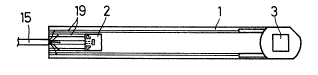
Figs. 2A and 2B show the first embodiment of the
present invention in which a flexible printed circuit
(hereinafter referred to as FPC) board 1 is etched on
~ 7 ~
.
:. - . , , :'' . . '
.
1323~7~
its one side with a required electrode pattern (conductor
circuit 19). A light emitter 2 and a light receptor
3 are mounted on the FPC board 1 in position and connected
to the conductor circuit 19 by soldering. A cable 15
is also connected at one end of the FPC board to the
conductor circuit 19 by soldering.
The light emitter 2 is a several-millimeter square
chip having two light emitting diodes mounted thexeon.
The lights emitted from the two diodes have different
wavelengths from each other. The transmittance of one
of the lights through the body of an examinee is used
as a reference on the basis of which the transmittance
of the other is measured. Two diodes are used for precise
measurement.
As the light receptor 3, a silicon photodiode is
used. The cable 15 is a five-core cable, three of the
five cores for activating the emitter 2 and the other
two for relaying the signals from the receptor 3.
The photosensor in the first embodiment should
preferably be provided with protective layers 16 and
17 as shown in Fig. 3. The layer 16 covering the light
emitter 2 and the light receptor 3 is made of a transparent
resin or glass. The layer 17 covering the other part
of the photosensor is made of an insulating and flexible
resin such as epoxy, urethane or silicone resin.
-- 8 --
~ . .. . .
: , ., , .: ~
.
~: , , : ~. .. :. . :
- :- : .. .:. .: .
- . :- ~:
:: : ,::
. ;, ~ .
, . . . .
~32~Q74
The photosensor in this embodiment is applied e.g.
to a finger so as to sandwich the finger with the emitter
2 and the receptor 3 opposed to each other at both sides
of the finger and fixed in position by means of a fixing
tape. The light emitter 2 is then activated to emit
two beams of light having different waveLengths from
each other. The beams are transmitted through the finger
to hit upon the receptor 3. The light beams received
on the receptor are analyzed to determine the content
of pigment in the blood stream, etc.
In this embodiment, the FPC board is used as supports
for the light emitter and the light receptor and they
are connected to the cable through the conductor circuit
on the FPC board. It is not necessary to mount the cable
on FPC so as to extend in its longitudinal direction.
It is thus not necessary to apply a tape for fixing the
cable to the FPC board, either. The photosensor in this
embodiment is more flexible and can be fitted more
comfortably on a finger or the like. Further, its
reliability is increased and the production cost is
reduced.
Fig. 4 shows the second embodiment of the present
invention in which four position sensors A1 to A4 are
provided around the light receptor 3 to judge whether
or not the receptor is in an exactly opposite position
.~ . , ,, : ., ~
.
~' ' ' ' .
': . : ':', ' ' ' ~
.: , . ' , . . '
.
. ~ . , '' `
' , : ' '
13230~4
to the light emitter 2. The sensors A1 and A2 are arranged
in front and rear of the receptor 3 to determine whether
they are in exactly opposite position in the longitudinal
direction of finger and the sensor A3 and A4 are arranged
at ~oth sides of the receptor 3 tn determine whether
they are in an exactly opposite position in the transverse
direction of the finger. The light emitting diodes 2a
and 2b, the receptor 3 and the four position sensors
A1 to A4 are connected to a main body 20 through lead
wires 15 and a connector 10.
Fig. 5 is a circuit diagram showing how the
photosensor of the second em~odiment operates. An electric
current IA1 which flows through the sensor A1 and a current
IA1 which flows through the sensor A2 are compared with
each other in an IC comparator 30 to check the position
of the receptor 3 in a widthwise direction of the finger.
The result is expressed as IS1. Currents IA3 and IA4
which flow through the sensors A3 and A4, respectively,
are compared in an IC comparator 40 to check the position
of the receptor 3 in a longitudinal direction of the
finger. The result is expressed as IS2. The receptor
3 gives an output IB representative of the light
tranmittance. The position sensors and comparator means
such as IC comparators constitute a position displacement
detecting means.
- 10 -
, - . . .
: : ' '
.
.
132307~
If the emitter and the receptor are out of mutually
opposite positions, the relationship between the currents
IS1 and IS2 will be expressed by the inequality
¦IS1l ~ ISO ¦IS2¦ _ ISo, wherein ISo represents a preset
current. In such a case, an alarm may be set off to
give a warning to an operator so that he can refit the
photosensor to correct the relative position between
the emitter and the receptor.
Though in this embodiment, two pairs of position
sensors are used, they may be provided in any number
of pairs. For example, even one pair would be of a great
help in checking the relative position between the emitter
and the receptor.
Also, the number of light emitting diodes provided
in the emitter is not limited to two but may be one or
three or more.
Any positional displacement between the emitter
and the receptor is detected by comparing the electric
sianals from the position sensors. If any displacement
is detected, an operator is notified immediately so that
he can refit the photosensor so as to arrange the emitter
and receptor in exactly opposite positions. Since the
emitter and receptor can be positioned exactly in a
face-to-face relationship, it is not necessary to increase
the power of the emitter to such an extent as to give
1 1 _
.
.
.
1~2307~
a burn on the finger. Nor is it necessary to amplify
the sensitivity of the receptor which would lower the
S/N ratio and thus the precision of the sensor. This
will increase the reliability of the bio-photosensor.
The third embodiment is shown in Figs. 6A, 6B and
7. This embodiment is substantially the same as the
first embodiment except for the following points.
As shown in Figs. 6A and 6B, the photosensor is
provided with a mark 8 at a position where the tip of
the nail of a finger contacts when the photosensor is
put cn the finger. The mark 8 may be in the form of
a projection or a mere flat sign.
Next, it will be described how the bio-photosensor
in this embodiment is put on a finger with reference
to Fig. 7. The photosensor 6 is applied to a finger
7 so as to extend in its longitudinal direction with
the mark 8 in contact with the tip of the fingernail
7a. The photosensor is turned back at the tip of the
fingernail. The mark 8 should be provided on the FPC
board at such a position that the emitter 2 and the
receptor 3 will be put in exactly opposite position to
each other when the photosensor 6 is fitted on the finger
in the above-described manner.
Figs. 8A to 8C show the fourth embodiment of the
present invention which is a modification of the third
, , ~,
132'~074
embodiment. The mark 8 in the third embodiment serves
as a mere standard for the relative position between
the emitter and the receptor because the shape and length
of the nail and finger differ from person to person.
In this embodiment, besides the mark 8, second marks
9a and 9b are provided on the fixing tape 5 on its back
side so as to be located right behind the emitter 2 and
the receptor 3, respectively. They may be projections
or mere flat marks.
Next, it will be described how the photosensor of
the fourth embodiment is applied to a finger with reference
to Fig. 8C. After bringing the mark 8 into contact with
the tip of the fingernail 7a as in the third embodiment,
the photosensor 6 is turned back so as to wrap the finger
7 in its longitudinal direction. The emitter 2 and the
receptor 3 can be put in exactly opposite positions to
each other by aligning the mark 9a located right behind
the emitter 2 with the mark 9b located right behind the
receptor 3. Then the photosensor is fixed in position.
The second marks 9a and 9b will thus allow the emitter
and the receptor to be put in right positions irrespective
of the length of the nail and the shape of the finger.
Figs. 9A and 9B show the fixing tape used in the
fifth embodiment of the present invention. The fixing
tape 5 comprises a substrate 101, an adhesive layer 102
- 13 -
, . .
,:
13230~
bonded to one side of the substrate 101, a release paper
103 laminated on the adhesive layer 102. The release
paper 103 has a ~ab portion 104 and is formed with cutouts
105 at both sides so as to be opposed to each other.
The cutouts 105 are used as a positioning mark when
applying the photosensor to a finger of an examinee.
NameLy, the emitter and the receptor are mounted on the
finger so as to oppose to each other when the photosensor
is put on the finger with its cutouts 105 at the tip
of the finger, as shown in Fig 11. But, it is required
that the emitter and the receptor are exac~ly positioned
with respect to the substrate 101. For this purpose,
the substrate 101 is provided on its surface behind the
emitter and the receptor with a printed mar~ 106 so as
to indicate the positions of the emitter and the receptor.
The cutouts 105 serve also to form voids 105a and
105b as shown in Fig. 9A. If no voids 105a and 105b
are formed, these portions may stick together when the
substrate 101 is put on the finger, thus pressing the
finger so tightly as to cause it to be congested with
blood~
Fig. 10 shows the sixth embodiment in which the
release paper 103 in the fifth embodiment is modified.
Namely, it is formed with a perforated weak line 107
which outlines a portion on which the emitter and the
- 14 -
~, -
1323~
receptor are to be mounted. The perforated line 107
may be replaced with a half-cut line or a continuous
through-cut line. A tab 108 is provided at one end of
the portion enclosed in the perforated line 107O Another
tab 109 is provided at a desired portion along the edge
of the release paper 103 and outside the portion enclosed
in the line 107. Further, on the release paper 103,
there are printed letters 110 which indicate the posi~ions
o~ the emitter and the receptor and a mar~ 111 which
indicates the mounting position of a part (a finger in
the drawing) of the body of the examinee. The same mark
111 should be printed on one side of the substrate 101,
too, at a position corresponding to the mark on the release
paper 103.
In use, the release paper 1~3 is peeled firstly
only at the portion e~closed in the weak line 107 to
expose a part of the adhesive layer 102 as shown in Fig.
12. Then the emitter and the receptor are stuck in
position on the exposed part of the adhesive layer 103.
Next, the remainder of the release paper is peeled off.
Thus, the emitter and the receptor can be mounted in
exact positions easily. Since the adhesive layer 102
is covered with the release paper 103 except the portion
enclosed in the weak line 107, until right before the
tape is applied to the finger, its bonding strength is
- 15 -
l323a7~
kept high.
Figs. 13A, 13B, and 14 show an example of the light
emitter used in the present invention. A multi-wavelength
light emitter 210 (Fig. 14) includes a glass-epo~y board
201 having its entire surface except the el~ctrodes
subjected to etching. Light emitt~ng diodes 202 and
203 having different wavelengths are connected to a common
cathode 204 and to anodes 205 and 206, respectively.
The light emitting diodes 202 and 203 are mounted on
the circuit board 201 by wire bonding or die bonding.
On the other side of the circuit,board 2G1, electrodes
204', 205' and 206' are provided which correspond to
the electrodes 204, 205, and 206, respectively. Eac~
pair of the electrodes 204 and 204', 205 and 205' and
206 and 206' are electrically connected together through
a hole 207. The eLectrodes 204', 205' and 206' on the
other side of the circuit board 201 a,^e connected to
lead wires or directly connected to another circuit board.
As shown in Fig. 14, the light emitting diodes 202
and 203 mounted on the epoxy-glass board 201 are covered
with a clear epoxy resin 208. Three lead wires 209 come
from the back of the board 201. The board 201 may be
a 3 mm by 3 mm square with a height of 2 mm, for example.
The light emitting diodes 202 a~d 203 emit beams
A1 having a wavelength of 805 nm and beams A2 having
- 16 -
.
. :,
, ~
:,
~ ,
13230~4
a wavelength of 940 nm, respectively. (Fig. 15).
Fig. 16 shows the seventh embodiment i~ which the
multi-wavelength light emitter 210 and the light receptor
3 are mounted on the FPC board 1 formed with a printed
wiring pattern 212. The lead wires 209 and the wiring
pattern 212 are connected to the cable 15. In this
embodiment, the FPC board 1 is coated with an insulating
urethane resin.
In use, the FPC board 1 is put on the finger tip
7 in the manner as shown in Fig. 11 so that the light
emitter 210 and the receptor 3 will oppose to each other
at both sides of the finger tip 7.
Since the light emitter of the photosensor in this
embodiment is of a compact one-chip type, the photosensor
can be fitted easily on the finger tip or the like to
measure e.g. the concentration of a specific pigment
injected into the body of the examinee. Further, since
the two light emitting diodes are arranged very close
to each other, the beams emitted therefrom and having
different wavelengths from each other ean be regarded
as originated from a single light source. This will
simplify the signal processing.
Figs. 17A and 17B show the eighth embodiment which
is a modification of the seventh embodiment. ~s shown
in Fig. 17A, the FPC board 1 is integrally formed at
- 17 -
:'' '. :'
~323Q7~
its one end with a narrow strip 26. One end of the cable
is put on the strip 26 and bonded thereto. A heat-
shrinkable tube 27 is put on the overlapped portion and
heated so as to be shrun~ on the overlapped portion.
The photosensor as welL as part of the heat-shrinkable
tube 27 may be coated with a flexible resin to protect
the entire photosensor especially its connections to
wires. Such a coating has to be transparent at portions
covering the beam emitting and receiving faces of the
emitter and the receptor. If this coating is applied
to a stick-on type sensor other than a photosensor, it
may or may not be transparent.
In this embodiment, the cable has its one end
overlapped with and bonded to the narrow strip of
projection of the circuit board. Further, the heat-
shrinkable tube is put on the overlapped portion and
tightened to reinforce the bonding connection therebetween.
The cable is thus less likely to get disconnected or
broken. This will allow the base for the sensor elements
to be made of FPC. The photosensor having an FPC base
is superior in flexibility, easy to manufacture and can
be fitted aasily and comfortably. Still, its reliability
is sufficiently high.
18 -