Note: Descriptions are shown in the official language in which they were submitted.
. 7357
1323~ ~
TITLE: PROCESS FOR TAPERING WAVEGUIDES
Field of the Invention
This invention relates to channel waveguides
useful at optical wavelengths.
Background of the Invention
In optical waveguide systems, there is a need
for a coupling channel waveguide whose width
continuously varies from one dimension to another over a
relatively short length of the waveguide. This need may
arise, for example, when the waveguide is~used to couple
a single mode optical fiber whose core has one dimension
to an optical waveguide whose channel width has a
different dimension. -To couple efficiently, the
waveguide used for coupling should be relatively
lossless and remain a single mode waveguide despite the
change in its channel width be~tween the two dimensions
The latter consideration requires that the index of
refraction along ~he channel vary inversely with the
change in its geometry. These factors pose problems.
In particular, if the desired change in
channel width is achieved simply by forming, by the
normal photolithographic techniques, a channel whose
width tapers gradually between the two dimensions
needed, the;index of refraction of the channel guide
tends to remain uni~orm along the~length of the tapered
region because the concentration of the impurity added
to form the index of refraction change in the channel
'', ~ ' ~
.
~323~9~
tends to be uniform along such length. As a
consequence, because the width of the channel varies
along such len~th while the index of refraction remains
uniform along the length, the modal properties along the
region of taper vary. What is needed to maintain the
modal properties essentially constant along the length
where the channel width varies is a compensating change
in the index of refraction along such length.
The problem is especially critical with
waveguides that use a large index of refraction change
between the channel and its substrate to achieve tight
confinement of energy in the channel. The large index
change results in a large modal mismatch between the
relatively narrow single mode channel waveguides useful
in integrated circuit devices and the typically wider
optical fibers that are often coupled to such channel
waveguides.
Summary of the Invention
The present invention is directed to a process
for forming a channel ~aveguide whose wid~th and depth
can be varied in any desired manner along its length,
typically to taper in continuous fashion from a
relatively wide dimension to a relatively narrow
dimension over a short length, and in which the index of
refraction in the channel along such length varies in a
manner to compensate for the change in geometry. As a
result, the modal properties of the channel remain
essentially uniform over the length and a single mode
signal applied as an input at one end of the tapered
channel length can pass through to the other end with
little mode conversion and insignificant loss.
In this process, there is first prepared, by
any one of the known techniques, a waveguide channel of
uniform width and uniform concentration of the dopant or
impurity used to effect the index of refraction change.
The uniform ~width advantageously is chosen to match the
narrower of the dimensions lnvolved. Then the por:ion
.
.
.
.
~23194 63356-1701
of the channel whose width and depth is -to be changed is subjec-
ted to non-uniform heating along its length for a time and at a
temperature such that there is effected along such length a
prescribed non-uniform diffusion of the dopant or impurity. The
heating tends to diffuse the impurity outwards from the channel
at a rate determined by the temperature to increase its width
and depth. The non-uniform heating is chosen to unalter the
width of the channel at one end of the coupling region while
widening it at the other end. Moreover, because the same amount
of dopant or impurity will merely have been spread over a wider
waveguide volume, the increase in volume will have been compen-
sated for by a corresponding decrease in the index of refraction.
Various ways are feasible for providing the desired non-uniform
heating. In a preferred embodiment, successive limited portions
of the channel region involved are irradiated with localized laser
pulses, the number of pulses and/or the intensity of pulses
applied to successive portions varying from one end of the region
to the other end to provide a continuous change in width and depth
of the channel. This technique is attractive because of the high
degree of control possible, which permits reshaping the original
channel both widthwise and depthwise.
The invention may be summarized as a process for
making a waveguide whose cross-section changes along its length to
enhance coupling, said process comprising the steps of: initially
forming an elongated channel waveguide having exposed ends
structured for coupling, said elongated channel waveguide being
13231~4 63356-l70l
formed in a substrate and provided with a predetermined length-
wise cross-sectional geometry having a predetermined widkh by
selectively doping the substrate with ions of a species that
raises the index of refraction of the substrate, the concentration
of said index raising species of ions and the width o~ said cross-
section both being constant over the length of the waveguide; and
selectively applying heat along said elongated channel waveguide
to change its cross-sectional geometry and dopant per unit volume
concentration of said index raising ion species as a function of
length along a selected length of said waveguide by further
diffusing said index raising ion species widthwise and depthwise
in said substrate while retaining the initial cross-section and
concentration along the re~laining length of the waveguide the
lengthwise distribution of said applied heat being such that the
product of the concentration of said index raising ion species
taken as dopant per unit volume of substrate and the width of said
waveguide at any lengthwise section of the waveguide remains
constant along the length of the waveguide so that the modal con-
tent of said waveguide remains unchanged throughout the length of
said waveguide while its cross-sectional geometry changes from
one end thereof to the other so that said waveguide ends can be
coupled with external devices of matching geometry and modal
content; the selectively applying step providing a taper in said
channel waveguide.
Detailed Description of the Drawings
The invention will be better understood from the
- 3a -
~ .
, ' . ~ ':
' . ', ' ' ' ' ' ' .
.' ~ :
. ~ .. . . . . . . . . . .
: . . . .
.
t 3 2 3 1 9 ~ 63356-1701
following more detailed description taken with the accompanying
drawings in which:
Figure l shows schematically in perspective form
laser apparatus for heating a channel waveguide non-uniformly
in accordance with one embodiment of the invention;
Figure 2 shows the channel waveguide after being
treated in the apparatus of Figure :L; and
Figure 3 shows alternative apparatus for heating
- 3b -
. ' .
- ,
~32319~
a channel waveguide non-uniformly in accordance with
another embodiment of the invention.
Detailed Des_r ~t on of the Invention
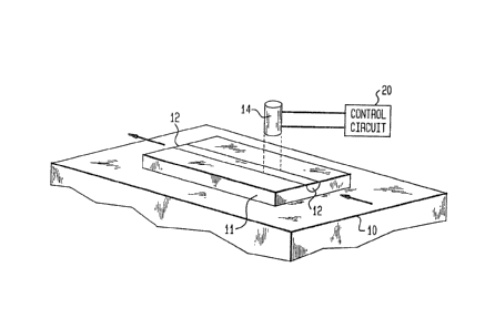
Referring now to FIG. 1, there is shown
schematically a platform 10 which can be stepped a
prescribed distance at a time in the direction indicated
by the arrows and at a rate determined by a suitable
control system (not shown) in the manner familiar to
workers in the art of processing microelectronic
devices. The control system permits the platform to
dwell at each position a prescribed period of time that
may be different at different positions. Typically, the
desired dwell time at each position is stored in a
program supplied to the control system before the
process is begun so that it can proceed automatically.
Positioned on the platform to move with it is
the workpiece, substrate 11 within which has previously
been formed a channel waveguide 12 in any of the ways
known for ~orming an optical channel waveguide. For
example, the channel waveguide may have been formed by
an ion exchange process in a silicate glass substrate
such as soda lime. This would typically have been done
after suitable masking to cover all its surface except
the elongated narrow portion in which the channel is
formed. Afterwards, the substrate is immersed for a
suitable time, for example about 52 minutes, in molten
silver nitrate at about 270C to exchange sodium in the
soda-lime glass for silver in the bath. Consequently,
there is formed along the exposed portion of the
substrate a narrow elongated channel that is doped with
silver. The silver doping increases the index of
refraction in the channel seIectively above that of the
undoped glass, whereby the channel serves as an optical
waveguide. This process tends to result in an index of
refraction change which is gradual. For a step index of
refraction change, it is feasible to use an electric
field-assisted ion exchange process in which the glass
-4-
: . - : . . ,
. . ' ' ' '. . ~ ~
.
~231~
substrate is dipped in a silver nitrate electrolyte
while the bottom surface of the glass substrate is
covered with a metal electrode maintained at a negative
potential with respect to the electrolyte. This process
can be carried out at lower temperatures than the first
described ion exchange process so that thermal diffusion
effects are reduced and a sharper almost step gradient
can be achieved in the silver concentration profile in
the formed channel.
It is of course feasible to substitute for
ions other than sodium in the glass and/or to use
dopants other than silver for the substitution to form
the waveguide, as is known to workers in the art.
Alternatively, the waveguide 12 could have
been formed in a ferroelectric substrate such as lithium
niobate using a proton exchange process.
A laser 14 coupled to a control circuit 20 is
positioned over the platform such that successive
portions of the channel 12 in substrate 11 pass under
the laser so that the laser output beam is incident at a
given time on a limited region of the cha~nel. There is
chosan for use a laser whose output wavelength and beam
size is appropriate to the channel being heated. In
particular, one choses a laser whose output wavelength
is within tbe absorption band of the substrate. Optics
may be included (not shown) to focus the output beam of
the laser on the channel. The laser may be operated
either in a continuous wave mode or in a pulsed mode.
Accordingly, by appropriately programming the stepping
of the platform, any desired dwell time of the laser
beam on a particular portion of the channel may be
obtained. In accordance with the invention, a desired
taper in the width of the channel is achieved by
appropriate variable heating of the channel by the laser
beam. Typical applications would be to widen a channel
region about two microns wide at one end to between five
and six microns wide at the other end over a distance of
--5--
.
.
1~23 ~9~
between one and ten millimeters. It is usually
desirable to keep the length of the taper short in the
interest of compactness. However, too abrupt a change
in width may lead to a waveguide which is extra lossy,
especially to desirable single mode transmission
therethrough. An advantageous rate of change in the
width would be one which satisfies the criteria for an
adiabatic change that are set forth in a paper entitled,
"Dielectric Tapers with Curved Axis and No Loss" by E.
A. J. Marcatili. IEEE Journal of Quantum Electronics
VQE-21, 307 ~1985).
It is a consequence of the thermal di~fusion
process involved in the heating technique described that
as the outward diffusion of the dopant widens the
channel, the concentration of the dopant in the widened
channel is decreased, since effectively the same number
of dopant ions are spread over a larger volume. It is
known that the modal content of a channel waveguide is
related to the product of the width of the channel and
the index of refraction change, and that the latter is
proportional to the dopant concentration in the channel.
Accordingly, if the width of the channel is increased by
the thermal diffusion but its dopant concentration is
reduced by the same ratio, the modal content of the
channel waveguide remains essentially unchanged.
Moreover, it is characteristic of the laser
heating technique described that the heating can be
largely localized near the top surface of the glass
substrate whereby the desired widening and deepening of
the channel can be achieved.
In FIG. 2, there is shown a typical result of
the treatment described with reference to FIG. 1. The
channel 12 in the glass substrate 10 has been modified
to include the tapered region 12A which widens from its
original width of typically 2 microns to an enlarged
width typically 4.7 microns, over a length of about 5
millimeters. The original guide which acts as a single
--6--
~32~ 94
63356-1701
mode guide a-t a ~avelength of .8 microns remains a single mode
guide despi~e the change in channel width.
There are of course various other forms o~ non~uniform
heating that can be used instead of that already described. For
example, the arrangement shown in F:[G. 1 could be modified to vary
appropriately the intensity o~ the :Laser or the focus or spot size
of the laser beam as successive por~ions of the channel moved
past, either at a uniform rate or a non-uniform rate.
Alternatively, the localized heating could be provided
by a heated filament, instead of a laser, past which was moved the
channel.
Still another possible technique is depicted
schematically in FIG. 3 ~n which a glass substrate 30, includiny a
channel 32, is mounted to keep one end in a fixture that includes
a support 33 maintained at one temperature for keeping that end of
the glass substrate essentially at that temperature. Typically,
the end of the substrate would be clamped to the support for a low
thermal resistance connection. The other end of the glass
substrate 30 is positioned in a hotter zone depicted by the
heating coil 34r to which is supplied heating current from the
current source 36. By keeping the two ends of the glass substrate
at different temperatures, a desired monotonic temperature
gradient can be established along the substrate to cause different
widths of ou~ diffusion of the dopant along the channel to achieve
the desired taper in the channel width. The spacing between turns
of the heating coil can be varied to help achieve a desired
temperature profile along the channel even in the heating zone.
Typically, the cold end may be kept at about 200C and the hot end
kept at about 300C. A time of between fifteen and thirty minutes
30 has been used to provide a widening of between two and four times
of the hot end of the channel. This technique will tend also to
result in a commensurate increase in the channel depth at the hot
- ', ' ~ '
,
~':
'
132319~
end. As previously mentioned, it is usually desirable
to maintain the temperature at the cold end sufficiently
low that little diffusion occurs at such end.
I t should be appaxent at this point that
various other techniques are feasible ~or perfor~ing the
desired non-uniform heating. These include pulling a
narrow heating element along at a varying rate to keep
successive portions of the substrate in the heating ~one
gradually shorter or gradually longer times.
Moreover, it should be apparent that the
principles of the invention can be used with a variety
of substrates so long as the dopant used to form the
waveguide diffuses appropriately in the substrate at
temperatures convenient to use and tolerable by ~he
su~strate.
In particular, the invention is similarly
applicable to channel waveguides formed in crystals,
such as lithium niobate or lithium tantalate, in which
the channel is formed by proton exchange to be quite
narrow for tight confinement of the optical energy.
Moreover, in some instances, it may be
advantageous to include a number of parallel channel
waveguides in a common substrate and to widen portions
of each of the channels in a common non-uniform heating
procedure of the kind described.
Additionally, it should be apparent that the
localized controlled diffusion technique, for example,
as described in connection with FIG. 1, can be used
~irst to widen a channel and then to taper the widened
channel back to the normal width so that any desired
variation with length along the channel above the
original width can be achieved.
Moreover, even though the inventive prccess is
particularly suitable for use in making tapered
structuxes for coupling single mode waveguides while
preseving their single mode nature, it should be
apparent that it also can be used for other applications
--8-- ~
1323194
where tapered waveguides would be useful such as for
coupling multimode guides to reduce insensi.tivity to
tolerance variations.
: : :
: ` _9~
: ~ :
- .
.
.