Note: Descriptions are shown in the official language in which they were submitted.
1 3234 1 6
The present invention relates to an RF switch.
More specifically, the present invention relates to an RF
switch for switching over an antenna input of a TV
receiver when the TV receiver, which is normally employed
for receiving a TV signal from an antenna, is instead used
as a monitor for a picture processing system, for example,
such as a personal computer, a video game system or the
like.
A video ~ame system and a personal computer, for
example, such as "ATARI 2600" (trade mark) and "COLECO
VISION" ~trade mark) which utilize a domestic TV receiver
as a monitor are well known. In such video game and
computer systems and the like, the TV signal input fro~ a
TV antennQ or a VTR must be switched over to an RF signal
(a TV signal) for the game or computer system. The
switchover is necessary to avoid interference between the
TV signals from the antenna and for the monitor as well as
from spurious radiation of the monitor's RF signal.
Accordingly, in the past, one of the two TV
signals has been selectively connected to the TV receiver,
in general, by a mechanical switch, for example, a slide
switoh. Typically, the slide switch is connected to hang
loosely in the vicinity of an antenna terminal of the TV
receiver. When using, for example, the game system, the
slide switch must be switched over by reaching, sometimes
only by feel, around to the back side of the TV receiver
to manually operate the switch. This operation is not
only troublesome but also dangerous because of the high
voltage equipment on the back side of the TV receiver.
~ principal object of the present invention i5,
therefore, to provide an RF switch whiGh is capable of
automatically switching a TV receiver from an antenna to
another video signal source, such as a picture processing
system, when the TV receiver is used as a monitor.
The present invention provides an RF switch
comprising a first input end for receiving a first TV
signal, an output end, a filter means connected between
the first input end, and the output end, the filter means
.
1323416
including voltage controlled switching means for
selectively blocking or passing the first TV signal to the
output end in response to a control voltage, a second
input end for receiving a second TV signal and a DC signal
superposed on the second TV signal, means for causing the
switching means of the filter means to inactivate the
filter means to block the fir~t Tv signal in response to
the DC signal applied with the second TV signal to the
second input end, and voltage controlled transmitting
means for transmitting the second TV signal to the output
end only when the DC signal is applied to the second input
end.
For example, when a power switch of a main unit
of an apparatus providing the second TV signal is "off",
the second TV signal is not present and hence is not
applied to the RF switch. Accordingly, the filter means
is not inactivated and in that state, the first TV signal,
for example from the TV antenna or a VTR, is passed to an
antenna terminal of the TV receiver through the output of
the RF switch.
On the other hand, when the power switch of the
main unit is turned on, the superposed second TV signal
and the DC control signal are applied to the RF switch
from the main unit. The circuit means for inactivating
the ~ilter means is actuated by the DC control signal, and
thus the TV signal at the first input end i5 not
~ran m~tted to the output and the TV signal from the main
unit (i.e., second TV signal) is applied to the output end
by the transmitting circuit means and thence to the
antenna terminal of the TV receiver. At this time, since
~he filter means has been inactivated, spurious radiation
caused by the RF signal from the main unit of the picture
processing apparatus is effectively prevented from leaking
back to the f irst input end.
Accordiny to the present invention, since the
source of TV signal can be automatically changed by simply
turning on the power switch of the main unit of the
apparatus supplying the second TV slgnal, ~uch as a
'
,
.
~ 3234 1 6
personal computer or video game apparatus, a manual
switching operation is no longer required each time the
apparatus is to be used.
In the preferred embodiment, the RF switch is
formed on a board contained in a housing. The housing i~
turn is formed with two different, optional cable guide
portions for guiding the connecting cable from the main
unit of the second TV signal apparatus in the most
convenient direction. One of the cable guide portions
routes the cable from the housing in a first direction and
the other guide portion routes the cable in a second and
di~ferent direction, so that the most suitable cable
direction can be selected according to the arranged
positions of the main unit supplying the second TV signal,
the TV antenna and the TV receiver monitor.
The present invention will become more apparent
from the following detailed description of an embodiment
thereof, given by way of example only, when taken in
connection with the accompanying drawings, in which:
Figure 1 is a schematic perspective view showing
a video game system incorporating the RF switch embodying
the present invention;
Figure 2 is a circuit diagram showing ~he
embodiment of Figure 1;
Figure 3 is a graph showing an attenuation
versus frequency characteristic for explaining an aspect
of the operation of the embodiment of Figure 2;
Figure 4 is a circuit diagram showing a modified
portion of another embodiment;
Fi0ure 5 is a circuit diagram showing a modified
portion o~ another embodiment of Figure 2;
Figure 6(A) is an illustrated plan view of the
~tructure of the RF switch embodiment o~ Figure I;
Figure 6(B) is a left side view;
Figure 6(C) is a right side view;
Figure 6(D) is a front view; and
Figure ~ is an exploded perspectlve~view showing
the housing of Figures 6(A), (Bj, (C) and (D).
:
1 3234 1 ~
Figure 1 is a schematic perspectiv0 view showing
a video game system in which an RF switch 24 embodying the
present invention is incorporated. The present invention
will be described in this video game system environment.
However, it is noted that the present invention may in
general be utilized in systems using a domestic TV
receiver as a monitor for an information processing system
or a picture processing system such as a personal
computer.
To a main unit 10 of such a game apparatus, a
commercial power source is supplied through an AC adapter
12. To the main unit 10, two controllers 14 are connected
by suitable connecting cables. Also, on the main unit lO,
a cartridge receiving port 16 for a program ROM cartridge
(see Figure 2) for the game is provided. Accordi~gly, in
the main unit 10, the TV signal for the game is generated
acc~rding to the content of the inserted ROM cartridge.
On the main unit 10, a power switch 18 and a reset switch
20 are further provided. The power switch 18 is for
,20 turning on the power source of the main unit 10 and the
reset switch 20 is for resetting the content of the game.
As an example of such a video game system,
reference is made to products available under the names
"Family-Computer" (trade mark) or "Nintendo Entertainment
System" (trade mark) manu~actured by the assignee of the
present invention.
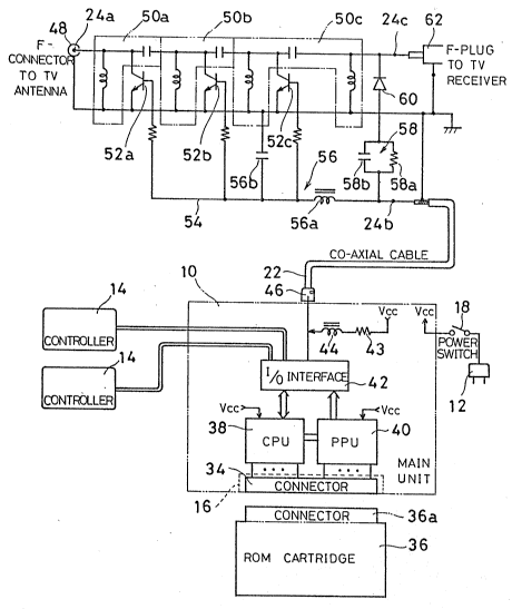
The main unit lO is connected to RF switch 24
through a coaxial cable 22. The RF switch 24 is connected
to an antenna terminal of a conventional TV receiver 28
thro~gh a coaxial cable 26. The RF switch 24 is further
connected to a TV antenna 32 by a feeder cable 30. The RF
switch 24 operates to switch over the input of the
receiver 28, from the TV antenna 32 to the game system
main unit 10 and vice versa.
Referring to Figure 2, the cartridge port 16 of
the main unit 10 is provided with a connector 34. Plugged
into the connector 34 is a connector 36a of the ROM
cartridge 36. In the embodiment, the connector 36a i5
', " . ' , ',
-
. . .
.. .. . . . . . .
5 1323416
formed as a male part arranged wi~h a plurality of pins
and the connector 34 is formed as a female part to receive
these pins. The connector 34 is connected to a CPU 38 and
a PPU 40, for example, by flat cables or other wiring.
The CPU 38 and the PPU 40 are connected mutually as well
as to an I/O interface 42, to which two controllers 14 are
connected.
The CPU 38 provides video picture data necessary
to play the game to the PPU 40 based upon game program
data from a ROM (not shownl included in the ROM cartridge
36 and control signals from the controllers 1~. As the
CPU 38, a microprocessor, for example, such as an
integrated circuit "Z80A" made by Zilog Inc. may be used.
The PPU 40 is for generating the TV signal of NTSC
standard, for example, based upon the picture data from
the CPU 38. As the PPU 40, for example, an integrated
circuit "2C03" made by Nintendo Co., Ltd. may be used.
The picture signal from the PPU 40, that is, the
TV signal is applied to the coaxial cable 22 through the
I/O interface 42. To the coaxial cable 22, a DC control
voltage, for example, of about 3 volts from the AC adapter
12 ~Flgure 1) is also applied through the power switch 18,
a protective resistor 43 and a choke coil 44. The
protective resistor 43 is for protecting the power source
~Vcc) of the main unit 10 even if the main unit 10 at RCA
plug 46 is erroneously short-circuited by an operator. A
res~stance value of the protective resistor 43 i5 selected
relatively high such that it allows current sufficient to
turn on switching transistors 52a-52c to be supplied to
the RF switch 24. The choke coil ~4 prevents the TV
signal ~rom the PPU 40 from flowing into the power line
through the AC adaptor. Thus, the superposed TV signal
from the PPU 40 and the DC control voltage are outputted
to the coaxial cable 22, which is connected to the RF
3~ switch 24.
In the RF switch 24, a first input end 24a is
connected to an F-connector 48 which in turn is connected
to the TV antenna 32 through the feeder cable 30 (F1gure
..
~ ' ' ' ' . . ' , '
- .. . . .
. ' ' ' .
1323416
1). A second input end 24b receives the above-mentioned
coaxial cable 22 and an output end 24c is connected to an
F-plug 62 by a coaxial cable.
Between input end 24a and the output end 24c,
three-stage high-pass filters 50a, 50b and 50c are
connected in cascade. In this embodiment, the high-pass
filters 50a-50c are constructed as ~-type filter. The
output sides of respective filters soa, sob and 50c are
selectively grounded through switching transistors 52a,
52b and 52c to disable, i.e. inactivate, the filters.
These switching transistors 52a-52c are connected to a DC
voltage line 54 via sui~able current-limit resistors. The
DC ~oltage line 54 is connected to the above-mentioned
second input end 24b via a choke circuit 56 including a
choke coil 56a and a by-pass capacitor 56b. The choke
circuit 56 serves as a high-frequency blocking circuit for
blocking the TV signal present at the second input end 24b
from flowing back to the first input end 24a and causing
RF interference to be radiated therefrom.
Between the output end 24c and the second input
end 24b, a series connection of a bias circuit 58 and a
switching diode 60 are connected. The bias circuit 58
includes a parallel circuit of a resistor 58a and a
capacitor 58b, and develops a DC voltage to bias the diode
2~ 60 as well as prevent a direct short-circuit between the
input end 24b and the output end 24c. The capacitor ~8b
is for passing the TV signal from the game main unit 10 at
the input end 24b to the output end 24c through the diode
~o,
~he output end 24c of RF switch 24 is connected
to the F-plug 62 through a coaxial cable. The F-plug 62
i~ connected to an F-connector (not shown) of the antenna
terminal o~ the TV receiver 28.
For the purpose of shielding respective inner
conductors, outer conductors of the coaxial cable 22, the
F-connector 48 and the F-plug 62 are all grounded.
In operation, when the RCA plug 46 is not
connected to the main unit 10, or when it is connected but
', , , - ' ' ' .
}
-. : . . . . .
. . .
. . - .
. . ~, ' , , .
-
1 3234 1 6
the power switch 18 of the main unit 10 is off, that is,
when the TV receiv2r 28 (Figure 1) is not used as the
monitor for the game system, the input end 24b has no
applied signal whatever. Accordingly, the switching
transistors 52a-52b remain off and the diode 60 is also
off. Therefore, the respective filters 50a-50c are not
disabled. In this state, ~he TV signal from the TV
antenna 32 (Figure 1) or a VTR (not shown) applied at the
F-connector 48 to the first input end ~4a, is transmitted
to the output end 24c through the active three-stage
filters 50a-50c and thence to the TV receiver 28 (Figure
1) therefrom through the F-plug 6~. Thus, when the
filters 50a-50c are not disabled, the TV signal from the
~irst input end 24a is given to the TV receiver 28 almost
without attenuation as shown by a plotted line X in Figure
3.
When the RCA plug 46 is connected to the main
unit 10 and the power switch 18 of the main unit 10 is
turned on, the superposed RF signal for the game,
generated by the content of the ROM cartridge 36 and PPU
40, and the DC control signal applied through the power
switch 18, protective resistor 43 and choke coil 44 are
outputted to the coaxial cable 22. The superposed RF and
DC control signals are applied to the second input end 24b
through the inner conductor of the coaxial cable 22. The
DC control signal component is coupled to respective
switching transistors 52a-52c through the choke coil 56a
and the DC voltage line 54. Thus, the switchin~
transistors 52a-52c are turned on and ~he output sides of
the corresponding filters 50a-50c are grounded.
Therefore, the filters 50a-50c are disabled. Accordingly,
even i~ the TV signal is present at the first input end
24a through the F-connector 48, the TV signal will be
grounded through the inactivated filters 50a-50c, namely,
3~ through the switching translstors 52a-52c and
substantially attenuated as shown by a plotted line Y in
Figure 3. The TV signal at input end 24a thus does not
appear at the output end 24c.
- . - : . :
~ .
,
13~3~16
At this same time, the TV signal present at the
second input end 24b is blocked by the choke circuit 56 so
it does not leak back to the first input end 24a ~hrough
the filters 50a-50c.
The DC control signal tDC voltage) present at
the second input end 24b i5 applied to the diode ~0
through the resistor 58a of the bias circuit 58,
generating a forward voltage across the diode 60 of
approximately 0.7 volts. Therefore, the diode 60 is
turned on. The TV signal at the second input end 24b is
passed through the diode 60 via the capacitor 58b of the
bias circuit 58 to the output end 24c, since ~he diode 60
i5 in a low impedance "on" state. The TV signal (RF
signal from the main unit 10 thereby appears at the output
end 24c and is applied to the antenna term~nal ~not shown)
of the TV receiver 28 through the F-plug 62 as in the
previous case.
Thus, by turning on or off the power switch 18
of the main unit 10, the RF switch changes the TV signal
available at the output end 24c. Accordingly, when the TV
game apparatus is not being used, a TV broadcast may be
received by the TV receiver 28. To play the TV game, the
power switch 18 of the main unit 10 is turned on to
automatically disable the TV broadcast signal and to cause
only the TV game signal from the main unit 10 to be
applied to the TV receiver 28.
Figure 4 is a circuit diagram showing a modified
form of certain portions of the main unit 10 of the Figure
2 embodiment. In the Figure 4 embodiment, the I/O
interface 42 includes an RF modulation circuit 42a to
which an output of the power switch 18 is applied through
a slide switch 19 and through a conductive printed circuit
pattern 36a formed in U-shape letter at an edge of the
plug-in board of the ROM cartridge 36. The slide switch
3~ 19 is for turning off the power source to the RF
modulation circuit 42a whlle the power switch 18 remains
in its ON state. The power switch 18 and the slide switch
19 are connected to each other through the conductive
.~ ~
.
1 3234 1 6
pattern 36b only when the connector 36a of the ROM
cartridge 36 is plugged into the connector 84 o~ the main
unit 10. The DC voltage Vcc thus cannot be applied to the
RF modulation circuit 42a even if both the power switch 18
and the slide switch 19 are ON when ROM cartridge 36 is
detached. An RF signal passing from the second input end
24b to an output end 24c is cut off automatically, and the
TV signal from the first input end 24a is applied to the
output end 24c.
Figure 5 is a circuit diagram showing a modified
example of the embodiment of Figure 2 especially the RF
switch. In the embodiment shown, filters 50a, 50b and 50c
are constructed as a T-type filter. Other aspects are
identical with Figure 2 so that duplicate description will
be omitted here.
The RF switch 24 described above may be
incorporated into the main unit 10 or the TV receiver 28,
However, it is preferably constructed separately from
these units as shown in Figure 1.
Now, referring to Figures 6 and 7, the structure
of the RF switch 24 will be described in detail. The RF
switch 24 comprises a housing 64 having a lower shell 64a
and an upper shell 64b mated therewith. The housing 64 is
formed in a plan rectangle and provided therein with a
board 66 having the filter circuit and associated
components as shown in Figure 2 or Figure 4 mounted
thereon. The coaxial cable 22, the F-connector 48 and the
F-plug 62 ~Figure 2) are connected to the board 66. The
F-connector 48, the coaxial cable 22 and the F-plug 62 are
connected respectively to the first input end 24a, the
second input end 24b and the output end 24c as previously
de~cribed.
~s clearly understood from Figure 7, housing 64
i-~ formed with holes 68 and 70 that accommodate the
insertion of the F-connector 48 and the F-plug 62, and a
hole ~2 that serves to guide coaxial cabl~ 22 to the
outside of the housing 64. Along one oE the longer sides
of the housing shells 64a and 64b, channels 74a and 74b
~323416
are formed. Then, in the channels 74a and 74b, a
plurality of protrusions 76a, 76a---and 76b, 76b,---are
formed in a staggered fashion as shown in Figure 6(D).
In the example shown in Figure 6(A), the coa~ial
cable 22 is guided out of the housing in an ortho~onal
direction relative to the long side of the rectangular
housing 64. But, depending upon the arrangement of the
main unit 10 and the TV receiver 28, there may be a case
in which this configuration of the coaxial cable 22 is
lQ impractical. Accordingly, in the embodiment, the coaxial
cable 22 is adapted to be guided out of the housing 64
parallel to the long side thereof by utilizing the
channels 74a and ~4b as shown by the double dotted line in
Figure 6(A). Coaxial cable 22 is held in the channel r~4
by the protrusions ~6a and 76b formed in the respective
channels.
Although the present invention has been
described and illustrated in detail, it is clearly
understood that the same is by way of illustration and
example only and is not to be taken by way of limitation,
the ~pirit and scope of the present invention being
limited only by the terms of the appended claims.