Note: Descriptions are shown in the official language in which they were submitted.
13~3~3~
-- 1 --
Apparatus for Measuring the Thickness of a Thln Fil_
The present invention relates to an apparatus for
measuring the thickness of a thin film.
It is well known that interference fringes can be
observed by projecting a light beam onto a thin film
having parallel top and bottom surfaces and which is
optically transparen~. The thickness of a thin film can
be measured utilizing this interference phenomenon.
Measuring methods for practical use are
classified into two classes as follows:
(1) Method utilizing an interferometer
An interferogram is o~tained by moving a movable
mirror in a system using a Michelson type of interfer-
ometer with white light. The thickness of a thin film can
be estimated by measuring the separation of the central
and side bursts of the obtained interferogram. This
interferogram can also be obtained using an FT-IR (Fourier
Transformation-Infrared) spectrometer for general use.
(2) Method utilizing a wavelength monochrometer
In this system a source of~white light~and a wave-
len~th disperser, such as a diffraction grating or a
prism, is used. The wavelength of the incident light is
mechanically varied and an interference spectrum is~
obtained. This method is essentially same to that
employed in a spectrophotometer of the dispersion type.
:
' ' '
.- `: '
~ 323~34
-- 2
Alternatively, a special interference spectrum generated
by a polychrometer can be measured by a linear array
detector without scanning monochrometer mechanically.
However, both of these methods still have some
S problems to be solved from the view point of practical use
when they are applied to a production line for a thin film
wherein reasonable restrictions ag~inst oscillations and
the environment are required.
In the former method (1), initial adjustment and
precise control of a translational movement of a moving
mirror are difficult and, further, this system is unstable
to mechanical oscillations, and the side bursts of the
interferogram cannot usually be clearly observed.
In the latter method (~), it is difficult to
obtain a reasonable mechanical stability and the high-
speed thickness measuring of running film, since the
monochrometer has to be scanned mechanically. In the
method wherein a linear array detector is used, the
applicable range of wavelength is limited, and a high
sensitivity cannot be obtained; also, the magnification of
the optical system is required to be constant so that a
fast processing time can be obtained.
A key point in a method for accurately measuring
the thickness of a thin film utilizing the optical inter-
~5 ~erence phenomenon is to obtain a clearly distinguishableand sta~le interference fringe pattern.
The visibility of the interference pattern
depends mainly on the transparency of a film to be
measured. For this reason, the films measurable by the
conventional metho~s are limited and restricted. In other
~ords, the methods cannot be applied to a film having a
low transparency, such as a translucent film, or a coating
layer on a metal plate or the like.
In order to extend applicability to various films,
.
. ' .
'
.- ' ~ ' ,
~23~3~
-- 3 --
the choice of a light source is important. Laser is ideal
as the light source, because of its monochromatic and
coherent characteristics, ~irectional property and high
intensity. But, laser light is not applicable to the
methods mentioned above, since it is monochromatic.
Contrary to the above, in USP 4,6~0,980 issued
April 28, 1987 to Hitoshi Takabayashi et al there is
disclosed an apparatus for measuring the thickness of a
thin film wherein a coherent light beam is used to scan
the thin film and the difference between an order of
inter~erence fringes obtained for one scan by the coherent
light beam is counted to detect the thickness of the thin
film.
However, the optical system used in this
apparatus is not easy to adjust, since the scanning
optical system and the detecting optical system are
separately formed. Further it is difficult to calibrate
the angle of the incident beam accurately.
It is an object of the present invention to
provide an apparatus for measuring the thickness of a thin
film with all elements mounted in a housing.
It is another object of the present invention to
provide an apparatus for measuring the thickness of a thin
film, that can obtain a center point of interference
frin~es with resPect to the normal of the film plane.
It is a further object of the present invention
to provide an apparatus for measuring the thickness of a
thin film, that can calculate the thickness using a
relation between adjacent fringes.
It is another object of the present invention to
provide an apparatus for measuring the thickness of a thin
film, that can obtain the thickness by processing data
with a digital circuit.
It is a still further object of the present
inventlon to provide an apparatus for~measuring the
: ~ :
':
,
.
~ 32~3~L
- 4 -
thickness of a thin film, that can correct errors caused
by various fluctuations oE the thin film to be measured.
It is also an object of the present invention to
provide an apparatus capable of measuring the thickness of
a thin film even if it is translucent.
In order to achieve these ob~ects, according to
the present invention, there is provided an apparatus for
measuring the thickness of a thin film utilizing an
interferometric method comprising:
light source means for generating a monochromatic
light beam;
scanning means for scanning the light beam onto a
thin film in such a manner that an incident angle thereto
is continuously varied from a to (-~);
first detection means for detecting said incident
angle oE the light beam;
second detection means for detecting an
interference pattern caused by light beams reflected from
the top and bottom surfaces of the thin film; and
calculation means for calculating the thickness
of the thin film in accordance with a geometrical optical
relation defined between adjacent fringes contained in the
detected interference pattern.
The present invention also provides an apparatus
for measuring the thickness oE a thin film utilizing an
interferometric method, comprising:
light emitting means for generating a mono-
chromatic light beam;
deflecting means for deflecting and scanning the
light beam;
a projecting optical system for projecting the
deflected light beam onto the thin film in such~a~manner
that an incident angle thereof to the thin film is
continuously varied from a to (-a);
: ~ :
: `
~: :
.
.
.
`.` ~
~323~3~
-- 5 --
beam splitter means for splitting the deflected
light beam into a heam impinging onto the thin film and a
reference beam for detecting an angle of the impinging
beam, said beam splitter means being arranged on the
optical axis of the projecting optical system;
a light receiving optical system for detecting an
interference pattern caused by interference between two
light beams reflected from the top and bottom surfaces of
the thin film which is arranged so as to receive two light
beams that have been reflected by said beam splitter means;
angle detecting means for detecting an incident
angle of the inpinging beam defined with respect to a
normal to the thin film; and
calculating means for calculating the thickness
of the thin film based on an arithmetic relation between
t~o adjacent fringes contained in said detected inter-
ference pattern.
It is to be noted that the term "film" should be
interpreted to include not only an actual film, but also
any thin covering or coating irrespective to whether or
not it is transparent.
These and other features oE the present invention
will become more apparent when the preferred embodiment of
the present invention is described in detail with
reEerence of accompanied drawings in which;
Fig. 1 shows an optical system according to the
present invention;
Fig. 2 is diagram showing interference caused by
two light rays;
Fig. 3 is a block diagram of a circuit for
processing signals according to the preferred embodiment
of the present invention;
Figs. 4(a) and 4(b) are a timing chart for
showing the eelation among an interference patteen,
:
'
` ,:,
.
'. ' ' :
.
~1 32~3~
optical and electric signals obtained by slit means and
clock signal qenerating means;
Fig. 5 is a vertical cro~ss-sectional view of an
optical scanning system according to a second preferred
embodiment of the present invention;
Fig. 6 iS a plan view of the system shown in Fig.
5;
Fig. 7 is a diagram for showing a rotational
angle 3' of the first mirror;
Figs. 8 and 9 show interference patterns measured
by the optical scanning system shown in Fig. 5, and
Fig. 10 is a graph showing data obtained from the
interference patterns of Figs. 8 and 9.
(a) Principle utilized in the present invention
As is well known, the reason why an interference
phenomenon is caused by a thin film is based on the fact
that monochromatic light impinging on the thin film is
divided into reflected light and transmitted light by a
boundary surface defined between ambient air and the thin
~0 ilm. When the reflected light and the transmitted light
are superposed, the intensity I of the superposed light is
given by the following equation:
2 2
I = A + B + 2AB cos(2~ /A ) ~ ...(1)
wherein, A, B are the amplitudes of the reflected and
transmitted light, respectively, A is the wavelength of
the incident light and Q is the difference between the
li~ht paths of the reflected and refracted light.
Hence, the intensity I is a function of the phase
difference ~2~Q / A) between the light paths.
As is apparent from equation (1), the intensity I~
of the superposed light varies with the difference a :
between the light paths.
. .
.
, '
,~ :
1323~3~
-- 7
Referring to ~ig. 2 wherein an incident light
beam Io impinges at an incident angle ~ defined to the
normal to the top surface of a thin film F, which has a
bottom surface parallel to its top surface, an optical
path difference ~r between the first and second
reflected light beams Rl and R2, and an optical path
difference at between the first and second transmitted
light beams Tl and T2, are represented b~ the following
equations:
~r = 2nd cos ~ + ~ / 2
=¦2d n2 _ sin2 ~+ ~ / 2 ...~2)
~t = 2nd cos ~ =J2d n2 _ sin2~ ...(3)
wherein, ~ is the refraction angle, n is the
refractive index of the thin film, and d is the thickness
thereo~.
By substituting equations t2) or (3) in equation
(1), the intensity distribution of the interference
pattern is expressed as a function of the incident angle~ .
If the thickness d of the thin film is constant,
~ an interference pattern having bright and dark fringes,
namely peak maxima and minima, is obtained when the
incident angle~ satisfies the following equation (4) or
(S) .
2d ~ si~2 ~ = (2m + 1) ( ~ / 2) ... ~4) ~ ;
` '
.
' : ,~ , ~ ' . . '
~3~3~3~
8 --
2dln2 - sin2 ~ = 2m ( A/ 2) ...(5)
wherein M (=0, 1, 2r . . . ) r being the order of each
interference fringe.
These equations give the conditions for the
maxima and/or minima of the intensity distribution of the
interference fringes. More specifically, equation t4)
~ives hright fringes in the case of reflected light and
dark fringes in the case of transmitted light, and
equation (5) gives dark fringes in the case of reflected
light and bright fringes in the case of transmitted light.
According to equation (4) or (5), if the orders m
of individual interference fringes are identified
explicitly, the thickness d of the thin film can be
calculated, since the refractive index n, the incident
angle ~ and the wavelength A of the incident light are
known. However, it is not easy to identify the order m of
each interference fringe.
To solve this problem, consider equation (4) with
respect to the reflected light, assuming that the
~o wavelength A is constant.
Consider the adjacent p-th and (p+1)-th bright
fringes from the innermost of angular radius ~p and
ap~l, respectively. In this case, the following
equ~tion is easily obtained from equation (4):
~5 ~d( ~n~ - sin2 ~p /n2 _ sln ~ p~l) = A ...(6)
As is appaeent from equation (6), the order of
fringes does not appear explictly therein~ Accordingly,
.,
- ~ . .
. - : ~ . . :
. : . ,'' ' ' ~ '; `
.
- -
~323~34
if the incident angles ~p and ~p+l which cause p-th
and (p+l)-th bright fringes from the center are deter-
mined, the thickness d can be determined from equation (6).
(b) Composition of the optical system
In an apparatus for measuring the thickness of a
thin film, the film is scanned by a light pencil which is
deflected by a rotating mirror so as to vary the incident
angle of the light beam on the thin film. By this scan,
an interference pattern is obtained and the thickness can
be calculated based on the maxima and minima of fringes
from equation (6).
Fig. 1 shows an optical system that is sub-
stantially comprised of a light source L for generating a
monochromatic liqht beam, such as a laser beam, a rotating
mirror PM for deflecting the beam, fiest and second lens
means Ll and L2 forming a point-to-point image converter,
wherein the first lens means Ll converts a divergent beam
to a parallel beam and the second lens means L2 converts
the parallel beam to a convergent beam, a beam splitter HM
such as a half-mirror interposed between the first and
second lens means Ll and L2 for splitting the light beam
into a measuring beam impinging onto the thin film F and a
reference beam for checking the incident angle of the
impinging beam, a first detector Dl with a collecting lens
means L3 for detecting the intensity distribution of
optical interference fringes, a grid S2 consisting of a
succession of slits formed on an opaque screen, and a
second detector D2 with a collecting lens means L~ for
checking the incident angle of the impinging beam.
The monochromatic light beam emitted from the
light source L, such as a He-Ne gas laser or a laser
diode, is collimated by a collimating lens means C, so
that an incident beam emerges as a sma1ler parallel pencil
of about lQ0 ~m diameter and is then reflected by a
.' ' , ' : ~ ~ ~ :
': ~' ' ~ :.-'
,
1323~
-- 10 --
mirror M and directed to the center point of the rotating
mirror PM, which is the focus of the lens means Ll.
The light beam reflected by the rotating mirror
PM is made parallel to the optical axis by the first lens
means Ll, and then passes a slit means Sl for restricting
the scanning angle within a predetermined range, and is
split into two beams by the beam splitter HM.
A measuring beam transmitted through the beam
splitter HM is ~ent by the second lens means L2 to impinge
onto a point on the surface of the thin film that is set
on the focal plane of the lens means L2, i.e. the incident
point coincides with the focus of the lens means L2.
Reflected beams from the top and bottom surfaces of the
film are made parallel to the optical axis by the lens
lS means L2, and then reflected by the beam splitter HM and
collected onto the first detector Dl by the collecting
lens L3.
On the other hand, the beam splitter HM reflects
a part of the incident light beam as a reference beam
towards the second detec~or D2 through the collecting lens
means L4. Between the beam splitter HM and the second
detector D2, the grid means S2 is interposed in order to
generate clock pulse signals, each corresponding to a
specific predetermined incident angle of the light beam
generated by the rotating mirror PM. These clock pulse
signals are detected by the second detector D2 which is
arranged at the focus of the lens means L4.
Further, a third detector D3 is provided for
detecting the start timing of~the scanning span by the
light beam.
In accordance with the rotation of the rotating
mirror PM, the incident angle ~ is varied at a pre-
determined constant angular velocity symmetrically with
respect to the common optical axis which usually coincides
. :
-- . .
;
-11
with the normal to the thin film plane.
The 5 tructures of the slit means Sl and the grid
means S2 are disclosed in (C) and (D) of Fig. 4(a),
respectively.
The first slit means Sl has a wide aperture a
for restricting the incident angle to within a
predetermined range, and two slits ss and sf for
respectively determining the start timing of a scanning
span and the stop timing thereof.
The grid means S2 has seven slits from bl to
b7 formed at a predetermined constant pitch in its
central portion which corresponds to the aperture al of
the slit means Sl, and two other slits a2 and a3
formed outside the slits bl - b7, which are
lS respectively optically equivalent to the two slits ss and
sf of the slit means Sl.
The slit ss of the slit means Sl gives the start
timing for starting to count clock pulses CLK, and the
slit sf gives the stop timing for finishing this counting
operation.
The seven slits from bl to b7 are provided in
order to check the scanning time by the light beam,
namely, they give time reference signals T(bl) to
(b7).
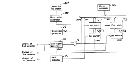
~c) Electric circuit for processing detection signals
Fig. 3 shows a block diagram of the electric
circuit for processing detected signals.
In order to synchronize all operations with a
standard clock pulse signal CLK, there is provided a clock
pulse generator CG. Standard clock pulse signals CLK
generated ~y the clock pulse generator CG are sent to a
motor driving control circuit MP for generating motor
pulses to be applied to a motor driver MD for a rotating
mirror motor (not shown). These clock pulses are also
1'~ ``
'
: .
~323~3~
- 12 -
applied, via an AND gate G, to the inputs of first and
second counters CNTl and CNT2 for counting such pulses.
Parallel outputs of the first and second counters CNTl and
CNT2 are connected, via first and second latches LTl and
LT2, to a microprocessor MC.
Respective temporal count values of the first and
second counters CNTl and CNT2 are latched into the first
and second latches LTl and LT2 by enable signals from the
first and second detectors Dl and D2, respectively. The
latched data are read into the microprocessor MC when
interrupt re~uest signals IRP1 and IRP2 are acknowledged,
respectively.
The counting operations by the first and second
counters CNTl and CNT2 are carried out during a
preselected span interval determined from the start signal
T(ss) given by the slit ss to the stop signal T(sf) given
by the slit sf.
A gate signal generator GG selects only the start
slit signal T(ss) and the stop slit signal T(sf) from
among all the signals sent from the second detector D2 and
outputs these two signals as gate signals to the AND gate
G. In other words, reference slit signals T(bl),
Tlb2),..., T(b7) generated by the seven reference
slits from bl to b7 are masked by the gate signal
2S generator GG.
The output signal of the first detector Dl is
applied to a peak detector PD. The peak detector PD
discrimates individual peak maxima p(mi) of interference
fringes and outputs pulse signals T(mi). By each of the
pulse signals T(mi), a count value CV {T(mi) } of the
first counter CNTl at that time is latched into the first
counter CNTl and then latched data CV { T(mi) } is read
into the microprocessor MC by an interrupt servlce routine
caused by an interrupt request si;gnal IRPl. ~ :
.' ' ' , .
.
- ' . ~'' ' ~' ' ' .
. . .
. . ~. ,,, ' , ' ,
1323~
- 13 -
The count data CV { T(mi) } read into the
microprocessor MC corrresponds to an incident angle
9(mi), since the relation between the count data CV
{ T(mi)} and the incident angle ~(mi) is deterrnined
beforehand to be one to one.
Be each of the reference slit signals from the
second detector D2, a count value CV { T(bi) } of the
second counter CNT2 at that time is latched into the
second latch LT2 and the latched data CV { T(bi)} is
read into the microprocessor MC when an interrupt request
signal I~P2 is inputted thereinto.
The output signal of the third detector D3 is
used as a start signal of the scan cycle by the rotating
mirror PM and, therefore, is used to reset the first and
second counters CNTl and CNT2 and the gate signal
generator GG. Further, it is used as an interrupt request
signal IRP3 to the microprocessor MC.
~d~ Measurement of the thickness of a thin film
Referring to Figs. 1, 3 and 4, the measurement of
the thickness of a thin film will be explained.
At first, a scan cycle is initiated by a signal
from the third detector D3, which is an interrupt r quesc
signal IRP3 to the microprocessor MC to execute a scan
cycle routine.
The first and second counters CNTl and CNT2 and
the qate siqnal generator GG are reset by the signal from
the third detector D3.
Since the light beam is~divided by the beam
splitter HM, a part of the light beam that has passed
through the scan start slit ss of the~slit means Sl passes
throuqh the scan start slit a2 of the grid means 52.
When the second detector D2 detects the part of
the liqht beam that has passed through the scan start slit
a2 of the grid means S2, the gate pulse generator GG out-
: :
:
:
:: ~
`; : :
:
.
.
: ,, .
. . .
~23~3~
- 14 -
puts a gate pulse to the AND gate G. The AND gate G
allows clock pulse signals CLK from the clock generator CG
to pass therethrough and, therefore, the clock pulse
signals CL~ are counted by the first and second counters
CNTl and CNT2 respectively.
As stated above, the reference slits from b
and b7 formed on the grid means S2 correspond to
predetermined incident angles to the thin film F and,
therefore, aee utilized for checking real incident angles
to be detected by the first detector Dl. Namely, the
light beams that have passed through the reference slits
bl to b7 are detected by the second detector D2.
Accordingly, pulse signals T(bl) to T(b7) from the
second detector D2 correspond to specific predetermined
incident angles, respectively, and a temporal count value
CV { T(bi) } of the second counter CNT2 at that time
T(bi) is latched into the second latch LT2. The latched
count data CV { T(bi) } is read into the microprocessor
MC by an interrupt service routine caused by interrupt
~0 request signal IRP2. These count data CV { T(bi)~ are
used to check the real incident angles that are
predetermined by use of a standard sample.
When the light beam that has passed through the
scan stop slit a3 of the grid means S2 is detected by
~5 the second detector D2, the gate pulse generator GG
disables the AND gate G and terminates one scan.
Similarly to the above, the next scan cycle is started.
The light beam that has passed thrcugh the -
aperture al of the slit means Sl, the beam splitter HM
and the second mirror L2 impinges on the thin film F.
This light beam is scanned on the thin film F at a
constant angular velocity varying the incident angle~
from (~) to (-~) according to the rotation of the mirror
P~. Due to this laser scan, the output signal of the
. . .......... , ~ . ,, ; . ' '
' '. ' . . . .
-.. .: : :' ' ' . ,
`` - . , . : . :
1323~3~
first detector Dl shows an interference pattern (H) in
Fig. 4(b). More specifically, the start signal T(ss) has
passed through the scan start slit ss of the slit means Sl
at first, and then the interference fringe mi and the
stop signal T(sf) has passed through the scan stop slit s~.
The peak detector PD detects peak maxima (mi)
of the interference pattern obtained and outputs enable
signals T(mi) to the first latch LTl and an interrupt
request signal IRPl to the microprocessor MC.
By each o~ the enable si~nals T(mi), a count
data CV { T~mi) } of the first counter CNTl at that time
T(mi) is latched into the first latch LTl and the
latched count data CV { T(mi)} is read into the micro-
processor MC when an interrupt request signal IRPl is
acknowledged.
The microprocessor MC processes these count data
CV {T(mi) } to obtain the thickness of the thin film to
be measured using a predetermined relation between the
count data CV { T(mi) } and the incident angles ~(mi)
at the time T(mi) that is provided by a calibration or
transformation table TBl for transforming the count values
into corresponding incident angles in the present
preferred embodiment. This table is made based on an
analysis of an interference fringe pattern obtained using
~5 a standard sample whose refractive index and thickness are
~nown and is memorized in a ROM (Read Only Memory) of the
microprocessor MC.
Also, one more transformation table TB2 is
prepared in order to determine the relation between each
oE the reference count values CV {T(bi) } and the
incident angle~ . This relation is determined based on an
interference fringe pattern meaaured by the first detec~or
Dl using a standard thin film whose refraction index and
thickness are known. In other words, each incident angle
.
' ' . ................... . . .
,
~323.~34
- 16 -
corresponding to each count data CV { T(bi)} is
calcula~ed theoretically ~rom data of the interference
fringe pattern obtained. Thus, each incident angle
corresponding to each count data CV { T(bi)} is
S determined with utilization of this table TB2 in order to
check the real incident angles obtained by the trans-
formation ta~le TBl . This table TB2 iS also memorized in
the ROM o the microprocessor MC.
Calculation of the thickness of a thin film is
done as follows.
As mentioned above, each count data CV { T(mi) }
corresponding to each peak maximum mi (bright fringe) of
an interference pattern obtained has been read into the
microprocessor MC.
If a thin film to be measured is set
perpendicularly to the optical axis of the scan system,
each count data CV { T(mi) } is transformed into an
incident angle ~i referring to the standard trans-
formation table TBl.
~o According to equation (6) representing the
relation between the adjacent p-th and (p+l)-th maxima
from the center of the fringes, the thickness d is
obtained as follows:
d = (~ / 2) / ~ ~ n2-sin2~p - ~n2-sin2~p+l]...(7)
~5 Since the wavelength A of the laser and the
re~ractive index n of the thin film are known, the
thickness d is calculated from the adjacent incident
angles ~p and ~p+l
Usually, the interference pattern includes a
plurality of fringes as shown by (H) of Fig. 4(b).
~ccordingly, it is desirable to take an average with
respect to a plurality of thicknesses obtained from plural
:~23~3~
adjacent pairs of fringes (ml, m2), (m2, m3),....
(~p, mp+l) in order to enhance the accuracy oE
measurement. ~urther, when the thin film is set
stationary at the focal plane of the lens means L2, it is
desirable to repeat the optical scan by rotating the
mirror PM in order to take a multiple average with respect
to the averages obtained by the respective scan cycles.
This further contributes to enhancement of the accuracy of
measurement.
It is to be noted that the thin film is not
always set perpendicular to the optical axis of the scan
system. Especially in the case of a moving film vertical
and/or angular fluctuations are inevitable.
In view of this point, the thickness measuring
lS system is desired to be a system that is stable against
film fluttering movement or able to correct errors caused
thereby.
In order for this result to be achieved, the
scanning speed of the light beam, which is determined by
the rotation speed of the rotating mirror (and/or a number
of mirrors) should be chosen to be fast enough to tolerate
film flutter movement without noticeable effect. This is
the most effective way to avoid the need for complex
processing for correcting errors due to film
~5 fluctuations. Although the incident angle to a thin film
plane is not varied by a fluctuation thereof in the
vertical direction, the path of the light reflected from
the thin film when it fluctuates in the vertical direction
is shifted from that obtained when the film is set
3~ correctly. This shift can be made allowable within a
certain range by using a first detector Dl that has a
relatively larger photo-receiving area.
Since it is not necessary to measure a special
interference fringe pattern in the system according to the
. " ' , ` '
.
. ~ ' . ,
-
.
~3~3~
- 18 -
present invention, the measurement is not affected by the
magnification or distortion of each of the lenses used in
the optical scan system.
With respect to any angular fluc~uation of the
thin film, namely an angular shift of the normal of the
thin film from the optical axis of the scan system, it is
possible to correct errors caused thereby by using
suitable algorithmic processing, since the detected
interference pattern includes data with respect to the
angular shift.
Namely, in this algorithmic processing, the
center of the measured interference fringes is first
sought, utilizing the symmetry that every set of
interference fringes always shows. This center of
symmetry of the interference fringes corresponds to an
incident angle of 7.ero degree, namely a timing at which
the light beam impinges vertically onto the thin film
plane.
The angular shift can be sought using the shift
amount of the center of symmetry from the correct center
of symmetry. Thereafter, every count value of standard
clock pulses corresponding to each peak maximum is
corrected, based on the sought angular shift. The
thickness of the thin film can thus be calculated exactly
~5 using the corrected incident angles.
If the present measuring system is applied to
measuring the thickness of a thin film being produced, it
is mounted on a carriage on a single side o the film
which can be moved in a direction traverse to the travel
of the moving film in order to measure the thickness over
the whole width of the film.
The present measuring apparatus employed ln film
thickness gaging can be operate in the oper, on refl0cted
radiation, making it possible to mount the entire
:: :
'
~32~3~
-- 19 --
apparatus on a single side of the film process.
Figs. 5 and 6 are a vertical cross-sectional view
and a plan view of a scanning optical system according to
the second preferred embodiment of the present invention,
respectively~
In this second embodiment, three mirrors ~1, M2
and M3 are used for scanning a monochromatic light beam
emitted from a laser L.
The mirror Ml is a plane mirror for deflecting
the beam onto the second mirror M2 which is comprised of a
eylindrical mirror that is arranged with its central axis
~A coinciding with the point of reflection of the light
beam by the mirror Ml. The mirror Ml is supported on an
axis (not shown) that coincides with the central axis CA
of the mirror M2 and is rotatable around this axis at a
predetermined angular velocity by a suitable driving
mechanism (not shown).
The mirror M3 is a plane mirror for reflecting a
beam reflected from the mirror M2 onto a thin film F, and
2~ for reflecting a beam reflected from the thin film F onto
a photodetector D that is arranged to have its detecting
surfaee coincident with the axis CA. The center of the
mirror Ml is positioned at a height ~ from the center of
the cylindrical mirror ~2.
As shown in Fig. 6, the cylindrical mirror M2 has
a radius r and, as shown in Fig. 7, a rotation angle ~' of
tl~e mirror Ml is defined with respect to a horizontal axis
passing through the center thereof. -
Figs. ~ and 9 show interference patterns obtained
3~ when two thin films of PET ~n = 1.5) having eespective
nominal thieknesses of 16 and 12~m are measured using
this scanning optical system.
The method for calculating the thickness of the
thin filn is substantially same to that mentioned above.
.. ~
.
, ' , .:
.
. .
- , . ' ' , . . ' . .
~2~3~
- 20 -
However, in the second emhodiment, all of the bright and
dark fringes obtained are used to calculate the thickness
more accurately.
Assume that each of the bright and dark fringes
is numbered in ascending order from the innermost fringe
ml, as shown in Fig. 8 or Fig. 9.
Using equations (4) and (S) above, the relation
between the innermost fringe ml and the i-th fringe
therefrom is given by the following equation:
10¦ n2 _ sin2 ~ml + i = _ (ml + i) (7)
4d
wherein n is the refractive index of the thin
film to be measured, ~ is the wavelength of the light
beam, and ~(ml + i) is the incident angle of the light
beam corresponding to the i-th fringe from the innermost
bright fringes ml.
The incident angle ~ is calculated from the
rotational angle ~' of the mirror Ml by the following
equation, as will be easily understood from a geometrical
consideration of the optical scanning system according to
~0 the present embodiment.
Q
. 2 ~ 2r + sin2 2 9~
. . . ( a )
wherein Q, r and ~' are already defined in Figs.
5, 6 and 7.
Fig. 10 shows data plotted with respect to each
of the interference patterns. These were obtained under
~5conditions of r = 44.9 mm, Q = 4.75 mm, n - 1.5, ~
0.6328 ~m (He-Ne laser ? and a rotation speed of~the mirror
::
-
- ' . . ' ' ' ' '
~L323~34
- 21 -
Ml = 1800 rpm.
These data are processed using the least square
approximation in order to evaluate the slope (- ~/4d) in
equation (7). The slopes obtained are (-0.0102) and
(-0.0132), respectively, and, accordingly, the thicknesses
calculated from them are 15.5 ~m and 12.0 ~m, respectively.
The preferred embodiments described herein are
illustrative and not restrictive, the scope of the
invention being indicated by the appended claims and all
variations which come within the meanings of the claims
are intended to be embraced herein.
:
: ~
: ' ' . :