Note: Descriptions are shown in the official language in which they were submitted.
1 323440
BACKG~OU~D OF THE INVENTION
The invention relates to fault tolerant
digital data processing and, particularly, to
5 apparatus and methods for prov~ding fault tolerant
communications with peripheral devices.
Faults in digital computer systems are
inevitable and are due, at leas~ in part, to the
comple2ity of the circuits, the associated
10 electromechanical devices, and the process control
software. To permit system operation even after the
occurrence of a fault, the art has developed a number
of fault-toleran~ designs~ Among these is Rennels,
"Architecture for Fault-Tolerant Spacecraft
15 Computers,~ Proc~edings of the I.E.E.E., Vol. 66, No~
10, pp. 1255-1268 (1975~, disclosing a computer
system having independent self-checking computer
modules (SCCM's). In the event of failure of a
module, the SCCM is taken off-line.
An improved fault-tolerant digital data
processing system is currently available from the
assignee hereof, Stratus Computer Company, of
Marlboro, Massachusetts. This system employs
redundant functional unit pairs, e.g., duplicatiYe
25 central processing units, duplicative memory units,
and duplicative peripheral control units,
interconnected for information transfer by a common
system bus.
The aorementioned system bus includes two
30 duplicative buses, the A Bus and the B Bus, as well
as a control bus, the X Bus. During normal
operation, signals transferred alonq the A Bus are
duplicated through simultaneous transmission along
the B Bus. Signals trans~erred along the X Bus,
1 323440
including timing, status, diagno~tics and
fault-responsive signals, and are not duplicated.
Within the Stratus System, control of and
communications with peripheral devices-are effected
5 by peripheral control units. One such unit, the
communication control unit, routes control and data
signals to attached peripheral devices by way of a
communication bus.
With this background, an object of this
10 invention is to provide an improved digital data
processing system. More particularly, an object of
this invention is to provide a system for improved
fault-tolerant communication with, and control of,
peripheral devices.
A further object of this invention is to
provide an improved fault-tolerant bus structure for
use in di~ital data processing apparatus and,
particularly, for use in communications with data
processor peripheral units.
Yet another object of this invention is to
provide an input/output controller for controlling
and communicating with plural peripheral devices over
a common peripheral bus structure.
Other objects of the invention are evident
25 in the description which follows.
,
,
.
` '
1 323440
SUMMARY OF THE INVENTION
The aforementioned objects are attained by
the invention which provides, ;n one aspect, an
5 improved fault-tolerant digital data processing
system having a first input/output controller which
communicates with at leas~ one peripheral device over
a peripheral device bus. The peripheral bus means
includes first and second input/output buses, each
10 including means ~or carrying data, address, control,
and timing siqnals.
The input/output controller încludes an
element ~or applying duplicate information signals
synchronously and simultaneously to the first and
15 second input/output buses for transfer to ths
peripheral device. That is, upon applying
information signals to the first input/output bus,
the input~output controller simultaneously applies
those same signals to the second input/output bus.
~0 In a further aspect, the invention provid~s
a fault-tolerant digital data processing system of
the type described above in which the input/output
controller includes a bus interface element for
receiviny, in the absence of fault, duplicative
~5 information signal synchronously and simultaneously
from the first and second input/output buses.
Still further, the invention provides a
digital data processor of the type describe above in
which the input~output controller includes clocking
30 elements for qenerating and transferrinq on the first
and second input~output buses strobe signals
indicative of the timing of associated information
transfers along those buses.
1 323440
-- 4
The aforementioned input/output controller
can also include a scanner element for polling the
peripheral devic~s ~hich are connected along the
peripheral device bus. By ~his polling, the scanner
5 can determine the current opera~ional status of each
peripheral device. Using this scanning element, the
input/output controller can determine, for example,
whe~her a periphera~ is acti~e and awaiting
instruction, whether it requires interrupt
10 processing, or whether it has become unexpectedly
inactive.
According to another aspect of ~he
invention, a digital data processor having a first
input/output controller communicates with one or more
15 peripheral devices over a peripheral device bus
having first and second input~output buses for
carrying, respectively, first and second input
signals. In the absence of $ault, these first and
second siqnals are identical and are transmitted
20 synchronously and simultaneously along those buses.
The aforementioned input/output controller
can include first and second processing sections,
each for processing signals received on the
peripheral device bus. During the course of normal
25 operation, the first and second processing sections
receive identical input signals from the peripheral
bus and produce identical output signals.
Further, a first bus ;nterface element can
be coupled with the processing sections and with said
30 peripheral bus for receiving the first and second
input signals and for applying at least one ~f those
input si~nals identically, i.e., synchronously and
simultaneously, ~o said first and second processing
sections.
B
~. . .
1 323440
- 5
A digital data processor of the type
described above ca~ also include a second peripheral
controller whic~ is coupled with the peripheral
device bus for receiving the first and second input
5 signals identically with the first peripheral
controller. In this aspect, a second device
interface element serves to apply at least one of
those input signals to said second input/output
controller.
In order to coordinate operations of the
first and second processing sections, the data
processor can include a flash circuitry element that
is coupled to the first and seçond bus interface.
This circuitry is responsive to operational states of
15 the bus interface elements for generating a signal
indicative of the synchronous receipt of identical
copies at least one of the first and second input
signals by each of said first and second bus
interface elements.
Thus, the flash circuitry provides a
mechanism by which the digital data processor can
insure that the first and second bus interface
sections are simultaneously applying duplicative and
synchronous information signals to th~ first and
25 second processing sections of the first peripheral
controller, as well as to the second peripheral
controller.
In still anotAer aspect, a digital data
processor as described above can utilize bus
30 interface elements for appl~ing duplicative outpu~
signals synchronously and simultaneously to the ~irst
and second input/output buses. Wi~hin such a
processor, flash circuitry can be advantageously
employed to monitor those transmissions.
' ~ ~
.
.' ' ' . ' .
.
.
,
- 6 - 1 32 34 4 0
According to this aspect of the invention,
the flash circuitry can generate a timing signal,
which itself is ~ransmitted along the first and
second input/output buses, indicat;ve of the timing
5 of information transfer cycles along the bus.
Consequently, for e~ample, a peripheral device
attached to the bus can employ an interface for
inputting transferred signals only at the time of
receipt of the transmitted strobe signal. Through
10 this mechanism, the peripheral avoids the processing
of non-duplicative or asynchronous information
signals.
The flash circuitry of a digital data
processor as described above can include, further, a
15 strobe delay element which responds to differing
operational states of the first and second bus
interface elements for delaying generation of the
aforementioned STROBE signal. This delay ele~ent can
be employed to facilitate continuous operation
20 notwithstanding a slight delay in the receipt of
either of the first and second information signals
along the peripheral bus structure.
The flash circuitry can also employ an
element for periodically and repeatedly comparing the
25 operational states of the first and second bus
interface elements in order to detect the concurrence
of the first and second information signals. In the
event those signals do not agree after a specified
time period, the processing sections can initiate an
30 error detection sequence to determine the source of
fault.
` Another aspect of the invention provides a
fault-tolerant digital data processing system having
a first input~output controller which communicates
~ .
.
- ' ` ' ' . ' ' ':
.
.
1 323440
-- 7
wi~h at least one peripheral device over a peripheral
device bus, w~i~h includes first and second
input/output buses. AS abo~e, each of these buses
can carry data, address, control, and timing signals
5 from the input/output controller to the peripheral
device.
According ~o this aspect of the invention, a
device interface is coupled to said first and second
input~output buses means and to an associated
10 peripheral device for transferring information
between said the buses and the associated peripheral
device. In normal operation, the device interface
applies duplicate information signals synchronously
and simultaneously to the input~output buses for
15 transfer to said input/output controller.
In a related aspect of the invention, the
device interface includes a bus interface section for
receiving, in the absence of fault, duplicative
information signal synchronously and simultaneously
20 from the first and second input~output buses.
The interface can include a fault detection
element that is coupled to said bus interface for
detecting faulty information transmission and for
responding thereto to generate a fault signal.
25 According to this aspect of the invention, the device
interface can respond to a first selected type of
transmission error, e.g., a single-bit error,
occurring on one of the buses for accepting data only
from the other bus. Similarly, the device interface
30 can respond to a second selected error type, e.g., a
multi-bit error, occurring on either bus for
initiating a diagnostic testing se~uence.
The aforeme~tioned testing sequence~can
include the timed gen-ration of v-rious diagDostic
'
.
1 323440
testing signals, which are intended ~o facilitate the
identification of the source of error. By way of
example, subsequent to the ~etection of a mul~i-bi~
error, a transmitter portion of the device interface
5 can apply ~assert~ signals -~ i.e., all one's or
zero's -- to the peripheral bus data and function
code conductors for a specified time interval.
Concurrently, a receiver portion of the interface can
monitor the bus to determine whether all the incoming
10 signaIs retain their asserted values.
In another aspect, the invention is directed
to a protocol for communications over the peripheral
device bus of a digital data processor. The
apparatus includes a peripheral device controller for
15 communicating with one or more peripheral devices
over a peripheral device bus which includes first and
second input~output buses, each carrying data,
address, control, and timing information. Each
peripheral device can include a device interface
20 element for transferring information signals between
the associated peripheral device and the peripheral
bus.
According to the aforementioned aspect of
the invention, the peripheral device controller
25 includes a strobe element connected with the first
and second input~output buses for transmitting
thereon duplicative, synchronous and simultaneous
strobe signals. These strobe signals define the
successive timing intervals for information transfers
30 along the peripheral buses.
Further, the peripheral device controller
can include an element for executing an informa~ion
transfer cycle which normally, i.e., in the absence
of fault, involves the transmission o duplicate
9 1 3234~0
information signals synchronously and simultaneously
on said fiIst and second input/output buses. This
transfer cycle element can include a scanner cycle
element to determine an operational state of at least
5 one of the peripheral devices connected to said
peripheral bus; a command cycle element for executing
a command cycle for controlling operation of an
attached peripheral device; a read cycle element for
effecting the transfer of data signals from the
10 peripheral device ~o the input~output controller; and
a write cycle element for transferring data signals
from the input/output controller an attached
peripheral device.
Each of the aforementioned scanner cycle,
15 command cycle, read cycle, and writ~ cycle elements
can include, further, a cycle initiation section or
initiating an information transfer cycle. In this
aspect, the cycle initiation section includes an
element for transmitting, during a first timing
20 interval, a SELECT signal indicative of cycle
initiation. This SEL~CT signal is transferred
duplicatively and synchronously on said first and
second input/output buses. Concurrently, the cycle
initiation section transmits on both buses a SLOT-ID
25 signal indicative of at least one said peripheral
device to be addressed during the information
transfer cycle.
In an apparatus constructed according to
this aspect of the invention, an addressed peripheral
30 device responds to a selected ~LOT-ID signal to
transmit a signal representative of the operational
status of the peripheral device (including its
associated bus interfacs element). This status
signal is transmitted in a second, subsequent timing
1 323~0
- 10 -
interval. Durin~ ~hat ~ime interval, a receiving
element within ~he cycle initiation section receives,
in absence of error, the status signal on both the
first and the second buses.
In related aspects, the inv~ntion is
directed to a digital data processor of the type
described above in which the command cycle element
transmits duplicative command signals along the first
and second buses in a third timing interval.
lQ Alternatively, the processor can utilize
either of the read or write cycle elements to
transmit addressing information during the third,
fourth, and fi~th timing intervals. According to
these aspects of the invention, a write cycle element
15 can thereafter transmit duplicative WRITE signals,
along with duplicative write data, to an addressed
peripheral device. Similarly, a read cycle element
can transmit duplicative READ signals to invoke the
duplication transfer of read data from the addressed
20 peripheral device.
In yet further aspects, the invention is
directed to a peripheral device interface for
responding to and participating in the bus protocol
defined by the actions of the peripheral device
~5 controller discussed above.
In still further aspects, the invention is
directed to methods of operating a digital data
processor in accord with the ~unctionin9 of the
apparatus described above.
These and other aspects of the invention are
evident in the drawings and the detailed description
below.
.. .
1 323440
BRIEF DES~RIPTIQN OF THE DRAWINGS
A more complete understanding of the
inv~ntion ~ay be obtaine~ by reference to the
drawings, in which:
Figure 1 illustrates a digital data
processing systam including a fault tolerant
peripheral i/o system constructed according to a
preferred practice of the invention;
Figure 2 illustrates an i/o controller
10 constructed in accord with a preferred practice of
the invention;
Figure 3 illustrates a flash circuitry
element constructed in accord with a preferred
practice of the invention;
lS Figure 4 illustrates a preferred
configuration of circuitry used to generate
pre-strobe signals;
Figures 5A and 5B illustrate preferred
circuitry for generating strobe signals;
Figures 6A and 6B illustrate preferred
circuitry for generating bus obey signals;
Figure 7 illustrates one preferred circuitry
for generatin~ bus and time-out error signals;
Figure 8 illustrates a timing sequence for
25 preferred command and scann~r cycles;
Figure 9 depicts a timing seguence ~or a
preferred peripheral i/o write cycle;
Figure 10 depicts a timing sequence for a
preferred peripheral i~o read cycle;
~iqure 11 illustrates a timing seguence for
two normal peripheral bus interface cycl~s;
Figure 12 illustrates a timing sequence for
a peripheral bus in~erface cycle including two
peripheral-bus/flash-bus comparisons;
.
- 12 1 32 34 40
Figure 13 depicts a timing sequence for a
preferred bus in erface in which the i/o controller
switches bus obey modes;
Figure 14 illustrates a time-out sequence in
5 a preferred i/o controller constructed according to
the invention;
Figure 15 depicts preferred circuitry for
interfacing a peripheral device wit~ the peripheral
bus;
Figures 16 and 17 illustrate preferred ~us
in~erface circuitry for preferred gate arrays
constructed in accord with the invention;
Figure 18 depicts preferred circuitry for
generating strobe trac~ing signals in a device
15 interface constructed according to the invention;
Fiqure 19 illustrates a preferred circuit
for detecting faults in incoming data signals in a
device interface constructed according to the
invention;
Figure 20 illustrates a preferred circuit
for comparing function code signals received by
partnered qate arrays;
Figure 21 illustrates a preferred circuit
for comparing data signals received by partnered gate
25 arrays;
Figure 22 illustrates preferred circuitry
for checking data and function code signals received
during the stages of the gate array error checking
sequence;
Figure 23 illustrates preferred circuitry
or e~tracting peripheral deYice address information
from the peripheral bus data signals ;n a device :
interface constructed according to the invention;
~ .
;
::
. ' -
' ` : ' ` ' `
`', .
- 13 - 1 323440
Figure 24 depicts preferred circuitry for
generating signals for initiating an error seguence
in a device interface const~ucted according to the
invention;
Figure 25 illustrates preferred circuitry
for extracting peripheral device adaptor command
signals in a device interface constructed according
to the invention;
Figure 26 illustrates preferred circuitry
10 for evaluating slot-id signals received from the i~o
controller:
Figures 27 and 28 illustrate preferred
circuitry for generating gate array s~ate signals in
a device interface constructed according to the
15 invention;
Figure 29 illustrates a preferred circuit
for generating peripheral adaptor control signals in
a device interface constructed according to the
invention;
Figure 30 illustrates preferred circuitry
for generating timing signals in a deYice interface
constructed according to the invention;
Figure 31 illustrates a preferred circuit
for generating adaptor address and data signals in a
25 device interface constructed according to the
invention;
Figure 32 illustrates preferred circuitry
for comparing peripheral bus data signals generated
by partnered gate arrays;
Figures 33 and 34 illustrate preferred
circuitry for generating interrupt-related and obey
signals in a device interface constructed according
to the invention;
'
. .
. . , . ' . . .
- 14 - 1323440
Figure 35 illustrates preferred circuitry
for generati~g start-up signals in a device interface
constructed accor~ing to the invention;
Figure 36 illustrates a preferred circuit
5 for generating timer signals;
Figure 37 illustrates preferred circuitry
for driving data and status signal~ onto the adaptor
bus in a device interface constructed according to
the invention; and
Figure 38 illustrates preferred circuitry
for generating early read and write signals.
::
:::
- ,
. ~, .... .. ~ .' ,' '' ` : ' " '
.. . . . . .. . .
. .
, -: :
,. . .
.
- `, ' ' . ': .
- 15 - 1 3 23~ 40
DESCRIPTION OF THE ILLUSTRATED EMBODIMENT
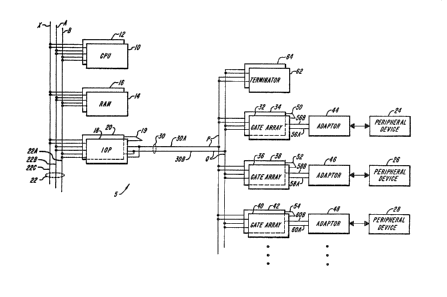
Figure l depicts a digital data processing
system 5 haYing a ~ault tolerant peripheral
5 input/output system constructed according to a
preferred practice of the invention. The system 5
includes partnered central processing units lO, 12,
partnered random access memory unites 14, 16, and
partnered input/output controllers 18, 20, connected
10 for communications over system bus 22.
The i/o controllers 18, 20, which are
coupled via flash bus l9, control the transfer of
information and control signals between the system
backplane, represented by system bus 22, and one or
15 more peripheral devices 24, 26, 28. These peripheral
devices can include permanent storage media~ e.g.,
disk and tape drives, communications controllers,
network interfaces, and the like.
Peripheral device control and information
20 signal transfers occur over peripheral bus 30, which
includes dual input~output buses 30A, 30B. Signals
carried over these buses are routed to the peripheral
devices ~4, 26, 28 via gate arrays 32, 34, 36, 38,
40, 42 and adaptors 44, 46, 48. As shown in the
25 illustration, each peripheral device, e.g., device
24, is associated with a gate array pair, e.g.,
arrays 32, 34, and an adaptor, e.g., adaptQr 44. The
paired gate arrays, e.g., arrays 32, 34, are
interconnected by a communications line, as
30 illustrated; e.g., see line 50. Moreover, each gate
array is connected to its associated àdaptor by an
adaptor bus; see lines 56A, 56B, 58A, 58B, 60A, 60B.
In turn, the adaptors 44, 46, 4~ are coupled to their
,
.
.
1 323440
_ 16 -
respective associated peripheral devices 24, 26, 28
via local peIipheral lines, as illustrated.
Th~ pe~ip~eral bus 30 and, particularly,
~irst and second i~o buses 30A, 30B, are terminated
5 by terminators 62, 64.
The illustrated central processing units 10,
12, the random aecess memory units, and the system
bus ~2 are constructed according to the teachings of
the aforementioned Canadian patents, to wit, Canada
10 Patent Nos. 1,178,374; 1,178,712; and 1,180,453: the
aforementioned EPO patent application, to wit, EPO
Application No. 87 30 7179.9; and the aforementioned
United States patents, to wit, United States Patent
Nos. 4,453,215; 4,597,084; and 4,816,990.
According to a preferred practice, iJo buses
30A and 30B serve as redundant signal carriers. That
is, the buses 30A, 30B carry duplicative information
signals synchronously and simultaneously. This
arrangement facilitates the detection of transmission
20 faults and permits the system to provide continuous,
uninterrupted, processing and communication over the
non-faulty bus.
According to a preferred practice, each bus
30A, 30b, includes data, control, parity, strobe, and
25 ~wait" signal conductors. Physically, the bus 30 can
be implemented using two cables of 30 twisted pairs
each. Such an împlementation permits redundant 8-bit
transfers at 4 megahertæ using one cable or,
alternatively, redundant 16-bit transfers at 4
30 megahertz using both cables. Information transfers
along bus 30 occur at a cycle rate of 250
nanoseconds, thus providing 8-bit ~ransfers at four
'
,
. "' . ' ' '. '' '
.. : . . ..
', ' " '
,
.
.
- 17 - 1323440
megabytes per secona and 16-bit transfers at eight
megabytes per second.
The data, control, parity and wait signal
lines of each i/o bus 30A, 30B are open collector
5 conductors and are driven, for example, by Motorol~
26S10 transceivers. Two strobe lines are provided in
each bus 30A, 30B. These pa;red lines serve as a
differential signal carriers driven at the i/o
controller 14, 20 and received at terminators 62, 64.
The gate array pairs, which may reside on a
single board, are inserted in slots of an adaptor
chassis (not shown). Each slot is associated with a
slot-id which defines the address o the associated
peripheral device. In one embodiment, the chassis
15 maintains sixteen such addressable slots, with the
far end terminators 62, 64 occupying the final two
slots.
Figure 2 depicts an i/o controller 18
constructed in accord with a preferred practice of
20 the invention. The i/o controller 18 includes a
peripheral bus interface section 18A, a first
processing sections 18B, a second processing sectiQn
18C, and a system bus interface section 18D. The
peripheral bus interface section 18A provides an
25 interface for receiving, transmitting, and checking
information transfers between the i~o controller 18
and devices attached to first and second i/o buses
30A, 30B. The system bus interfac~ section 18D
provides interface for receivin~, transmitting, and
30 checXing information transfers between the iro
controller 18 and those functional units (e.g.,
central processinq units 10, 12 and random access
memory units 14, 1~) attached along the system bus
22. The first and second processing sections 18B,
* Trade Mark
B
` .~ . .
.
. ` .: `, : .
. .
1 323~40
- 18 -
18C serve as redundant processing for signals
received ~y the i/o controller from system and
peripheral buses.
The peripheral bus control section 18A is
5 composed of two duplicative interface sections: the
~drive~ section shown in the upper-left portion of
Figure 2; and the ~checkn section shown in thR
lower-left portion of Figure 2. The drive section is
primarily associated with both the first i/o bus 30A
10 thereinafter referred to as the "p busW) and the
first processing section 18B. That is, in the
absence of fault, the drive section couples the P Bus
30A with the first processing section 18B.
Similarly, the check section is primarily associated
15 with the second i/o bus 30B (hereinafter referred to
as the ~Q ~us~ and the second processing section 18C.
With particular reference to F;gure 2, it is
seen that the drive section of the peripheral bus
interface 18A includes transceiver 66A, input data
20 multiple~or 68A, output data multiplexor 70A,
peripheral bus interface control 72A, function code
loop-back comparator 74A, data loop-back comparator
76A, and peripheral scanner 78A.
Transceiver 66A receives incoming data from
25 the P bus and makes this data available to the
controller 18 on line 82A. The transceiver also
monitors function code signals on the P bus, via line
80A, for loopback comparison. Data generated for
output by the controller 18 is passed to the
30 transceiver via line 86A for transmission along the P
bus, while function codes generated for output by the
cont`roller 18 are passed to 66A via lin~ 84A for
transmission alonq the P bus.
.,~
- 19 1 323440
Incoming drive section data signals are
routed to multiple~or ~8A, along with data signals
received from the checX section transceiver 66B, 3S
shown. Data selected by multiplexor 68A ;s routed
5 along line 90A to the first processing section da~a
bu~ 92A.
In the absence o ~ault, as where duplica~e
data signals are received from P bus and Q bus
synchronously and simultaneously, the multiplexor 68A
10 will select P bus data signals, received along line
82A, for routing to ~irst processing section data bus
92A. However, if the P bus data is detected as
faulty, the multiple~or will select Q bus data
signals, received along line 82~, for routinq to the
15 first processing section data bus 92A.
Outgoing data signals generated by the
scanner 78A, the first processing data bus 92A, and
the first processing address bus 94A, are routed
through output multiple~or 70A, which acts under the
20 control of controller 72A. Signals from the
multiplexor 70A are transmitted to the P bus via line
86A, while simultaneously being routed to loop-back
comparator 76A.
The bus interface control 72A generates a
25 function code signal along line 84A for output by the
transceiver 66A. This function code signal is also
routed to the check section for output along the Q
bus via line 84B and transceiver 6SB. Function code
signals generated by control 72A are compared with
30 incoming function code signals, routed on line 80A,
by loop-back comparator 74A.
` As shown in Figure 2, the chec~ side of the
peripheral bus interface section l~A i8 0~ similar
construction to the drive side of that secti~on.
:
: ~ : :
~:
- ~
~ . ~
.. . .
.
1 323440
- 20 -
Accordingly, operation of the check side of the
peripheral bus interface sec~ion 18A will be
understooa by reference to the discussion above.
With further reference to Figure 2, the
5 peripheral bus interface 18A is seen to include
function code comparator 9fi. This comparator
compares function code signals produced by both the
drive side interface control 72A and the check side
interface control 72B to produce a signal indicating
10 whe~her these match. The interface 1~ furth r
includes output data comparator 98 and input data
comparator 100. The output data comparator 98 iæ
arranged for comparing data signals selected by the
drive side multiplexor 70A with those selected by
15 check side multiplexor 70B, while the input data
comparator is arranged for comparing data selected by
multiplexor 68A with that selected by check side
multiple~or 68B.
In addition to the drive and check sides,
20 discussed above, the peripheral bus interface section
18A includes circuitry for transmitting local data
and operational status signals to partner controller
20. This circuitry, termed "flash~ circuitry, also
compares data and status signals received from the
25 partner controller 20.
According to the illustrated embodiment, the
flash circuitry includes transce;ver 102, comparator
104, and strobe generator 106. The transceiver 102
transmits data signals from the drive side of the
30 interface lBA to the flash bus 19. The transceiver
also transmits operational status signals to the
flash bus 19, as indicated by the signal line denoted
M~ STAT~. Data received from the flash bus is
transferred from the transceiver 102 to the
- 21 - 13234~0
comparator 104, as show~. There, the data i~
compared with ~heck side data routed on line 90B.
State information recei~ed from ~he flash bus is
passed along line 108 to strobe generator 106. If
5 this in~ormation compares favorably with local
operational status signals, or if it is determined
that strobe signals must otherwise be generated,
e.g., during an error detection seguence, the strobe
generator 106 generates strobe information for
10 routing to the P and Q buses via lines 110, 88A, and
88B.
With further reference to Fiqure 2, the
first processing section 18B includes processor 112A,
timer 116A, EEPROM 118A, map sec~ion 120A, and
15 control 122A. As indicated in the illustration, each
of these elements is coupled to the data bus 92A for
transmitting and receiving data signals, while the
later four of the elements are coupled to the address
bus 94A for receiving addressing signals. The
20 processor 112A is arranged for driving addressing
signals onto the address bus 94A.
Interrupt siqnals generated by the scanner
78A, the timer 116A, and the control 122A are
transferred via line 124A to the processor.
25 Similarly, an error signal designated BERR generated
`oy the map section is transferred via line 126A to
the processor 112A.
The ~econd processing section 18C is
constructed similarly to the first processing section
30 18B, as shown in the drawing.
The controller 18 also includes circuitry
which is shared by the first and second processing
sections 18B, 18C. To wit, a random access memory
module 128 accepts addressing information fFom both
1 323440
- 22 - -
address buses 94A, 94B, as illustrated~ The moduleis also connected for receiving and transmitting data
to and from the local data buses 92A, 92B, as shown
in the illustration. The illus~ration also depicts
5 the transfer of paginq informa~;on to the memory
module 128 from map sections 120A, 120B.
According to a preferred embodiment, data
comparators 130, 132 monitor signals received from
the local data buses 92A, 92B to identify
10 discrepancies between them. A further comparator 134
monitors signals received from the local address
buses 94A, 998, as w011 as siqnals generated by map
seotions 120A, 120B, to identify differences
therebetween
1~ The system bus interface section 18D
includes address multiplexor 136, data multiplexor
138, as well as standard interface control 140. The
address multiplexor 136 transfers output address
siqnals from the map section 120A and the:address bus
20 94A to the system bus 22 a.nd, more particularly, to
the duplicative buses 22A and 22B. The data
multiplexor 138 transfers output data signals from
the local data bus 92A to the duplicative buses 22A
and 22B, as shown in the illustration. As further
25 depicted in Figure 2, address and control information
received by the address and data multiplexors 136,
138 is routed to the standard interface control 140.
From there, this incoming information may be routed
via line 142 to controls 122A and 122B. ~ preferred
30 construction of bus interface section 18D is provided
in the aforementioned related patents and patent
applications.
1 323440
- 23 -
I~O Controller Peripheral Bus Interfa~ç
According to one preferred practice, i~o
controller 18 can be connected with the peripheral
bus 30, via transceivers 66A, 66B, to send and/or
5 receive the signals identified below. Hereinafter,
the i~o controller is referred to as the ~IOP~, while
a gate array/adaptor combination, e.g., gate arrays
32, 34 and adaptor 44, is referred to as an
~interface~ or K IOA~.
10 ~iga~l_~m9Description Siqnal Direc~ion
Data 0 PBus P Data Bit 0 IOP to/from IOA
Data 1 PBus P Data Bit 1 IOP to/from IOA
Data 2 PBus P Data Bit 2 IOP to/from IOA
15 Data 3 PBus P Data Bi~ 3 IOP to/from IOA
Data 4 PBus P Data Bit 4 IOP to/from IOA
Data 5 PBus P Data Bit 5 IOP to~from IOA
Data 6 PBus P Data Bit 6 IOP to/from IOA
Data 7 PBus P Data Bit 7 IOP to/from IOA
20 Data Parity P Bus P Data Parity IOP to/from IOA
Data 0 QBus Q Data Bit 0 IOP to/from IOA
Data 1 QBus Q Data 8it 1 IOP to/from IOA
Data 2 QBus Q Data Bit 2 IOP to/from IOA
25 Data 3 QBus Q Data Bit 3 IOP to/from IOA
Data 4 QBus Q Data Bit 4 IOP to/from IOA
Data 5 QBus Q Data Bit 5 IOP to/from IOA
Data 6 QBus Q Data Bit 6 IOP to~from IOA
Data 7 QBus Q Data Bit 7 IOP to/from IOA
30 Data Parity Q Bus Q Data Parity IOP to~from IOA
Func 0 P Bus P Function Code IOP to IOA
Bit 0
Func 1 P Bus P Function Code IOP to IOA
Bit 1
Func 2 P Bus P Function Code IOP to IOA
Bit 2
Func Parity P 8us P Function Code IOP to IO~
Parity
Func 0 ~ Bus Q Function Code IOP to IOA
Bit 0
Func l Q Bus Q Function Code IOP to IOA
Bit 1
.
.
1 323440
- 24 -
Siqnal Name Descri~io~ Sianal Direction
Func 2 Q Bus Q Function Code I~P to IOA
Bit 2
5 Func Parity Q Bus A Function Code IOP to IOA
Parity
Strobe P Bus P Strobe IOP to IOA
positive conductor
of differential
pair
Strobe P* Bus P Strobe IOP to IOA
negative conductor
of diferential
pair
Strobe Q BUS Q Strobe IOP to IOA
positive conductor
of di~ferential
pair
Strobe Q~ Bus Q Strobe IOP to IOA
negative conductor
of differential
pair
Wait P Bus P Wait IOA to IOP
Wait Q Bus Q Wait IOA to IOP
According to a preferred practicP, i~o
30 controller 18 transmits and receives on the flash bus
19 the signals listed below, wherein the first i/o
controller, e.~., controller 18, is referred to as
~IOP 1~, and the second i/o controller, e.g.,
controller 20, is referred to as ~IOP 2n. ~n ~*~ in
35 the signal name indicates that the signal is
inverted. The flash bus 19 is a wire OR'ed
open-collector. The controllers IOP 1 and IOP 2
concurrently present a signal level on the bus 19,
with th~ ~low~ level pr~vailing and being received by
40 bo~h controllers.
Siqnal Name Des~riPtion ~iqnal Dir~ction
FDATA 0* Flash Bus Data Bit 0 IOP 1 to/from
IOP 2
~? C~ `
`"`~
'
1 3234~0
- 25 -
Siqnal ~ame DescriRtion Signal Direction
FDATA 1~ Flas~ Bus Data Bit 1 IOP 1 ~o~from
IOP 2
5 FDATA 2~ Flash Bus Data Bit 2 IOP 1 to~from
IOP 2
FDATA ~* Flash ~us Data Bit 3 IOP 1 to/from
IOP 2
FDATA 4~ Flash Bus Data Bit 4 IOP 1 to/from
IOP 2
FDATA 5~ Flash Bus Data Bit 5 IOP 1 to/from
IOP 2
FDATA 6* Flash Bus Data Bit 6 IOP 1 to/from
IOP 2
15 FDAT~ 7* Flash Bus Data ~it 7 IOP 1 to/from
IOP 2
WE STRB* IOP to issue ST~OBE IOP 1 to/from
IOP 2
20 WE HOLD STRB~ IOP to hold STROBE IOP 1 to/from
because of WAIT IOP 2
CF NEQ* Check side data does IOP 1 to/from
not equal flash data IOP 2
CD NEQ* Check side data does IOP 1 to/from
not equal drive side IOP 2
data
P NOK* Failure detected in IOP 1 to/from
Bus P IOP 2
Q NOK~ Failure detected in IOP 1 to/from
Bus Q IOP 2
Memory Allocation
The i/o controller 18 and its circuitry is
35 allocated in a virtual memory configuration as
follows:
Address Content
OOOOOOx - BDFFFF~ User mapped virtual memory
40 BEOOOO~ - BEFFFF~ PROM ~elementæ 118A, 118B),
also residinq at 000000~ -
OOffffs when PROM is not high
BFOOOO~ - BF7FFF~ Not used
BF8000s - BF8FFFx Sync pa~e
45 BF9OOOs - BF9FFFs P BuS DMA (direct memory
access) select/P Bus command
page
'
.
~ .
.
.
'
. . .
- 26 - 1323440
Address ~ontent
BFAODO~ - BFAFFF~ Supe~viso~ control (incl.,
control registers for P bus,
timer elements 116A, 1168),
scanner (elements 78A, 78B, and
scanner list3
BFBOOOs - BFBFFFs Privileged control
BFCOOOx - BFFFFF~ Map (elements 120A, 120B)
10 C000002 - FFFFFF~ P Bus programmed i/o space,
providing a 4 MByte window into
the selected adaptor
Within the DM~ select/interface command
15 page, address space is arranged as follows:
Address a~Q~ Con~Q~
BF9002Xwrite word Select Adaptor for PIO
command
Bits 15-08 Slot/subchannel
07 ~1~
06-00 Command number
BF9009-006write long Select peripheral adaptor
for DMA write
Bits 31-24 Slot~subchannel
~3-22
21-16 Upper si~
adaptor address
bits
15-00 Lower sixteen
adaptor address
bits
35 BF9008- write long Select peripheral adaptor
BF9OOA for DMA read
Bits 31-24 Slot/subchannel
23-22 ~00
21-16 Upper si~
adaptor address
bits
15-00 Lower sixteen
adaptor address
bits
BF9OOC write long Select Adaptor or DMA
Verify
Bits 31-24 slot~subchannel
23-22 uOO~
.
.
.
,
1 323440
- 27 - -
Address Access Conten~
21-16 up 6 peripheral
adaptor address
bits
15-00 lower 16
adaptor address
bits
10 Su~ervis~ry ~ontrol Paq~
Supervisory control page accesses are made
at virtual page BFAOOQx. ~he timer, peripheral bus
and scanner control, including the scanner list, are
addressed in this page. USER and CODE accesses to
15 this page cause ~he generation of BERR* along line
126A. The page also maintains selected interrup~,
privilege, and scanner interrupt status information.
All control accesses to the supervisory
control page, ~cept for accesses to timer 116A
20 require no wait sta~es. Unlatched control pulses are
initiated by the rising edge of a first timing signal
and terminated by the falling edge of a subsequent
timing signal. Control bits for the standard bus
interface and P bus are synchronized to a 4 MHz clock
25 siqnal.
Within the supervisory control co~mand page,
i/o address space is allocated as follows:
Address Acc~ss Content
30 BFAOOO Read Timer Data Word
BFA002 ~imer Status Word
Bits I5-00
BF~OOO Write ~imer Data Word
35 BFAOQ~ Timer Command/~ata
Pointer Words
Bits 15-00
BF~400 Read Checksum Word
~0 Bits 15-00
:: ~
: .,
.
.
- 28 - 1 32 34 4 0
Address Access Content
BFA400 Write PUBS~SCANNER/DEV CONTROL
WORD
Bit 15 (1 to ~et/0 to
clear)
~its 02-01-00
1 1 1 PBUS Enable Bit
~active hi)
1 1 0 Set PBUS-BERR
Enable Bit
(active hi)-
1 0 1 Scanner on
(active hi~
1 0 0 Run Scanner
(active hi~
0 1 1 Timer Interrupt
Mask/Clear
(masked off lo)
0 1 0 Level 1
Interrupt
(active hi)
0 0 1 Privileged Bit
(active low)
0 0 0 PBUS Lock
(acti~e low)
BFA800 Read Scanner Interrupt Status
Word (to be read only if
a scanner înterrupt is
pending)
Bits 15-00
Bit 15 Adaptor Alive
~active hi)
Bit 14 Adaptor Interrupt
(active hi)
Bit 13 Adapto~ Obeying P
Bit 12 Adaptor Obeying Q
8i~s 11-8 Adaptor
Interrupt Code or
Subchannel
Bits 7-4 Slot number
Bits 3-0 TBD (subchannel)
BFA801 write PTO Slot Select Address
Byte
Bits 7-4 Slot number
Bit~ 3-0 TBD ~subchannel)
.
1 323~40
- 29 -
Address Acce~ Conten~
sFAcol- Read (Odd Scanner Slot Select
BFAD~F Addresses) Address Byte
Bits 7-4 Slot number
~its 3-0 TBD (subchannel
BFACOl- write (Odd Scanner Slot Select
BFADFF Addresses~ Address Byte
Bits 7-4 Slot number
Bits 3-0 TBD (subchannel)
Privileqe ~Qntrol Paae
Privilege control page accesses are made at
15 virtual address BFB000x. The controller 18
privileged-only status and control registers are
stored in this virtual page. Additionally, the
standard bus interface 122A control resides in this
page. Accesses to ~he privilege control page re~uire
20 no wait states.
Within the privileged control pa~e, i/o address
space is arranged as follows:
Address Ac~ess Con~
25 BFB000 Read Board Status Word ~note:
if one, a mask bit allows
the interrupt for the
specified condition)
Bit 15 BROKEN
Bit 14 BROKE~ TWO
Bit 13 MEMORY BROKEN --
Pari~y/Data
Bit 12 MEMORY BROKEN --
Compare
Bit 11 TIMER INTERRUPT MASK
(enabled i~ 1)
Bit 10 PK COMPARE ~Hi=OX~
Bit 09 COMMAND PENDIN5
Bit 08 STATUS CHANGE
Bit 07 Side C = 1, D - PROM
HI -- read only
~it 06 INTERRUPT PENDING
(from IOP on Strata-BUS)
Bit 05 PARTNERED bit
Bit 04 ~O~T ~T
.
' .
-- .
1 323440
- 30 -
Address Acces~ C~nten~
Bit 03 LEVELl INT
Bit 02 PROM HI -- when this
hit is cleared, PROM
addresses start at 0 and
RAM addresses below 8000
are not available.
When prom is high, Side D
is also high. When prom is
not hiqh, ~ide is low.
Bit 01 INTERRUPT MASK for
Bit 09 (CMD PENDING) being
1 SLevel 4)
Bit 00 INTERRUPT MASK for
all conditions and level~
~Bits ao-os are 0 after a
RESET.)
BFB000 Write Board Status Word
Bit 15 ~1 to set~0 to clear)
Bits 02-01-00
1 1 1 P PBUS Enabled
1 1 0 Q PBUS Enabled
1 0 1 PARTNERED bit
1 0 O OUTPUT GRANT bit
0 1 1 PBUS OBEY EORCE
bit
0 1 0 PROM HI bit
O O 1 INTERRUPT MASX
for (CMD PENDING)
Level 4
O O O INTERRUPT MASX
for all
conditions and
levels
BFB401 Read Standard Interface Command
Register ~ytes
BFB403
BFB405 Bits 07-00 for all
BFB407
45 BFB400 write Board Control Word
Bits 15--02-01-00
0 1 1 1 CLEAR BROKEN
~only used by
PRO~ c~d~
1 323440
31 -
Address Access Conten~
O 1 1 0 CLEAR BROKEN TWO,
CLEAR MEMORY,
PARITY ERROR,
CLEAR MEMORY
COMPARE ERROR,
CLEAR INTERRUPT
LEVELS 2-3, CLE~R
PK COMPARE ERROR,
CLEAR
WAIT-TIMEOUT
ERROR, CLEAR PBUS
OBEY ERROR
0 1 0 1 CLEAR CHECKSUM
O 1 0 0 SYNC JIFFY TIMER
0 0 1 1 SET TNTERRUPT
REQUEST
O O 1 0 CLEAR DMA ENABLE
0 0 0 1 CLEAR COM~ND
PENDING
0 0 0 0 CLEAR STATUS
CHANGE
25 BFB801 Read Standard Interface Pointer
Register Bytes
BFB803
BFB805 Bits 07-00 for all
BFB807
BFB801 Write Standard Interface VOS
Vec~or Byte
Bits 07-00 Vector Number
35 BFBC00 Read Pbus Status Word
Bit 15 VERIFY OK
Bit 14 DMA WRITE
8it 13 DMA REA
Bit 12 SCANNER INTERRUPT
(active low)
Bit 11 SCANNER SET TO RUN
(active low~
Bit 10 PBVS OBEY FORCED
Bit 9 P PBVS ENABLE~ Sync
Bit 8 Q PBUS ENAB~ED Sync
Bit 7 PBUS WAIT-TIMEOUT
ERROR (activ~ low~
Bit 6 PBUS OBEY ERRO~
~activ~ low~
- : , . ; : . -
- : ''-
1 323440
- 32 -
A~dres~ ~ ~onten~
E~;t 5 PBUS SELECT ERROR
(active low)
B i t 4 PBUS SELECT BERR
ENABLED (active hi)
Bit 3 PBUS ENABLED Sync
Bit 2 P~US LOCK ~locked if
low)
Bit 1 OBEY P
Bit O OBES~ Q
BFBC00 Write CHECKSUM TEST WORD/BYTE
Bits 15-8 Add byte ti~
asserted) to checksum for
test
Bits 7-0 Add byte ~if
asserted) to checksum for
test
The Map Element
In a preferred embodiment, the map 120A
includes four pages of 24 bit map entries, each
25 having sixteen physical address translation bits, one
i/o bit, one interlock bit, three access control
bits, one local/main memory bit, one DMA thread bit,
and one spare bit. The translation address bits are
alignsd on even word boundaries, while the control
30 bits occupy a bytes aligned on odd word boundaries.
The access control bits are allocated to define the
following access types:
no access;
any access - write only memoryJ
any access ~ read data~execute;
any access - read data/write data;
privileged access - no access;
privileged access - write only mamory;
p~iYileged access read data/e~ecute; and
privileged access read data~write data.
~ ccording to one preferred embodiment, the
following memory access co~trol violations will cause
assertion of BERR* on line 126A:
1 323440
- 33 -
1~ an unprivileged access to a privileged
page;
2~ an e~ecute access to a write accessible
page;
3) a write access to a non-write
accessible page; and
43 a raad access to a non-read accessible
page.
Moreover, tha following local virtual access
violations can also cause asser~ion of BERR, as above:
1) a code access to the local virtual
pages, except prom 118A;
2~ an unprivileged write access to the
privileged control page;
3) a user acc~ss to the supervisor control
page;
4) a write to prom 118A;
5) an overrange durinq local memory access;
6) a read to the sync selection page;
7) a peripheral bus time-out error
occurring during a peripheral ~us
access;
8) a peripheral bus obey error oc~urring
during a non-DMA peripheral bus access,
except when hus obey is forced;
9) a peripheral bus obey error occurring
during a DMA cycle; and
10) a CPU (112A) write during a DMA cycle.
In the illustrated embodiment, a peripheral
bus select error will be generated under the
following circumstances:
1) a peripheral bus access to an empty or
broken periphera} bus device adaptor
sIot in the adaptor chassis, except
when peripheral bus select errors are
disables;
2) a peripheral bus DMA w;th either
addressin~ bit l or data bit 7 asserted;
3) a peripheral bus command with address
bit 1 de-asserted;
4) a peripheral bus select when the
peripheral bus ;s defined as locked;
4~ 5) a peripheral bus access when the : :
peripheral bus is turned of.~
,
I : : ~ ~:
:
:
- - . ~
_ 34 1 3 2 3 4 4 0
Lo&al MemorY Access
The illustrated cont~oller 18 utiliæes a 12
MHz Motorola 68010 processor 112A which e~ecutes
instructions out of local memory 128 with no wait
5 states, unless a memory refresh is demanded.
With regard to operation of the memory 128,
a row strobe signal RRAS* is issued on every cycle of
the local processor 112A. If the cycle is a local
memory access, and (i) a refresh is not demanded,
10 and (ii) a LOCAL VIRTU~L or an IACK cycle is not
decoded, strobe signal RCA~ will be issued;
otherwise, RRAS* ABORT will be issued, thereby
terminating RRASR.
Terminating RRAS* allows a free refresh to
15 occur, so long as a re~resh is requested after the
signal AS~ is asserted d~ring a CPU bus cycle having
3 or more wait states. It is necessary to be able to
perform a refresh while AS~ is asserted so tha~
during synchronization of partnered i/o controllers
20 18, 20, memory refresh times are not violated while
the local CPU 112A is waiting, with AS* asserted, for
the other board to catch up.
Most refresh cycles occur by demand, i.e.,
the refresh cycle ~egins before AS* is asserted,
25 regardless of the ~ype of the next cycle. If the
ne~t cycle is a local memory access, the refresh
cycle will add 3 wa;t states; otherwise, no wait
states will be added.
A signal ~AS PRECHARGE* is clocked by the
30 risinq edge of RRAS~ to prevent any reassertion of
RR~S*. Assertion of RAS PRECHARGE* also prevents a
refresh cycle ~rom occurring before the RAM~has had
time to recover from a RAM access abort or a late
negation of AS~. ~
- 35 - 1323440
Addresses to the RAMs are selected by a
signal SELC~ whic~ follows RRAS* by 15 nsec. Row
addresses to the RAMs are the low order address bits
of the CPU 112A and do not-have a map translation
5 delay. Some of the column addresses are part of the
mapped address area and have map ~ranslation delay.
The first processing section 18~ employs a Motorola
74F521 to determine whether the local memory access
being made is within the range of the local memory
10 space. If not, the siqnal OVERRANGE is asserted~
A refresh cycle occurs synchronously with
the 12MHz clock signal. A reresh request is
generated as a result o~ the falling edge of timer
clock, which is synchronized to the rising edge of
15 the 12MH~ CLX, every 15.25 microseconds.
MaP Access
Access to map unit 120 occurs with no wait
states. The map 120A, when used for address
20 translation, is 4K long by 24 bits wide, including 16
physical addr~ss bits and eight control bits. Map
entries reside on word or long word boundaries, with
byte accesses being unallowable. Even addressed
words store the 16 bits of translation informa~ion.
25 The upper eight bits of the odd addressed word are
the control bits, including read access, write
access, privileged access, local memory, interlock,
i~o, dma, and spare bit signals. The lower eight
bits of the odd-address words are not use.
The map 120~ virtual page access are
privileged only/data only access; an unprivileged or
code access will cause BERR* to ~e asserted. These
pages are also write protected from the unprivileged
access.
3~
, .. . .
.
- - - : .... .. .. . ' ' .: .
.. .. . . .
. .
- 36 - 13234~0
Timer
The tîmer 116A, including its associated
jiffy counter~, is synchronized with ~he 12 MHz clock
signal. The timer has a period of 15.25 microseconds
5 which is asserted for 1.3 microseconds and unasserted
for 13.9 microseconds. Timer signals are
re-synchronized to the 12 MHz CLK after the counters
reach a selected value. A signal, TIMER STABLE*~ iS
negated 1.3 microseconds before the rising edge of
10 the timer clock signal, while ~eing asserted 1.3
microseconds a~ter that rising edge to prevent
accessing the TIMER too close to its clock edge. The
timer 116A addresses are stored within the
supervisory control virtual page as noted above. The
15 timer 116A may only be accessed at word boundaries.
Such accesses add from 1 to 31 wait states to the CPU
112A bus cycle depending on the state of a signal
TIMER* STABLE when the access is made. For the timer
116A to interrupt the processor 112A, the interrupt
20 mask TIMæR IMSK must be set to one. Upon servicing a
TIMER INTERRUPT, TIM$R IMSK must be set to zero to
clear the condition, and then set to one to re-enable
interrupts from the TIMER.
25 Interrupt Acknowledae
The processor 118A provides an interrupt
acknowledge cycle, IACK, reguiring no wait states.
On any interrupt acknowledge, the lower three address
bits on local address buses 92A, 92B indicate which
30 level interrupt the process is servicing. These
three bits are returned to the processor in an
interrupt vector byte, with the high order blt of the
byte as asserted. The interrupt levels are as
follows.
b~ .
,
` `` . , . ' ' ~
_ 37 _ 1323440
Interrupt ~ev~l Devic~
LEVEL 7 DE~UGGER
LEVEL 6 TIMER
LEVEL 5 SCANNER
LEVEL 4 CMD ~ENDING
LEvEL 3 PBUS TIME OUT or OBEY ERROR
LEVEL 2 PBUS OBEY TOGGLE CLOCK
LEY~L 1 SOFTWARE INTERRUPT
Scanne~
The illustrated scanner 78A runs as a
parallel processor to the main board CPU. I~ enabled
and set to run, it will scan the adaptors in the
15 adaptor chassis in a software assignable order ~or
interrupts and lack of alive status. The scanner
takes advantage of the select mechanism of the
adaptors by using an aborted select to retrieve
adaptor status. This allows a 750 nanosecond scan
20 cycle for each entry in the scan list.
A scanner table entry is one byte long,
including four bits designating a peripheral slot
number and four bits designating a subchannel number.
The software controlled scan list forces the
25 scanner 78A to check only those slots which are
occupied. The scanner may be utilized to compensate
for different interrupt service requirements of
different adaptors by includinq selected adaptor
slots more than once in the scan list. The scan list
30 consists of 25S entries. All entries must be
contiguous, starting at the first entry. However,
the entire scan list does not have to be filled. A
~return to zeroa entry is employed by the scanner 78A
to scan the active terminators in the adaptor
35 chassis. An interrupt ~rom such a scan to the
terminator indicates a bulk power supply failure, fa~
:. . . : .
.
.
1 323~40
- 3~ -
failure, power synchronization failure, or a
terminator failureO
The scanner 78A, upon finding a slot with
the interrupt bit set or the alive bit cleared, will
5 stop at that entry and interrupt the processor 112A.
When reading back the scanner interrupt status word,
the processor 112A reads the adaptor status in one
byte and the contents of the scan list entry in the
other. The scanner i~terrupt status is not read
10 unless there is an interrupt or the scanner is not
set to run.
The scanner 78A runs when it is enabled and
there are no processor 112A pending on the peripheral
bus 30. The processor 112A cycles have priority;
15 accordingly, the scanner 74A will stop while during
those cycles and restart only after the first idle
cycle during which the processor 112A does not access
the bus. The scanner 78A stops completely when an
adaptor is selected for DMA and restarts when DMA
20 enable is cleared.
Flash circui~rY
Figure 3 depicts a preferred construction
for the flash circuitry of an i~o controller 180 The
25 circuitry includes AND gates 142A, 142B, 142C, 142D,
NOR gates 144A, 144B, 144C, inverters 146A, 146B,
NAND gates 148, NAND gate 150, OR gate 152, and
buffer 154. The flash circuitry provides, as output
from NAND gates 148, controller operational state
30 signals which are OR'ed onto the open collector flash
bus 19.
The AND gates 142A accepts the following
input signals:
i~ ~
.
. ~ ' . . .
1 3234~0
- 39 -
Siqnal ~es~ri~tion
PD~TA P~R O~ D~ validity of data signal
parity at transceiver 66A
PDATA EN~ i~o eontroller enabled to
drive data onto the
peripheral ~us 30
OBEY P ifo controller enabled to
send~receive on the P b~s
30A
WAIT IN P ifo controller receivinq
WAIT signal on the P bus 30A
FC LB OK P~ function code loopback
comparator 74A output
DATA LB OK P* data loopback comparator
76A output
PDATA EN D i~o controller drive side
18B enabled to drive data
onto peripheral bus 30
~0
Logical AND's of the above signa:ls are
generated by AND ~ates 142A in the manner indicated
in the illustration. Outputs of the array 14~a are
passed to NOR gate 149a to produce a binary signal,
25 MY P NOK~, representative of the validity of
information transfer signals received from the P bus
30A. In particular, MY P NOK~ has an assertive state
indicating that signals received from the P bus by
the i~o controller, e.g., controller 18, contain
30 errors. While, MY P NQR* has a non-assertive state
indicating that no o~vious fault has occurred in the
signals received Erom the P bus. The signal MY P
NOK* is routed through înverter 146a~
In a similar manner, the AND ~ates 142b and
35 NOR gate 144b produce a binary s;gnal, MY Q NOK*,
representative of the validity of information
transer signals received from the Q bus 30B. The
signal MX Q NOK* is routed through inverter 146b.
The AND gates 142C, 142D and NOR GATE 144C
40 are arranged to generate an I W~IT~ signal, havlng an
:
~,
' ' : ~ ."' ' , , :
.
.
1 323~40
- 40 -
assertive state indicating that the controller is to
delay generatioD of the strobe signal.
The NA~D gate 150 is arranged to generate a
binary signal, PK ONLINE*, as a boolean NAND of the
5 following input signals:
Si~nal Description
BROKEN BUF*
PK COMARE
PBUS ENS D
The PK ONLINE~ signal, which has an
assertive state indicating that the associated i/o
controller is online, is negated by negated-input OR
15 gate 152, as shown. The resulting signal PK ONLI~E
is tied through resistor 156 to potential ~VCC and,
further, is coupled to an input of each of the NAND
gates in array 148. The output of gate 152 is also
retained in buffer 154 to provide ~he buffered signal
20 BUF PK ONLINE .
With further reerence to Figure 3, outputs
of each of inverters 146a and 146b, as well as each
of the signals listed below, is provided as:a second
input to individual NA~D gates in array 148.
Siqnal Descrip~ion
MY CD EQ~ output of comparator 100
MY FLASH EQ* output of comparator 104
STRB HO~D D drive side of i/o
controller delay;ng strobe
signal generation
STRB HOLD C check side of i~o
controller delayin~ strobe
signal generation
STROBE D drive side regenerate of
strobe
STROBE C :check side regenerate of
strobe
:
,. ,: ' ;
,, , . ~
,: . .
.
-.
- - : , ., : ~
1 323440
- 41 -
The output of the NAND gates of array 148
are passed to the open collectol con~uctors of flash
bus 19 as shown in the illustration.
5 Strobe Signal Generatio~
Figure 4 depicts one preferred configur3tion
of circuitry used to genera~e pre-STROBE signals in
i~o controller 18, 20. The illustrated circuitry
includes counter 158, flip-flops 160, 162, 164, 166,
10 NAND gates 167, 168, 170, 172, OR yates 174, 176,
178, NOR gate 180, and buffers 182, 184.
The counter lS8 is driven by a 1 ~z clock
signal provided in the drive side of the i/o
controller. A clear input to the counter 158 is
15 provided by the output of NAND gate 167, having at
its negated inputs, a WE HOLD STROBE* signals and a
timing signal, desi~nated T5 D*. The fourth output
bit of the tîmer lS8 is coupled to "D~ input of
flip-flop 162, as shown.
The flip-flop 162 is arranged for generating
a WAIT TO signal, reflecting that a time out is
required in order to permit error checkinq. As shown
in the illustrated embodiment a delay o~ eight
microseconds, resulting from assertion by one or more
25 peripherals of a WAIT signal on the peripheral bus,
causes the aforementioned time out. The negated
output of flip-flop 162 is routed to provide an input
to OR gate 176.
A second input to OR gate 176 is provided by
30 the SET STRO~E output o~ NAND gate lS8. Inputs to
gate 16a include PNOK*, QNOK, CDNEQ*, WE ~OLD STRB*,
PK OK, FDATA CLK D (an output of the drive side flash
data clock), FDATA CLK C (a~ output o the check side
flash data clock), TO D ~the drive side primary
.
- 42 - 1323~
timing signal for the peripheral bus transfer cycle),
TO C (the corresponding signal generated on the check
side), WAIT TO~, PBO error (indicating a bus obey
error), and BUF PX O~LINEo
ThP SET STRB* output of NAND gate 168 is
also provided as the ~ju input to flip-flop 166. A
clear input to that flip-flop is provided as an
output of the gates 170, 172, and 174, as shown in
the illustration, The flip-flop 166 provides as
10 output the ERROR CLK and ERROR CLK* signals, which
provide timing signals for the error sequence
initiated by the i~o processor during the time out.
As shown at the top of Figure 4, a FORCE
STRB* signal is generated by the combined actions of
15 flip-flop 160 and NOR gate 180. This FORCE STRB*
serves as a preset to flip-flop 164, ~hich serves to
generate a STROBE OUT signal at its "Q~ output. The
clear input to that flip-flop is provided by a STROBE
CLR* si~nal. A 16 MHz clock signals generated by the
20 check side drives the flip-flop 164O
As further shown in the illustration, the
STROBE OUT output of flip-flop 164 is retain~d in
buffers 182 and 184, providing STROBE D and STROBE C
signals, respectively.
Figure 5A depicts a preferred circuit for
generating a ~TROBE P signal for transmission along P
bus 30A. The circuit includes a AND gate, having as
its inputs the STROBE OUT signal (see Fig. 4) and a
BUF PK ONLINE signal tsee Fig. 33. The output o~ the
30 AND gate 186 is output to the STROBE P pin of the bus
30A via diode 188, resistors I90a, 190b, 190c, 190d,
and transistor 192, as shown.
Figure 5~ depicts a preferred circuit for
generating a 8~ROBE P~ sîgnal for output along P bu~
.
.:
.
43 - 1 32 34 40
30A. The circuit includPs an AND gate array 194a,
194b, 194c, 194d, and inverters 196a, 196b
implemented in combination with resistor 198 as shown
in the illustration.
Figure 6A depicts one preferred
configuration of circuitry utilized in i/o controller
18, 20 for qenerating an OBEY P signal, conditioning
the controller is to respond only to those peripheral
bus signals received on the first ifo bus 30A. The
10 illustrated circuitry includes OR gate 200, NAND gate
202, and flip-flop 204.
The OR gate 200 produces a TOGGLE P signal
representative of a boolean logic OR of the P NOK*
signal and the ONE BUS~ signal (indicating that the
15 i~o controller is currently conditioned to receive
signals on only one of the i/o buses 30A, 30B). The
TOGGLE P si~nal is routed to provide the "j~ and NkN
inputs to flip-flop 204.
The negated preset signal for flip-flop 204
20 is provided by the FORCE P~ signal output of NAND
gate 202. The FORCE P* signal results from the
boolean NAND function o the PK FORCE D signal
(indicatinq that the i/o controller is conditioned to
respond on the drive side) and the P ENS D signal
25 (indicatîng that the P bus is enabled~.
A clock input to flip-flop 204 is provided
by a TOGGLE OBEYS* signal, resulting from a boolean
NAND of the ERROR CLK signal (see Figure 4) and a P~O
ERROR* signal (see Figure 7)~
The flip-flop 204 provides the
a~orementioned OB~Y P signal at its ~g~ output, while
providinq the inverse signal, OBEY P~, as the negated
output.
B
44 1 3~34~0
Figure 6B depicts one preferred
confiquration of circuitry utilized in i/o controller
18, 20 for generating an OBE~ Q signal, conditioning
the controller is to respond only to ~hose peripheral
5 bus signals received on the second i~o bus 30B. The
circuit is constructed similarly to that shown above
in Figure 6A.
Figure 7 depicts one preferred configuration
of circuitry utili~ed in i/o controller 18, 20 for
10 generating bus and time-out error signals. The
circuitry includes counter 206, AND qate array 208,
NOR gate 21Q, flip-flops ~12, 214, and NOR gates 216,
218.
As shown at the left of the illustration,
15 the clear input of ~he counter is provided by the T0
D*, the inverse of the drive side 18B T0 clock
signal. A clock input to the counter 206 is provided
by the ERROR CLR~ signal (see Figure 4). The second
output bit of cou~ter 206 drives a TOGGLE~ OUT
20 signal, which serves as an input to AND gate array
208. The AND gate array 208 also accepts as input
TOGGLE P tFigure 6A), TOGGLE Q (Figure 6B), ONE BUS*
(the inverse of a boolean exclusive OR o~ the OBEY P
and OBEY Q signals), PK FORCE D, PK FORCE D~ OB~Y P
25 (Figure 6A), OBEY Q (Figure 6B), P NOK~, and Q NOR~
signals.
Output of AND gate array 208 is routed to
NOR gate 210, as shown in the illustration. This
gate produces a SET PBO ERR`* signal, which provides
3Q an input to NOR gate 211. As illustrated, a second
inpu~ t~ gate 211 i~ provided by the non-inverting
output of flip-flop 212. The ou~put of NO~ ~ate 211
drives the ~D~ input of flip flop 212, as shown. In
operation, once PBO ERROR~ is set, it i8 held by the
' . , '
_ 45 13~3440
NOR gate 211 until cleared by the CLR MEM ERR~
siqnal. The cloc~ inpu~ for that flip-10p is
provided by the ERRO~ CLR signal, while the preset is
driven by the CLR MEM ERR* signal (indicating that
5 the error signal is to be cleared). At its
non-inverting outpu~, the flip-~lop 212 drives a PBO
ERROR signal, indicating that a peripheral bus error
has occurred.
As further shown in Figure 7, the flip-~lop
10 214 has a clock input which is driven by the WAIT TO~
signal (Figure 9), and a clear input driven by the
CLR MEM ERR* signal. At its inverting output, the
flip-flop 214 drives a TO ERR* signal, indicating
that a time-out error has occurred.
The PBO ERROR~ and TO ERR~ signal are routed
to inverting inputs of NOR gates 216 and 218, as
shown. Output of these gates provide PBUS ERROR D~
and P~US ERROR C~ signals, indicating a peripheral
bus error has been detected in each of the drive and
20 check sections of the i/o controller.
Figure 8 depicts a timing sequence for two
information transfer cycle types -- a command cyçle
and a scanner cycle -- e~ecuted by an i/o controller
acting according to a preerred embodiment of the
25 invention. During a scanner cycle, the i/o
controller, under control of its scanner units
~Figure 2, elements 124A, 124B~, interrogates
peripheral units and their respective interfaces,
i.e., gate arrays and peripheral adaptors, to
30 determine the operational state thereof. In a
command cycle, on the other hand, the i/o controller
sends a one-byte command to a selected peripheral
device.
. ` . ~ ~ .
- 45 - 1 3 2 3 4 4 D
Ref~rring to Figure 8, wave orms
transmitted on the s~robe conduc~ors o~ each of the
first and second i~o buses, i.e., the STROBE signal,
are shown on wave form line 220. Falling edges o~
5 the STROBE signal define information ~ransfer timing
intervals, as shown by consecutively numbered time
in~ervals at the top of the illustration. Line 222
represents the content of signals ~ransferred on the
function code conductors of each of the first and
10 second i/o buses, while line 224 represents the
content of signals trans~erred on the data conductoxs
of those buses.
As indicated by line 222 in Timing Interval
0, the system is in an idle state, with an IDLE
15 function code being asserted on the i/o bus function
code conductors. Concurrently, as shown by line 224,
all one's are asserted on the data conductors.
In Timing Interval 1~ the i/o controller
commences a command cycle. Particularly, the SELECT
20 function code is asserted on the function code
conductors -- see line 222 -- while a peripheral
selection addressing byte is transmitted on the data
conductors -- see line 224. This peripheral
selection addressing byte can include, as in the
25 preferred em~odiment, four S~OT I~ bits and Pour
~subchannel~ bits. Gate arrays ~F:Igure 1, elements
32, 34 . . ~ 42) can be conditioned to respond to
~elected channel/subchannel bit patterns to determine
whether the command cycle is directed to the gate
30 array, its associated adaptor, and/or its associated
peripheral device.
In Timing Interval 2, the i~o controller
asserts IDLE on the function code conduc~or~ of the
i~o buses ~hile monitoring the data conductors o
,
.
,
.. . . . .
.
~ 47 ~ 23440
those buse~ ~o receive a response from the addressed
peripheral device or interface. In absence of fault,
the i~o controller will expect to re~eive an A~IVE
signal -- e.g., an asserted seventh bit in an
5 otherwise non-asserted transmission byte -- on the
data conductors, indicating that the addressed
peripheral is operational. The addressed peripheral
and inter~ace can also respond, duri~g the Timing
Interval 2, with a signal indicating that an
10 interrupt is pending, or with signals indicating
which i/o buses are being obeyed. Absent error, the
command cycle continues in Timing Interval 3 with the
transmission of a peripheral/interface command
signal. In one embodiment, that signal can represent
15 one of six commands and have the follo~ing format:
Command Bit Pat~ern
Reset N
Clear Interrupt H lOOXXOO
Toggle Obey P~ "100XX010~
Toggle Obey Q~ "100XX011"
Claar Broken "100XX100
Set Broken NlOOXX101~
Set Interrupt "100XX110W
CLR CPU Reset ~100XXlll~
* -- the designation ~X~ represents an unused bit
Following transmission of ~he
30 peripheral/adaptor command signal, the illustrated
system re-enters the idle state, with the
transmission of an IDLE signal on the unction code
conductors of ths ifo buses; see Timinq Interval ~.
With urther reference to Figure 4, Timing
35 Intervals 5-6, and 7-8 illustrate the e~ecution of
two scanner cycles. More particularly, as shown in
Timing Interval 5, the ifo controller 18 initiates a
scanner cycle by transmission, on the function code
- 48 - 1 3 23~ ~0
conductors of the i/o buses, a SELECT signal (e.g.,
having a unique bit pattern ~001~). Concurrently,
the i~o controller transmits on the data conductors a
peripheral selection addressing byte directed to the
5 peripheral/adaptor being polled~
In the subsequent interval, i.e., Taming
Interval 6, the i~o contrQller transmits an IDLE
signal on the function code conductors, while
monitoring the data conductors for a
10 peripheral~adaptor response. According to one
preferred embodiment, a response signal constitutes a
one byte transmission having the following format:
8it Content
07 ALIVE -- peripheral is operation
or Ualive~
06 INTERRUPT -- peripheral/interface
signalling an
interrupt
Q5 Obey P* -- interface not receiving
signals on the P bus
06 O~ey Q* -- interface not rece;ving
signals on the Q bus
03-~0 interrupt code
As indicated`by line 222, the i/o controller
enters the idle state in Timing Interval 7, following
receipt of the peripheral~interface response.
A further scanner cycle is shown in timing
30 intervals 8-9, proceeding in the same manner as the
cycle discussed above.
Figure 9 depicts a timing sequence for a
peripheral i~o ~PIO) write cycle. As noted above,
this information transfer cycle provides a mechanism
35 throuqh which the i~o controller can transfer a data
word to an attached peripheral device.
As above, the timing seyuence ~or the PIO
write cycle is shown by way of a strobe line 226, a
i
: .
. , .
.
`
49 - 1 32 34 40
function code phase line 228, and a data phase line
230. More~ver~ ~e falling edges of the strobe line
226 -- rPpresenting the STROBE signal -- define the
PIO write cycles timing intervals. Numbering for
5 these intervals is given at the top of the
i1lustratiQn.
In accord with function code phase line, the
i/o controller is in its idle state in time interval
0. At time interval 1, the controller commences the
10 PIO write cycle. Particularly, during that timing
interval, the controller transmits a SELECT signal,
accompanied by a peripheral selection address byte,
on the function code and data conductors of the i~o
buses; see function code phase line 228, data phase
15 line 230. As above, the controller awaits a response
rom the addressed unit in time interval 2.
Assuming no error or interrupt signal is
received during the response interval, the i~o
controllar transmits the data write address the ne~t
20 three timing intervals. Particularly, during time
interval 3, the controller asserts a WRITE signal on
the function code conductors, whiie asserting the
high-order byte of the write address on the data
conductors. During time interval 4, the controller
25 continuas assertion of the WRITE signal, while
assertinq the middle-order byte of the write address
on the data conductors. Further, during time
inter~al 5, the controller transmits the low-order
byte of the write address on the data conducts, while
30 continuing assertion of the WRITE signal on the
function code conductor.
As shown by function code phase line 228,
the Vo controller sends write data on the peripheral
bus subsequent to transmission of:the writo data
'
,
,
.
- 50 - 13234~0
address. Specifically, the controller transmits the
high-order byte of write data on the data conductors
during time interval 6 and transmits the low-order
byte of write data on ~he data conductors during time
5 interval 7. The controller maintains assertion of
the WRITE siqnal of the func~ion code controllers
during these intervals.
Subsequent to transmission of the write
data, the i~o controller re-enters the idle state,
10 with transmission of the IDLE signal of the function
code conductors; see function code phase line 228.
Figure 10 depicts a timing sequence for a
peripheral i/o (PIO) read cycle. This information
transfer cycle provides a mechanism through which the
15 i/o controller 18 requests the transfer of a read
data word from an attached peripheral device. As
above, timing for the cycle is indicated through
strobe line 232, function code phase line 234, and
data phase line 236. Timing intervals, defined by
20 the falling edge of the strobe line 232, are shown
across the top of the illustration.
The i~o controller 18 initiates a PIO read
cycle in a manner similar to that of the PIO write
cycle, to wit, the controller selects a peripheral
25 unit and transmits three bytes of address
information. In this instance, however, that address
information indicates the location from which data is
to be read~. See function code and data phase lines
234, ~38.
Following transmission of the read data
address information, the controller 18 asserts IDLE
on the function code conductors. This signals the
addressed unit that a read cycle -- as opposed to a
writ~ cycle -- has commenced. The unit accordingly
:: :
- : .
'':
.
- ,, '
- 51 1 323~
reads the addressed data locations and begins data
transmission, More particularly, in Time Interval 7,
the addressed unit sends a first byte of read data,
while in Time Interval 8, the unit sends the
5 remaining byte of data.
Apart from the first data byte, the i/o
controller signals the addressed unit to continue
read data transmission through successive assertions
of the READ signal on the function code conductors.
10 Thus, for example, the controller asserts the READ
signal during Time Interval 7 in order to effect the
transmission of a byte of read data in Time Interval
8. The controller's assertion of IDLE, e.q., during
Time Interval 9, effects completion of the cycle.
15 That is, no further data is transmitted by the
addressed unit subse~uent to assertion of the IDLE
signal.
Peripheral 8us Selection and Con~rol Logi~c
As noted above, the i/o controller 18 and,
more particularly, processor 112A is arranged for two
types of data access son the peripheral bus: direct
memory access (DMA) and programmed i/o accPss (PIO).
The PIO access moves only a single word on the ~us
25 30, treating the peripherals as bank selected
memory. The DMA, on the other hand, is designed for
moving a continuous stream of bytes to a selected
peripheral. In e~ecuting a DM~ access, the
controller 18 utilizes hardware assist which permits
30 the processor 112A to move each read or write word of
data in a single cycle. This hardware also
calculates a checksum for every transferred word, in
addition to permitting data verification ~a veriy
cycle) for data written to the peripherals.
,
1 3~3~4n
- 52 -
Peripheral Bus Timing
The peripheral bus timing, as shown in
Figure 11, is based on the falling edge of the 16
MHz* system backplane clock, provided along line 22C
5 by a clock element ~not shown). To maintain a
substantially synchronous relationship between the 12
MHz processor 112A and the peripheral bus timing,
controller 18 cycles only start on the leading edge
of the interval 8 MHz clock.
The first 8 MHz edge after cycle
commencement clocks T0. The next falling edge of 16
MH~ clocks interval T2, which would clock out data
onto the peripheral bus during a write. The ne~t
falling ed~e of 16 MHz~ clocks FDATA CLX, capturing
15 data signals from the peripheral bus. The ne~t
rising edge of 16 MHz* clocks interval T5.
If the proper conditions are met as a result
of comparisons of the captured data, the signal SET
STROBE~ is asserted, and the next falling edge of the
20 16 MHz* clock signal will cause STROBE. If SET
STROBE* is not asserted, as shown in Figure 12, then
that edge will only clear FDATA CLK. The ne~t
fallinq edqa of 16 MHz* signal will clock FDATA CLK
aqain, which will clock RET~Y if the PBUS is not
25 waiting.
The new data is then run through the
comparisons and if SET STROBÆ* is asserted, STROBE
will occur on the next falling edge o~ the 16 MHz*
clocX signal. If SET STROBE* i5 not asserted, then
30 ERROR CLK will occur on the next falling edge of the
16 MHz* cl~ck siqnal.
If STRO8E does occur, then CLR T0 will be
asserted until T7 at the next rising edge of the 16
MHz* clock signal. The deassertion o~ T0 clears T2
- ;
B
~ . . .
. ~ - - . .
~ . . . .
. . . .. .
., : .
- 53 - 1 3~ 34 ~i~
and ~5. STROBE deasserting on the next falling edge
of 16 MH~* clears T7. T0 can be reasserted by this
same edge, starting a new cycle.
5 Peripheral Bus Accesse~
Processor 112A accesses to the peripheral
bus are initiated by the signal S4 SYNC which is the
result of the first 8 MHz clock signal edge following
S4 SYNC. S4 SYNC will be taken on the n~t STROBE
10 into the peripheral bus interface select pa~h and the
cycle will begin.
A PIO cycle (address C00000x-FFFFFF~) is
initiated as follows. In the list, the designation
~^~ indicates assertion of the corresponding signal
15 STATE -> SELECT (0-0-1) on STROBE^ (If
previous state was IDLE)
FCODE -> SELECT (0-0-1~ on T0^
DATA SOURCE -> PIO SLOT ADDR (1-0-0) on T0^
20 PDATA EN -> ASSERTED on T0^
STATE -> STATUS (0-1-0) on STROBE^
FCODE -> IDLE (0-0-0) on TO^
DATA SOURCE -> XXX on T0^
25 PDATA EN -> DE-ASSERTED on T0^
STATE -> WRADRl (0-1-1) on STROBE^
FCODE -> WRITE (0-1-0) on T0^
DATA SOURCE -~ PIO ADR BYTE 1 (1-0 1) on T0^
30 PDATA EN -> ASSERTED on T0^
STATE -> WRADR2 (1-0-0) on STROBE^
FCODE -> WRITE (0-1-0) on T0
DATA SOURCE -> PIO ADR BYTE 2 ( 1-1-0) on T0
35 PDATA EN -> ASSERTED
STATE -> WRADR3 (1-0-1) on STROBE^
FCODE -> WRITE (0-1-0) on T0^
DATA ~OURCE ~> PIO ADR BYTE 3 51-1~1) on T0
40 PDATA EN -> ASSERTED
STATE -> SELECT OK for PIO (1-1-0) on
STROBE^
lB , .
.
~ 54 ~ 1323~0
A PIO WRITE cycl~ proceeds from initiation as follows:
FCOD -~ WRITE (0-1-0) on T0^
DATA SOURCE -~ UPPER DATA BYTE 1 (0-1-0) on T0^
. (if UDS asserted)
PDATA EN -> ASSERTED
STATE -~ SELECT OK for PIO (1-1 0) on
STROBE^
10 FCODE -> WRITE (0-1~0) on T0^
DATA SOURCE -~ LOWER DATA BYTE 1 (0-1-13 on T0^
(if ~DS asserted)
PDATA EN -> ASSERTED
ST~TE -> IDLE (0-0-0~ on STROBE^
FCODE -> IDL~ (0-0-0) on T0^
DATA SOURCE -> ALL ASSERTED (0-0-0) on T0^
PDATA EN -> DE-ASSERTED on T0^
STATE -> IDLE ~0-0-0) or SELECT (0-0-1) on
STROBE^
A PIO READ cycle proceeds from initiation as follows:
FCODE -> IDLE (0-0-0) on T0^
25 DATA SOURCE -> UPPER DATA BYTE 1 (0-1-0) on T0A
(if UDS asserted)
PDATA EN -> DE-ASSERTED
STATE -> SELECT OK for PIO (1-1-0) on
STROBE^
FCODE -> READ (0-1-1) on T0^
DATA SOURCE -> UPPER DATA BYTE 1 (0-1-0) on T0^
PDATA EN -> DE-ASSERTED
STATE -~ SELECT OK for PIO (1-1-0) on
STROBE^
FCODE -> READ ~0-1-1) on T0^
DATA SOURCE -> UPPER DATA BYTE 1 (0-1-0) on T0
(if UDS asserted)
40 PDATA EN -> DE-ASSERTED
ST~TE -> IDLE t0-0-0) on STROBE^ (firs~
data byte latched)
FCODE -> IDLE ~0-0-0) on T0^
45 DATA SOURCE -> LOWER DATA BYTE (0-1-1) on T0^ (if
~ LDS asserted)
PDATA EN -~ DE-ASSERTED
STATE -~ IDhE (0-0-0) on~STROBE^ ~second
data byte latched)
.
:
.
,
.
- 55 - 132344~
FCODE -> IDLE (0-0-0) on T~^
DATA SOURCE -9 ALL ASSERTED (0-0-0) on T0^
PDATA E~ ~ DE-ASSERTED
STATE ~ ID~E (0-0-0) or SELECT (0-0-1) on
STROBE^
If processor makes a word access (with the
upper data selec~ signal, UDS, and the lower data
select siqnal, LDS, asserted), then the control loyic
10 will access two consecutive bytes from the peripheral
bus 30 during the one select. If the processor makes
a long word operation, which is actually two word
operations, then the control logic will make two
peripheral bus selects, each t;me moving two bytes
15 prior to de~selecting.
If the processor 112A makes a long word
write to address BF9004x, BF9008~, or BF9OOC~, then
the cycle will be a DMA SELECT as follows:
STATE -> SELECT (0-0-1) on STROBE (If
previous state was IDLE)
FCODE -> SELECT (0-0-1) on T0^
DATA SOURCE -> UPPER DATA 8YTE (0-1-0) on T0^
PDATA EN -> ASSERTED on T0^
25 STATE -> STATUS (0-1-0) on STROBE^
FCODE -> IDLE (0-0-0) on T0^
DATA SO~RCE -> XXX on T0^
PDATA EN -> DE-ASSERTED on T0^
30 STATE -> WRADRl (0-1-1) on STROBE^
FCODE -> WRITE (0-1-0) on T0^
DATA SOURCE -> LOWER DATA BYTE (0-1-1) on T0^
PDATA EN -> ASSERTED on T0^
3S STATE -> WRADR2 (1-0-0) on STROBE^
FCODE -> WRITE (0-1-0) on T0^
DATA SOURCE -> UPPER DATA 8YTE (0-1-0) on T0^
PDATA EN -> ASSERTED
40 STATE -~ WRADR3 ~1-0-1) on STROBE^
FCODE -> WRITE (0-1-0) o~ T0^
DATA SOVRCE -~ LOWER DATA BYTE (0-1-1) on T0^
PDATA E~ -~ ASSERTED
B
- 56 - 13234~
STATE -> SELECT OK for DMA (1-1~1) on
ST~OBE
Ths adaptor is now SELECTED for READ or
5 WRITE or VERIFY. If the SELECT was for WRITE, then
the select is complete and no more STROBE siqnals
will be asserted until the processor actually wants
to move DMA data. If the SE~ECT was for either READ
or VERIFY, then two more cycles will occur as follows:
10 FCODE -> IDLE (0-0-0) on TO^
DATA SOURC~ -> ~PPER DATA BYTE 1 (O-l-O) on TO
(if UDS asserted)
PDATA EN -> DE-ASSERTED
STATE -> SELECT OK for DMA (1-1-1) on
STROBE^
FCODE -~ READ (0-1-1) on TO^
DATA SOURCE -~ UPPER DATA BYTE 1 (0-1-0) on TO^
PDATA EN -~ DE-ASSERTED
20 STATE -> SELECT OK for DMA (1-1-1) on
ST~OBE-
At this point, the first data byte will be
on the peripheral bus 30 waiting to be latched in.
25 It cannot be latched until the processor 112A makes
its first DMA CYCLE access so that the first byte can
be properly placed in either the upper or lower
latch, depending on the states of UDS and LDS.
It will be appreciated that during a DMA
30 cycle the processor 112A performs a cycle for each
data transfer to or from the buffers; however, it
does not move the data itself. The direction of the
transfer is considered to have previously been set by
the address of the selection. Accord;ngly, the
35 processor 112A merely provides the virtual memory
address of a page marked for the DM~ access.
That is, where processor 112A performs a
read to a virtual page marked for DMA while the
controller 18 has selected a peripheral for DMA, :then
~;
: : : :
..
' . ~' :'~ ' ' " '
. , .
.:
- 57 - 1323440
data will be transferred in the direction set by the
selection address, to or from the physical page as
mapped. ~ write to a DMA marked page while the
controller 18 has selected a peripheral for DMA will
5 cause a processor e~ception, BERR.
The illustrate~ con~roller 18 advantageously
employs a programmable array logic chip9 the BUFFER
MANAGER PAL, to control the peripheral bu~ cycles
once a peripheral has been selected. If selected for
10 ~MA write, then the BUFFER MANAGER PAL fills the
outbound data buffers asynchronously when they are
empty and the processor 112A has data ready for them
during a DMA CYCLE. Once filled, the 8UFFER MANAGER
PAL starts peripheral bus cycles and empties the
15 buffers synchronously with T2, as each byte is
presented on the peripheral bus. When the buffer is
empty, then the BUFFER MANAGER PAL stops reguesting
cycles until the processor 112A returns with more
data.
When the processor 112A starts the ne~t DMA
cycle and S4 SYNC is asserted, then the BUFFER
MANAGER PAL will return a buffer load si~nal PBUF RDY
when the buffers needed for this cycle are empty.
After PBUF RDY is asserted, the processor 112A cycle
25 can complete when the data is valid and ready to
latch into the outbound buffers.
If selected for a DMA ~ead, th~n the BUFFER
MAN~GER PAL requests cycles to fill the inbound da~a
~uffers when empty. This data is latched in the
30 buffers synchronous with STROBE. When the buf~ers
are full, and the processor ll~A performs a DMA
cycle, then the BVFFER MANAGER PAL will issue a PBUF
RDY, r~sulting in the signal DTACK being asserted and
~`
.
. . .. .
~ 3234~
- 58 -
either a local memory or a standard bus interface
writs commencing.
The illustrated controller 18 is also
capa~le of performinq a ~verify~ operation to insure
5 that data written to the permanPnt storage media,
e.g., disk drives, is ~alid. Selecting for a verify
cycle is a hybrid operation of the read and write
cycle. The logic on the controller 112A, except for
the function code, is performing a write without the
10 data enable signal PDATA EN bein~ asserted. Here,
peripheral bus interface logic selects a peripheral
- for a read~ ending the select phase as in a normal
read cycle, with the first data byte waiting on the
bus for the processor 112 to return with the first
~5 DMA cycle.
Subsequently, when the first DMA cycle
occurs, data is read out of either main or local
memory, depending on the DMA mapped page, and written
into the outbound data buffers as in a DMA write
20 cycle. The BUFFER MANAGER PAL, detecting a full
buffer, commences a peripheral bus cycle with the
assertion of T0. At timing interYal T2, a data byte
out of the buffer is latched into the output
register, which would otherwise result in the
25 placemant of data on the peripheral bus, where, ~or
example, PDATA EN was asserted. Since it is not,
however, when FDATA CLX is asserted, data from the
peripheral is latched into input registers. The
result of the loopbaek comparator 76A is used to
30 determine if the data otherwise bein~ written is the
same as the data byte being read back. If it is the
same, the verify data is deemed valid; otherwise, the
verify data is invalid.
::
:: : : :
. ,. . : ,, .. ., ,- .- , ~ : ........ . .
. ~ . .. . . . .
- . .
.
.
. - . - ~ .
1 3234~
Figures 11 - 14 illustrate the internal
operation of a preferred i~o controller 18, 20
constructed in accord with the invention. More
particularly, the illustrations depic~ a controller's
5 peripheral bus interface cycle, i.e., the cycle
durinq which the i/o controller takes data from the
peripheral bus.
Figure 11 illus~rates a timing seguence for
two normal peripheral interface cycles. That is, the
10 illustration depicts the wave forms occurring during
two cycles in which error-free, duplicated signals
are received on the first and second i/o buses 30A,
30B by the partnered i~o controllers 18, 20.
In the illustration, the waveforms are
15 defined as follows:
Sianal Definition
16 MHz~ Inverse of the sixteen megahertz
clock signal
8 M~z Eight megahertz timing signal
derived from 16 MHz clock signal
T0 Timing siqnal having a leading
edge which defines the start of a
peripheral interface cycle
T2 Timing signal derived from T0
having a leading edge which rises
125 nanoseconds after T0 and
having a trailing edge which falls
with T0
F CLK Flash ~lock signal defining
instants at which the flash
circuitry compares operational
states of the first i/o controller
18 and its partner, ifo controller
20; the signal is generated at the
non-inverting output of a
flip-flop having its ~J~ input
driven by SET STRB~, its ~K~ input
tied ~o its non-invertin~ output,
its clock input driven by 16 ~Hz*,
its clear input dr~ven by T2.
::
.. , ~' ': ' ~ ~ '
'~ ~
,
.
- 1 3234~0
Signal Defini~ion
SET STRB Timing signal for setting the
strobe flip-flop: see Figure 4,
element 176
STROBE~ Timing signal defining peripheral
bus interface cycles
CLR T0* Signal or clearing T0
T7* Timing signal for seventh inter~al
E CLIC Error clock signal; see Figure 4,
element 166
In Figure 11, the first of the illustrated
peripheral interface cycles begins with the first
15 rise of wave form T0 and ends with the first fall of
wave form STROBE. The second of the cycles begins
with the second rise of wave form T0 and ends with
the fall of wave form STROBE.
20 Peripheral Bus Error Handling
Peripheral bus data signals are captured by
the i/o controller 18 at F CLK and compared by drive
and check sides, as well as between par~ner
controllers 18, 20. The results of these comparisons
25 are shared between partners so that all peripher:al
bus obey/error decisions are made identically between
boards even if only one board saw an error:.
If the results of the comparisons indicate
that the data captured by both boards agrees and is
30 of good parity, then the bus interface cycle
continues with the issuing of STROBE on the next
falling edge o~ 16 MHz~. If the data captured at F
CLK does not agree between boards ~as indicated by
the WE signals), then a RETRY F CLK is issued
35 capturing data on the bus again. The same
comparisons are mad~ with the cycle cont:inuing if the
boards agree. : ;
1 3234~0
61 -
Figure 1~ illustrates a timing seguence for
a peripheral bus interface cycle in which the
peripheral performs two peripheral bus/flas~ bus
comparisons (hereinafter, referred to as ~bus
5 comparisons~) to determine that duplicative data is
received synchronou~ly and simultaneously by the
first and second processing sections 18A, 18~ of the
first and second peripheral controller 18, 20.
In the illustration, the peripheral bus
10 in~erface cycle commences with the rise of the
leading edge of wave form T0. A bus comparison is
performed during the first interval in which the wave
form F CLK is high; see correspondinq FDATA CLK D and
FDATA CLK C signals providing inputs to element 168
15 of Figure ~.
As a result of the flash circuitry's
detection of an improper condition during the first
bus comparison -- indicated by the failure of SET
STRB to become asserted -- the i/o con~roller
~0 performs a second bus comparison. This second
comparison occurs during the second interval in which
F CLK is shown to be asserted. As indicated by the
illustration, this second interval begins 125
nanoseconds after the first interval ends.
As indicated by the rise of SET STRB, the
second bus comparison results in a finding that the
first and second processing sections 18A, 18B of the
first and second i~o controller 1~, 20 received
duplicative information signals from t~e peripheral
30 bus. Following the rise of SET STRB, the ~TROBE
signal is asserted. With the fall of that signal,
the illustrated cycle ends.
Figure 13 depicts a timing sequence ~or a
preferred bus interface cycle whe~e, in conse~uence
.
- ' ~', ,, '
:
1 323440
- 62 -
to detecting an error, the i/o controller switches
from a mode in which it obeys one of the i/o buses to
a mode in which it obeys the other i~o bus. When
this occurs, an ERROR CLK signal will be asserted
5 instead of STROBE. The assertion of ERROR CLK will
change the state of the o~ey signals as follows:
CURRENT STAT~; NEXT STATE
10 OBEY P 08EY Q P 0~ 0 OK ERROR ÇI.K OBEY P OBEY O P BERP~
T T T T asserted T T T
T T T F asserted ~ ~ F
T T F T asserted F T F
15 T T F F asserted F F T
T F F T asserted F T F
F T T F asserted T F F
In addition to the signals defined above, the
20 illustration presents the following wave forms:
Signal Definition
RETRY Signal defining onset Of
retry interval for
rechecking signals received
from the i/o buses
PB OBEY ERR Peripheral bus obey error;
see Figure 7, element 212
~OGGLE* indicates upon assertion
that the each side of the
i~o controller ~e.g., the
drive and check sides) is
enabled to to~gle from its
current obey state ~e.g,
obeying the P bus) to a new
obey state ~e.g., obeying
the Q bus) depending upon
the status of P NOX*, Q
- NOX~, OBEY P*, and 08EY Q*
OBEY P Signal indicating that the
i~o controller is
processing signals received
on the P bus
il~ '
:
~ 323~0
- 63 - -
Si~nal _efiniti~
OBEY Q Signal indicating that the
i/o controller is
processing signals received
on the Q bus
P MOX~ Signal indicating that the
P bus is not fault
Q NOK* Signal indicating that the
Q bus is not faulty
With particular reference to Figure 13, the
illustrated bus interface cycle begins with the rise
of the T0 signal. At the outset, the i~o controller
15 is obeying the Q bus, but not the P bus. That is,
the con~roller is processing signals received on the
Q bus, while ignoring those signals received on the P
bus. This is indicated by the OBEY Q signal, which
is in its assertive state at the beginning o the
20 cycle, while the OBEY P signal is initially in its
non-assertive state.
As indicated by the F CLK wave form, upon
the first tick of the flash clock, signals received
by the i~o controller(s) 18, 20 from the Q bus are
25 detected as faul~y; see the deassertion of ~ NOK*.
With the second tick of E CLK, the RETRY
signal is asserted. This signal can be generated at
the non-inverted output of a flip-flop haviny F CLK
as it clocked input, having its non-inverting output
30 coupled to its ~K~ input, and havin~ its clear input
driven by the NOR of T2 C* and WE HOLD STR~.
As shown earlier ~see Figure 4, elements lG6
and 174), the ERROR CLK signal is generate~ in lieu
of STROBE after RETRY is set and while SET STRB is
~5 not asserted. The ERROR CLK signal provides an input
to a NAND gate, along with the PB OBEY ERR* signal
~see Figure 7, eleme~t 212) to cause TO~GLE to become
:
- ~ .
.
- 64 - ~323440
asserted. This assertion enables the OBEY P and OBEY
Q signals to change state,
At the time of the third illustrated flash
clock -- see the F CLK wave form -- the i~o
5 controller has switched from obeying the Q bus to
obeying the P bus. The third illustrated flash clock
forces a bus comparison (i.e., a comparison of the
flash and peripheral bus signals) which reveals no
error ~see Fi~ure 14)o Accordingly, SET STRB and
10 STROBE are asserted, completing the bus interface
cycle.
Fi~ure 14 illustrates a time out sequence in
a preferred i/o controller constructed according to
the invention. As noted above, those active
1~ peripheral devices which are attached to the
peripheral bus constantly monitor and compare signals
received on the first and second i/o buses. Whenever
one of ~he peripherals detects an erroneous bus
transmission, e.g., data si~nals received on the
~0 first i~o bus which do not match data signals
received on the second i/o bus, the peripheral
asserts WAIT on the corresponding conductors of the
peripheral bus.
The i/o controller responds to brief
25 assertions of WAIT by delaying until WAIT is
deasserted any subsequent assertions of STROBE on the
peripheral bus. In other terms, brief assertions of
WAIT delay completion of a current bus interface
cy~le. This proves advantageous insofar as the delay
30 permits the peripheral which was asserting WAI~ to
recheck incominq signals, which may have merely
reqùired e~tra time to settle or to rid themselves of
interference.
:
B
- 65 - ~323440
However, in the even~ the i/o contr~ller
detects excess;v~ly lengthy assertions o WAIT, it
enters an error checking sequence which allow it, as
well as the peripheral devices, to locate the source
5 of error. According to one embodiment of the
in~entions, ~he i~o con~roller will enter this error
checking sequence if WAIT is asserted for more than
eight microseconds.
In addition to those waveforms define above,
10 Figure 14 includes the following
Siqnal DefinitiQn
WAIT TO Wait time out signal; see Figure
4, element 162
ERR SEQ Signal definin~ onset of i/o
controller sequen~e for
identifying a source of error
TO ERR Signal defining a time out error
YoU WAIT wait-related signal defined as a
boolean AND of the WAIT TO and ERR
SEQ* signals
With particular reference to Figure 14, if
an attached peripheral detects an erroneous
25 transmission on the peripheral bus, it asserts WAIT,
which inhibits the ifo controller from asserting
STROBE or RETRY. The assertion of WAIT
simultaneously presets WE HLD STRB, so that the
timing logic ~Figure 4) strobes only F C~K.
In addition to asserting WA~T, the
fault-detecting peripheral can bac~-drive signals on
the function code and data conducts of the ~irst and
second i~o buses. The function code loopback
comparator ~Fiqure 2, element 74A, 74B) will, thus,
35 indicate errors on both i~o buses. The data loopback
comparators ~Figure 2, elements 76A, 76~) may also
indicate errors i~ the l~o cont-oller i~ driv-ng da~a.
-
:
.
1 323440
- ~6 -
More particularly, if WE HLD STRB remains
set for eight microseconds, the i~o controller 18
enters its time-out exror seguence on the next strobe
~f F CLX.
The signal WAIT TIME-OVT is set by FDATA CLK
and causes assertion of STROBE on the next falli~g
ed~e of the timing signal 16 MHz*. Th~ assertion of
WAIT-TIMæ OUT also causes the controller 18 to assert
WAIT back to the adaptors to insure that all adaptors
10 enter the ERROR T2 sequence. This assertion of
STROBE also clears the states of the peripheral bus
selection logic, as well as clocking the adaptor
asserting WAIT to deassert the WAIT conductor, the
function code conductors and data conductors.
The rising edqe of STROBE clears WAIT
TIME-OUT, whose falling edge then sets the error
signal TIME-OUT ERROR. With the function code states
at IDLE, the BUFFER MANAGER PAL asserts the cycle
initiation siqnal BCYC START regardless of the type
20 of cycle the board was performing at the time of the
assertion of WAIT ~IME-OUT. The next rising ed~e of
the 8 MHz starts the next part of the time-out cycle
by asserting T0.
The assertion of T0 clocks the peripheral
25 bus control logic into its time-out error sequence.
Particularly, following the first assertion of T0
after the error signal TIMæ-OUT ERROR is asserted
causes the controller 18 to assert all function codes
conductors as well as selecting the data multiplesors
30 70A, 70~ to assert all data conductors.
Simultaneously, the controller 18 asserts the
opposite data parity on the parity conductors. A
STROBE for this cycle will normally occur if WAIT has
~een deasserted; however, if ~AIT has not be-n
B
: :
~ 323~40
~ 67 -
deasserted and another WAIT TIME-OUT occurs, then
another FORCED STROE~E occurs ~lor~g with an ERROR
CLK. ThiS ERROR CLK will change the buses as follows:
WAIT PWAIT t~ OBEY P OBEY Q OBEY P OBEY Q
T F T T T F
F T T ~ F
T F F T
F T T T T F
T F T F F T
10 F T T F --~
While the description above relates
generally to the first i~o controller 18 and, more
particularly, to the first processing section 18B, i~
lS will be appreciated that the second i/o controller
20, as well as the second processing section 18C, are
constructed and operate similarly to the apparatus
described above.
20 PeriPheral Devi~e Interface
The i/o controllers 18, 20 communicate with
the peripheral devices 24, 26, 28 via the peripheral
bus 30. As noted above, the controllers 18, ~0
address each peripheral device using the chassis slot
25 number of the associated interface card, which
includes the gate arrays and adaptors for the
peripheral.
Referring to the drawings, Figure 15 depicts
preferred circuitry for interfacing a peripheral
30 device 24 with the peripheral bus 30 and, more
particularly, the first and second i/o buses 30A,
30B. The interface includes gate arrays 32, 34,
adaptor 44, adaptor bus 56, inverters 238~, 238B,
~38C, 238D, and registered multiplexors 240A, 240B.
As shown in the illustration, input signals
received on the P bus 30A are routed througb in~erter
~ . ,
,: :
:
1 3234~0
- 68 -
238B to both reqistered multiplexors 240A, 240B,
w~ile input signals received on the Q bus 30B are
route~ through inverter 238D to the multiplexors.
From the re~istered multiple~ors 240A, 240B, the
5 input signals are routed on lines 242A, 242B to both
qate arrays 32, 4, where the signals are checked and
processed. Output signals produced ~y gate array 32
are routed via line 244 to the P bus and the Q bus
~ia inverters 238A, 238C, respectively.
The bus interface logic is presented in
greater detail in Figures 16 and 17. More
particularly, Figure 16 illustrates the circuitry
interconnectinq the peripheral bus 30 and the gate
arrays 32, 34. Specifically, that illustration
15 depicts circuitry which makes up inverters 238A,
238B, and multiplexor 240A (Figure 15). On input,
this circuitry routes data, function, and strobe
signals from the P bus 30A to its principle
associated gate array 32, i.e., the Udrive" side
20 array, as well as to the partner array 34 On
output, this circuitry routes data, function, and
WAIT signals from the gate arrays 32, 34 to both i/o
buses, i.e., P bus 30A and Q bus 30B.
Similarly, Figure 17 illustrates circuitry
25 interconnecting the peripheral bus 30 and the ga~e
arrays 32, 34. Specifically, the illustration
depicts circuitry making up inverters 238C, 238D, and
multiplexor 240B (Figure 1~. The illustrated
circuit routes data between the Q bus (30~) and its
30 principle associated ga~e array 34, i.e., the ~check"
side array, as well as to its partner gate array 32.
Figure 18 depicts circuitry for generating
~trobe tracking signals TRACK P D and TRACK ~ D, as
well as inverted forms thereof. This circuitry is
.
,
- 69 - 1 323~40
used in combination with the circuitry depicted in
Figur~ 16 (at bottom) for ~enerating the sTRosE IN D*
signal, representative of ~he ~iming of information
signal transfers received by the drive side gate
5 array 32. A similar circui~, not illustrated, is
provided for generat;ng the tracking signals used in
combination with the circuitry depicted in Figure 17
for generatinq the STROBE I~ C* signal,
representati~e of the timing of information signal
10 transfers at the check side array 34.
A full appreciation of the operation of the
circuit shown in Figure 18 may be obtained by
reference to aforementioned EPO Application No.
88 10 2650.4, filed February 23, 1988
With particular reference to the interface
circuitry of Figure 16, four Motorola 26S10
transceivers prcvide access to eight bits of data and
four bits of function code on the P bus 30A, along
with their associated parity bits and with the WAIT
line. The transceivers function in receive mode to
produce DATA IN P and FC IN P signals. The Q BUS
counterparts functioning similarly to receive and
produce DATA IN Q signals.
The DATA IN P and FC IN P signals, and their
associated parity bits, are routed to a set of
latched multiplexers. The outputs of these latched
multiple~ors are the PDATA IN D and PFC IN C
signals, ~n OBE~ P* signal determines whether those
outputs drive signals received from the P Bus 30A or
from the Q Bus 30B. Latching occurs on the ~irst
alli~g edge of STROBE IN D*~
The OBEY P and OBE~ Q lines are conditioned
so that the latches associated with the drive side
.. ~ .
,
~'
1 32344~
- 70 -
array 32 normally provide data obtained from the P
Bus, whila the latches asso~iated with the check side
array 34 normally provide data obtained from the Q
bus.
Figures 19 20 illustrate circuitry for
checking data and function code signals received by
the drive side array 32. More particularly, Figure
19 illustrates a preferred circuit for detecting
faults in incoming data and for generating in
10 response thereto wAIT and MAKE ERROR Tl signals. The
figure provide~ circuitry for chec~ing the parity of
data and function code signals (i.e., MY DATA IN and
FC IN) received by the gate arrays 32, as well as
that of similar sign~ls ti-e-, HIS DATA IN and HIS FC
15 IN) received in the partner gate array 34.
Figure 20 illustrates a preferred circuit
for comparing function code signals (MY FC IN)
received in a gate array 32 with those (HIS FC IN)
recei~ed by the partner gate array 34. The circuit
20 generates resultant signal FC IN EQ* having an
assertive value indicating that the function code
signals are equal.
Figure 21 illustrates a preferred circuit
or comparing data signal (MY DATA IN) received by a
25 gate array 32 with those (HIS DATA IN) received by
the partner gate array 34. The circuit generates
resultant signal DATA IN EQx havin~ an assertive
value indicating that the compared signals are equal.
Figure 22 illuctrates preferred circuitry
30 for checking data and function code sisn21s received
during all stages o~ the peripheral bus 30 error
checking seguence, discussed below.
Figure 23 illustrates preferred circuitry
for e2tracting peripheral device address information
- 71 - 132~ 0
from input data signals. The circui~ accepts input
data signals from both gate arrays, i.e., signals MY
DATA IN and ~IS DAT~ I~ to produce addressinq output
signals, PADDR. The circuit also selects, from those
5 incoming data signals, data signals (SAFE DATA) which
will be utilized during further processing by the
gate array.
Figure 24 depicts preferred circuitry for
qenerating error sequence initiating signal ERROR Tl
l0 and for ~enerating a DRIVE~ signal for controlling
operation of the attached peripheral device adaptor
44. The circuitry also includes element~ for
selecting, from the incoming function code signals
~MY FC IN and HIS FC IN), those function code signals
15 (SAFE FC0, SAFE FCl, . . . SAFE FC3) which will be
used for further processing by the gate array 32.
With respect to Figure 23, the trailing edge
of STROBE* effects the storage of the data signal
parity in the drive side latch. If that parity is
20 ok, the MAKE SAFE DATA signal is asserted, causing
the multiple~or shown at bottom left of Figure 23 to
select the PDATA IN D leads as the source of SAFE
DATA for the drive side of the interface. On the
other hand, if the parity stored in the drive latch
25 proved unacceptable, the MAKE SAFE DATA signal would
not be qenerated, thereby causing the selection of
the check side latch data signals, PDATA IN C.
Figure 24 presents loqic utilized in
determining whether to assert MAKE SAFE FC and
~0 thereby effect selection of drive side function code
signal, as opposed to check side function code
signal. That logic is used similarly to the MAKE
SAFE DATA is determining function co~e siqnal
selection.
`I~B ~: ~
. . . .
- 72 - 1 32 34 40
The circuitry of Figure 19 compares the
function code parity check signals, PFC PAR OK,
generated by the drive and check sides to determine
whether both side received valid function code
5 signals. This check is important insofar as a fault
could result where one side of the interface, i.e.,
check side array 34, interprets the incoming signals
as defining a read or select operation, while the
other array, e.g., array 32, interprets those signals
10 as defining an idle or write operation.
Particularly, in the event the arrays 32, 34
disagree whether the requested func~ion is a read or
select operation, they may not simultaneously place
data or status signals on the bus. If one side is
15 late in so doing, the i/o controllers 1~, 20 might
receive erroneous data. Alternatively, in the event
the the arrays disagree whether the requested
function is a write operation, the transmission of
read or status signal may interfere with the receipt
20 of valid write data.
To circumvent these possible sources of
error, the gate array 32, 34 generates and transmits
to the i/o controllers 18, 20 a WAIT signal which
delays the generation of subsequent STROBE si~nals on
25 the peripheral bus. Logic for generating the ~AIT
signal in response to a disagreement of parity
signals -- i.e., single bit errors perceived within
the received signals -- is presented in Figure 19.
Specifically, attention is directed to the logic for
30 generating the WAIT ~UT signal.
Figure 19 also presents circuitry ~or
generating the MAKE ERROR Tl signal in the event a
mult~bit error is detected. Speci~ica}ly, the
illustrated loqic generates that s;gnal where both
:,
,
,
- 73 ~ 1 32 34 40
the drive and check side latches have incorrect data
parity; where both the drive and check side latches
have correct data parity, bu~ differing data signals;
where both the drive and check latches have incorrect
5 function code parity; and where the drive and check
latches have correct function code parity, but
differing function code signals.
The generation of MAKE ERROR Tl causes the
gate array logic to enter an error handling sPquence,
10 beqinning with the assertion of WAIT.
Figures 25 through 36 present further
circuitry of preferred gate array 32. In particular,
Figure 25 illustrates preferred circuitry for
extracting, from ~he high order bits of the
15 peripheral address signal PADDR, peripheral device
adaptor 44 command signals CLR UP RESET, PINT TO
DEV*, SET BROKEN, CLR BROXEN, TOGGLE OBEY Q, TOGGLE
OBEY P, CLR INT, and DO RESET~.
Figure 26 illustrates preferred circuitry
20 for comparing slot-id signals (SAFE DATA bits 4-7)
received from the i/o controller with the slot-id
signals ~SID) assigned to the gate array 32 to
determine whether the qate array has been addressed
(ME SAFE) and selected ~STATUS SEL). The circuitry
25 also provides elements for interpreting the function
code signals (SAFE FC0, SAFE FCl, SAFE FC2, and SAFE
FC3, and the respective inverted forms) to determine
whe~her a read operation has been requested.
Figures 27 and 28 illustrate preferred
30 circuitry for generating state signals NEW ME, LO~D
HI, LOAD MED, LOAD LW, SELECTED, ERROR SEQUENCE,
ERROR T3, ERROR T2, OBEY ME, and LPO . . . LP7, as
well ~s inverted and latched forms thereof.
B : :
- 74 - 1323~40
Fiqure 29 illustrated a preferred circuit
for generating peripheral adaptor 44 control signals
GET CYC~ and I WAN~ CYC, as well as inverted forms
thereof~
Figure 30 illustrates preferred circuitry
for generatinq timing signals LCLKl, ~CLK2, as well
as state signals R~M CYC DEL, RAM CYC, ADDR OE, ADDR
EN, and PENDING CYC, as well as inverted forms
thereof.
Figure 31 illustrates a preferred circuit
for generating address (ADP ADDR) and data (ADP DATA
OUT) signals for output to the adaptor 44. The
circuit also includes elements for generating
internal data signals (ADP DATA 0) and (ADP DATA 1)
15 from data signals ~ADP DATA IN) received from the
adaptor.
Figure 32 illustrates preferred circuitry
for comparing peripheral bus data signals (MY PDATA
OUT) output by the gate array 32 with those signals
20 (HIS PDATA OUT) output by the partner gate array 34
to generate the COMPARE OX~ signal. The figure also
illustrates circuitry for generating the signals MY
BROKEN and BROKE~ TWO, as well as inverted forms
thereof.
Figure 33 illustrates preferred circuitry
for generating interrupt-related signals ~ET INT* and
I WANT INT, as well as gate array 32 status siqnals
(STATUS OUT).
Figure 34 illustrat s a preferred circuit
30 for generating further interrupt related signals INT
FROM IOP, INT FROM TIMER.
` Figure 35 illustrates preferred circuitry
for generating error-related signals CLR BROKEN TWO,
-- . .
7~ 1 3234~0
SET BROKEN and synchronizing signals RESET INSYN
STROBE and P~E RIS, as well as inverted forms thereof.
Figure 36 illustrates a preferred circuit
for generating timer signals LOAD TIMER* and TIMER
5 OUT.
Figure 37 illustrates preferred circuitry
for driving data and status signals (ADP DATA and
STATUS OUT) onto the adaptor bus 56, as well as
circuitry for receiving data si~nals (MY PDATA OUT)
10 from that bus.
Bus ProtocOl
The peripheral device interface and,
particularly, the gate arrays 32, 34 and adaptor 44
15 receive signals from the peripheral bus 30 according
to the protocol defined above. Unlike the i/o
controller 18, 20 which ends each bus interface cycle
with the generation of a strobe signal, the gate
arrays 32, 34 begin each cycle upon receipt of the
2Q strobe signal. This aspect, among others, of the
operation of the interface is described below. It
will be appreciated that this description generally
applies to all of the illustrated gate arrays 32, 34,
. . . 42.
~enerally, each gate array 32, 34, 36, 38,
40, 42 monitors both the ~irst and second i/o buses
and compares information received from both ~f them.
Normally, of course, the comparisons reveal that the
signals are ok ~ ., that duplicat~ signals have
30 been received synchronously and simultaneously on~the
buses. Accordingly, the the gate array passes signal
receivsd on the assiqned, or obeyed, bus.
As described above, an information transfer
cycla begins with the transmission ~long the
:
' ' ~
-
- : - ~ ~ . . ...
- 76 - 1323~40
peripheral bus 30 of a select command and slot id.
T~P interface associated with the peripheral to which
this select command is directed normally responds
with an ALIVE signal, as described above. The next
5 three cycles involve the transfer of the address to
be read or written to the adaptor. The final cycles
are the reads or writes, and the i~o controller 18,
20 may continue with additional reads or writes if it
wishes a sequence of transfers.
1~ As sho-~n in Figure 26, four xO~ gates
compare a hard-wired slot ID associated with the
chassis slot with bits 4-7 of the SAFE DATA to create
a siqnal called ME SAFE. While this signal may be
asserted immediately after receipt of unsafe data,
15 only after assertion of MAKESAFE DATA will ME SAFE be
used by the drive side array 32. The signal arrives
slightly after the safe function code, but
sufficiently ~efore the rising edge of STROBE.
The SAFE FC signals are used as inputs to
20 programmable array logic of the drive side array 32
which controls all of the data transfers on the
D-side of the interface. The SAFE ~C signals include
the following function codes:
0000 Idle
0001 Select
0010 Write
0011 Read
Responding to these function codes, the
30 drive side array 32 acts as a finite state machine
havinq states ~escribed below. It will be
appreciated that the check side array 34 is normally
acting identically to tha drive side array 32 and,
there~ore, is e~peeted to enter the states
3$ simultaneously with it8 partner array~ In the
:
.. . .
.
1 323440
- 77 -
description of states, the designation "PAL~ is used
in reference to those elements which provide the
finita state loqic function.
5 Entering Selection ~tat~
SAFE FUNCTION CODE: SELECTION
SAFE DATA: SLOT N~MBER ~first part of cycle)
DATA PLACED ON BUS: STATUS ~last part of cycle~
PAL STATE BEFORE STROBE: Nothing
10 PAL STATE AFTER STROBE: NEW ME
All data transfers begin ~ith a safe
function code for Selection (0001~, while the de~ice
address is present on safe address leads ~-7. The ME
15 SAFE signal is decoded and presented to the drive
side array 32 logic.
The PAL lo~ic implements a state machine
which decodes the fact that ME SAFE has been
asserted, the fact that a Select function code is
20 present, and the ~act that the logic itself is not
asserting any of its outputs, to create a state
called NEW ME, which it enter on the rising edge of
the next STROBE.
25 Ac~eptinq the Hiqh 8ytç Qf_A~ ss
SAFE FUNCTION CODE: IDLE
SAFE DATA: Status that devices was driving (stored
in multiple~ors 240A and 240B)
PAL STATE BEFORE STROBE: NEW ME
30 PA~ STATE AFTER STROBE: LD HI
With reference to Figure 24, when the rising
edge of STROBE occurs, the PAL enters the LD HI
state, asserting a signal called LOAD H~*. This
35 signal csuses SAFE DATA 0-7 to b8 recorded on ~he
rising edge of the next STROBE, i.e., the one that
terminates the LD HI state.
- ~ ' ' .
!
- 78 1 323440
The lower four bits of the ~inary counter
have outputs A16-Al9 and are part of the 23-bit
address for data transfers, although bits A16-A18
have another purpose which will be described shortly.
The upper four bits of the counter are
called A20-A22 and P CONTROL. If outputs Al9, A20,
A21, A~2, and P CON~ROL contain the code 001, a
decoder shown in Figure ~5 is enabled. This decoder
decodes address bits Al~-A18 to create SET BROKEN*,
10 CLR BROKEN*, TOGGLE OBEY Q~, TOGGLE OBEY P*, CLEAR
INTERRUPT*, and DO RES~T*. The set and clear of
BROXEN go to the BROKEN flip-flop (see Fiqure 32).
If the device 2~ associated with this
interface has set the Interrupt Request bit (by
lS asserting SET INT), a processor 10, 12 can clear that
by sending a ~P CONTROL COMMAND~ that will assert
CLEAR INTERRUPT~. When CLEAR INTERRUPT* has been
asserted (low), the next rising edge of STRO~E will
clear the STATUS OUT 6 (Interrupt Request)
20 flip-flop. The flip-flop is arranged so that it will
not be cleared unless it is already set. This
prevents a race condition in which issuance of CLE~R
INTERRUPT* might clear the flip-flop as it was in the
process of being set.
The DO RESET* signal clears a binary
shifter, as illustrated in Figure 35. RESET* will be
asserted ~low) until three more STROBE assertions
have been received. The shifter is then disabled
until the next occurrence of DO RESET*.
Acceptinq the Middle Byte of Address
~AFE FUNCTION CODE: WRITE
SAFE DAT~: High Address Byte
1 323~40
- 79 -
PAL STATE BEFORE STROBE: LD HI
PAL STATE AFTER STRQB~: LD MID
Assuming that a P CONTRo~ operation did not
5 occur, the PAL state machine of Figure 27 will
continue processing the data transfer. (In the cases
of RESET and S~T BROKEN, the hardware will not steP
to LD MID. In the other cases, the function codes
normally used in those cases are inappropriate for LD
10 MID.
The PAL determines that it is in the LD HI
state, not in any other state, and that a WRIT~
function code (0010) is present. From these
conditions it will enter the LD MID state on the
15 rising edge of STROBE.
When the rising edge of STROBE occurs, the
logic records the high address information in latches
that were conditioned during LD HI state. The loqic
enters the LD MID state, asserting a signal called LD
20 MID*. This signal prepares two binary counters to
record SAFE DATA 0-7 on the rising edge of the ne~t
STROBE, i.e., the one that terminates the LD MID
state.
25 Ac~e~ the Low Byte of Address
SAFE FUNCTION CODE: WRITE
SAFE DATA: Middle Address Byte
PAL STATE BEFORE STROBE: LD MID
PAL STATE AFTER STROBE: LD LOW
The logic ~etermines that it is in the LD
~ID state, and that a WRITE function code (0010) is
present. From these conditions, it will enter the LD
LOW state on the rising edge o ST~OBE.
3S When the rising edge of STROBE occurs, this
records the middle address information in the
.
- , ' ~ ' .
- ' . -, ~ , ~ .
- 80 1 32344o
aforementioned latches, which were conditioned
during LD MID state. The logic enters the LD LOW
state, asserting a signal called LD LOW~. This
signal prepares two binary counters to record SAFE
5 DATA 0-7 on the risinq edge of the next STROBE, i.e.,
the one that terminates the LD LOW state
A~hieving the ~SELECTED~ State
SAFE FUNCTION CODE: WRITE
10 SAFE DATA: Low Address Byte
PAL STATE BEFORE STROBE: LD LOW
PAL STATE AFTER STROBE: NEW ME AND SELECTED
The logic determines that it is in the LD
15 LOW ~tate, and that a WRITE function code (0010~ is
present. Fro~ these conditions, it will enter the
NEW ME and SELECTED state on thè rising edge of
STROBE.
The function code and data sequence common
20 to all data transfers is now complete. The STROBE
that causes the logic to enter the NEW ME and
SELECTED states also records the low byt~ of ~ddress
information into the latches, which were conditioned
during the LD LOW state.
Prepar~ion for Data ~eads and Write~
SAFE FUNCTIQN CODE: WRITE (Write operation) or IDLE
(Read operation)
SAFE DATA: Data to be written (Write operation) or
30 Nothing (Read operation)
PAL STATE BEFORE STROBE: NEW ME AND SELECTED
PAL STATE AFTER STROBE: SELECTED
The PAL to remain in the SELECTED state as
35 long as it is in the NEW ME and SELECTED state
(only), MAKE ERROR Tl iS not asserted, and a IDLE o~
WRITE function code ~s present.
.
.
' ~ - . . . ' . ~ -
, . ~
.
- 81 - 1323440
The STROBE th~t causes the PAL to change
from the NEW ME an~ SELECTED state to only the
SELECTED state increments the address counter
indicating that the supplied data has been recorded
5 (WRITE cycle) or that the desired data has been
obtained (READ cycle). In the case of th8 READ
cycle, the desired data will be placed on the ~us
during the next cycle.
lO Data Read~ and Wri~es
SAFE FUNCTION CODE: ~YRITE (Write operation~ or READ
(Read operation)
SAFE DATA: Data to be written into device ~Write
operation, or
lS DATA PLACED ONTO BUS: Data obtained from device on
previous cycle (Read operation)
PAL STATE BEFORE STROBE: SELECTED
PAL STATE AFTER STROBE: SELECTED
Once the PAL is no longer in the joint NEW
ME / SELECTED state, an additional term in the PAL
equation for SELECTED permits the device to stay in
the SELECTED state so long as READ (OOll) or WRITE
(OOlO) function codes occur and no error states are
25 entered.
STROBE records the SAFE DATA received from
the P BUS or Q BUS during writes and chanqes the data
qated out to the P BUS and Q BUS during reads.
30 Enter~nq~h~_Error Stat~
If upon the assertion of STROBE, the latched
P and Q data and~or function codes are of correct
parity, but differinq values, or i neither P nor Q
produced correct parity, logic which detects this on
3~ the driv~ side array 32 or check side array 34 will
assert M~KE ERROR Tl~ or MAKE ERROR Tl C~
,
.
.
.
1 3234~0
- 82 -
respectively. The assertion of MAKE ERROR Tl* will
cause a WAIT request to be asserted on the bus. The
WAIT request allows the STROBE pulse to complete at
the normal time, but the next rising edge of STROBE
5 is delayed for 16 microseconds.
The ~ollowing table shows the conditions
that can lead to the asserti~n of MAKE ERROR Tl~ a~d
MAKE ERROR Tl C*:
D-Latch C-Latch D-Latch
10 Parity Parity C-Latch
S~atus ~ C~mpare ACTION
Fail Fail ~ MAXE ERROR Tl~
Pass Pass Fail MAKE ERROR Tl*
~---- = don't care~
If BROKEN* is not asserted, the trailing
edge of the STROBE will record the assertion of MAKE
20 ERROR Tl* to create a ~sub-state~ that will last
until the next trailing edge of STROBE. This
sub-state is called ERROR Tl, and will be fairly long
because of the assertion of WAIT,
ERROR Tl places an all-l~s pattern on both
25 the P bus data and the P bus function code lines. It
accomplishes this as follows:
1~ ERROR Tl and NOT BROKEN create DRIVE*
enablinq PDATA OUT 0-7 D to the P bus
30A.
2. ERROR Tl causes SEND DATA~ to be high,
causing DATA OUT 0-7 to be connected ~o
PDATA OUT 0-7.
3. ERROR Tl brings DATA QUT 0-7 to the
all-l's state.
4. ERROR Tl, combined with ~he all-l's
data will cause the ~EV~ output o~
the parity generator to be LOW, causin~
the associated 74F02 output to be HIG~
when DRIV~ is asserted, cau~ng an
.
:
` ' ~ ' .
` . ` ` ` '`' ` `
,
- ~3 ~323440
assertion of the DATA PARITY bit on the
P Bus 30~ as long as the interface is
not BROKEN.
5. ERROR Tl enables a transceiver on
Figure 16 to directly place an all-l's
condition onto the P bus function code
leads.
60 ERROR Tl is used as a direct input into
the transceiver which will place a 1 on
the Function Code Parity line of the P
bus 30~ as long as the interface ;sn't
BROKEN.
The ne~t assertion of STR08E will la~ch new
data (all l's) into the drive and check latches o4
Figure 16, and will place the drive side array 32
P~L in the ERROR SEQUENCE state, since MAKE ERROR Tl~
20 is still asserted based on the data stored in the
Drive a~d Check latches at the time of the STROBE.
The ERROR Tl sub-state still exists because it is
clocked on the ~railing edge of STROBE.
During the transition to the E~ROR
25 SEQUENCE~ERROR T3 state, the controller 18, 20
continues to place an all l's pattern on the P bus.
This will continue until part way through the ERROR
SEQUENCE f ERROR T3 state.
The next assertion of STROBE will place the
30 drive side array 32 PAL in a null state, with only
OBEY P* possibly asserted.
Normal Operation (Including Bad
P~ity on One Side.
PAL eguation: OBEY_P = OBEY_P * ~MAKE ERROR
Tl ~ /ERR_SEQ * fRESET ~See Appendix 2 - Differences
between PAL notation and text notat~ion). :~
The D-Side of the interface is arran~ed to
40 prefer to ~et it~ data from the P BUS. The C-Side o~
:
:: : ~,
,
.
.
,
1 323~0
- 84 -
the ;nterface is arranged to prefer to yet its data
fro~ the Q BUS. Continuing to use the drive side
array 32 as an e~ample, the control P~L on the drive
side array 32 usually asserts OBE~ P*, a signal
5 which keeps ~he Drive Latch connected to ~he P BUS.
In normal operation, the drive side array 32 control
PAL will continue to assert OBEY P as long as MAXE
ERRO~ Tl, ERRO~ SE~UENCE, and RESET* are not asserted.
The following table outlines normal .
10 operation and the cases where the D-latch or the
C-latch have bad parity:
D-Latch C-Latch
D-Latch Pari~y C-Latch Pari~y
QEY P* Source Status OBEY O* Source Status ACTION
Assert P BVS OK Assert QBUS OK MAKESAFE
D = D
C ~ C
0 Assert P BUS Fail Assert QBUS OK MAKESAFE
D - C
Assert P BUS OK Assert QBUS Fail MAKESAFE
D = D
C = D
(The table does not mention data and function code
separately, but the MAKESAFE determination is made
30 separately, as was discussed previously.)
Data Integrity Checks During
the Er~Q~-Handling Sequenç~_
3S As was indicated previously, circumstances
beyond a simple parity error on one side of the
interface will cause the assertion of MAKE ~RROR Tl~,
MAKE ERROR Tl C* signals which will cause the
interface to step through the error-handlinq sequence
40 described.
- - ` . .:
1 323440
- ~5 -
On three occasions during ~he error-handling
sequence~ test pattern data will be placed on the bus:
1. In preparation for the STROBE that
occurs at the beginning of ERROR
SEQUENCE (i.e.~ during ERROX Tl)
. In preparation for the STROBE that
occurs at the beginning of ERROR T3.
3. In preparation for the STRO~E that
occurs at the end of ERROR T3.
In the first case, the interface is placing
all-l's on the bus. In the second case, the i~o
15 controllers 1~, 20 is placing all-l's on the bus. In
the last case, no one is placing anything on the bus,
and it should be all-0's.
When an assertion of STROBE occurs, the PAL
may enter a new YOBEY~ condition, based on the
20 results of the test.
Checking for the All-Ones
Condition D~ring ERROR Tl Seq~ence
~5 PAL: OBEY_P = ERR_Tl_DEL D ~ CHK_OK P ~ WAIT IN P *
/RESET
OBEYQ = ERR_Tl_DEL C ~ CHK_OK Q * WAIT_IN Q
~RESET
The illustrated circuitry checks for an all
l's condition when the interface is not in the ERROR
T3 state.
If both OBEY P* and OBEY Q* were asserted,
both buses were in use and an error occurred. Yf the
35 P bus fails its check, the ~irst equation above will
not allow continued operation of OBEY P*. If the Q
bus fails its check, the second~e~uation above~will
not allow continued operation of OBEY Q*. ~
If only O~EY P~ was asserted, only the P bus ~ -
40 was in use. Therefore, th~ first equation will fail ~ ~
:
:
B
. ` `
.
.
- 86 - ~323~40
because OBEY Q* was not asserted. The second
equation will check the Q bus to see i OBEY Q*
should be asserted such that data transfer now uses
the Q bus.
If only OBEY Q* was asser~ed, only the Q bus
was in use. Therefore, the second equation will fail
because OBEY P* was not asserted. The first e~uation
will check the P BUS to see if OBEY P~ should be
asserted such that data transfer now us~s the P BUS.
In each of the above equations, the CHECK OX
test is performed during the ERROR ~1 time (MAKE
ERROR Tl and NOT ERROR SEQUE~CE) for the side of the
interface appropriate to the bus being checked.
If neither bus passes its test, neither OBEY
15 will be asserted on the next assertion of STROBE, and
the interface will then go BRO~EN.
Checking for the All-Ones Condition
Durinn the Error T2_Sequence _
PAL equations: OB~Y_P = OBEY_P ~ CHK_OK P * ERR_SEQ
D ~ /WAIT_P ~ /RESET * ERR_T2 D
OBEY_Q = OBEY Q ~ CHX_OK Q * ERR_SEQ
C * /WAIT_Q ~ /RESET * ERR_T2 C
There are two data checks performed during
ERROR SEQUENCE. An all-l's check at the mid-point
(which is the beginning of ERROR SEQUENCE / ERROR T3)
and an all-0's check at the end.
Each data check is performed by the check
circuitry located in the illustra~ion. The l's check
takes place at the time of the STROBE which will take
the interface into ERROR T3 state.
~ .
: . ,
1 323440
- 87 -
Checking for the All-Zeros Condition
During the Error T3 Sequence
PAL Equations: OBEY_P - OBEY_P * CHECK_OR P ~
ERR_SEQ D * /WAIT_P * ~RESET *
ERR_T3 D
OBEY_Q = OBEY_Q * CHECX_OK Q *
ERR_SEQ C * ~WAIT_Q * ~RESET
ERR_T3 D
The O's check takes place at the time of the
STROBE which will take the interface out of the ERROR
T3 state. In each case, if the check is OK, and the
WAIT signal is negated (it was supposed to ba turned
15 off at the end of ERROR Tl, the 08EY output
assertions of the PALS remains unchanged when the
next assertion of STROBE occurs.
Other Ways in Which "Bus Obedience" Get Chanqed
20 PAL Equations: OBE~_P = /OBEY_P * TO~GLE * ~RESET
OBEY_P = /OBEY_P ~ /OBEY Q * /RESET
OBEY_Q = /OBEY_Q * TQGGLE * /RESET
OBEY_Q - /OBEY_Q * /OBEY P ~ /RESET
The drive side array 32 control PAL
monitors the O~EY P*, OBEY Q* and TOGGLE OBEY P* for
the following additional conditions (assuming no
RESET):
1. If the OBEY P* signal is not presently
asserted, and a toggle request occurs,
OBEY P* gets asserted on the ne~t
assertion of STROBE.
2. If the OBEY P* signal is not presentl~
asserted, and OBEY Q* isn't asserted
either, OBEY P~ gets asserted on the
next assertion of STROBE.
40 ~riYi~q Data QntQ the P BUS and Q~
Data is driven onto the bus when DRIVE~ is
low. The DRIV~ ~iqnal is low when the ~ollowing
conditions are true:
;
B ~ ~:
- 88 - 1323440
Error Tl AND Not Broken
or: Function Code 0011 (Read) AND Selected
AND Not Broken
or: Function Code 0001 (Select) AND Me
The first term is used to place all l~s on
the bus during ERROR Tl state~ The second term is
the normal data reading case. The third term is the
status reporting case immediately after transfer
10 beqins.
Broken
The ~ROKEN signal is generated by latching
COMPARE OX* on the leading (falling) edge o
15 STROB~. The signal COMPARE OK* is asserted if any
of the following conditions becomes true:
1 The XOR of Data Out 0~7 with Data Out
0-7 C
2 or: the XOR of Drive D* with Drive C~
3 or: the XOR of Error Tl D~ with Error Tl C~
4 or: the XOR of Error Tl D with Error Tl C
or: the XOR of PDATA PAR OUT D with PDATA
PA OUT C
6 or: the XOR of WAITOUT D with WAITOUT C5 7 or: (the XOR of OBEY P~ with OBEY Q*) AND
~PFC IN EQ* or PDATA IN EQ~)
8 or: OBEY P* AND OBEY Q~ ~
9 or: GIOC ~controller 18, 20) SET BROKEN
or: DEVICE GO BROKEN
Term 1: If the data that the drive side array 32 of
the interface would like to put on the bus
and the data which the check side array 34
would like to put on the bus do not agree,
the interface is BROKEN.
Term 2: If one side of the interface would like to
drive data onto the bus, but the other side
would not, the interface is BROKE~.
Terms 3 and 4: If the two sides of the interface
~isagree as to whether or not they
are in the ERROR Tl sub-state, the
interface is BROKEN.
4~ ~ :
~ :
- 89 1 3~ 3 ~ 4 0
Term 5: If the parity o the data that the drive
side array 32 of the interface would like
to put on the bus and the parity of the data
which the check side array 34 would like to
put on the bus do not agree, the interface
is BROKEN.
Term 6: If one side of the interface is re~uesting a
bus WAIT, but the other is not, the
interface is BROKEN .
Term 7: If only one of the OBEY signals is asserted,
the data is all being received from one
bus. If the data or function code
information received from that bus is
inconsistent on the two sides of the
interface, the interface must be BROKEN.
Term 8: If neither OBEY signal is asserted, the
intsrface is BROKEN. This situation is
usuall~ the result of complete test failure
during an ERROR SEQVENCE.
Term 9: If the controller 18, 20 to which the
interface conneGts desires to take the
interface off-line, it can do so by
asserting this signal.
Term 10: If the device to which the interface
connects desires to take the interface
off-line, it can do so by asserting this
signal.
3~ Appendices A and B, submitted with
copending, commonly assigned application Serial
No.603,406 , Attorney Docket No. SCM-0~1CA, filed on
the same day herewith, provide further hard~are and
software specifications for the fault-tolerant
40 peripheral control system described above and,
particularly, for the ~/o controllers 18, 20, the
gate arrays 32, 34, and the adaptors 44.
- go- 1323440
It will thus be seen that the objects set
forth above, among those made apparent from the
preceding description, are efficiently attained. It
will be understood that changes may be made in the
5 above constructions and in the foregoing sequences of
operation wi~hout departing from the scope of the
invention, It is accordingly intended that all
matter contained in the above description or shown in
the accompanying drawing be interpreted as
10 illustrative rather than limiting in sense.
`: . :,
' '
,