Note: Descriptions are shown in the official language in which they were submitted.
1 323441
BACKGROUND OF THE INVENTION
The invention relates to fault tolerant
digital data processing and, particularly, to
5 apparatus and methods for providing fault tolerant
communications with peripheral devices.
Faults in digital computer systems are
inevitable and are due, at least in part, to the
complexity of the circuits, the associated
10 electromechanical devices, and the process control
software. To permit system operation even after the
occurrence of a fault, the art has deYelo~ed a number
of fault-tolerant designs. Amollg these is Rennels,
"Architecture for Fault-Tolerant Spacecraft
15 Computers,~ Proceedings of the I.E.E.E., Vol. 66, No.
10, pp. 1255-1268 (1975), disclosing a computer
system having independent self-checking computer
modules (SCCM~s). In the event of failure of a
module, the SCCM is taken off-line~
An improved fault-tolerant digital data
processing system is currently available from the
assignee hereof, Stratus Computer Company, of
Marlboro, Massachusetts. This system employ~'
redundant functional unit pairs, e.g., duplicative
25 central processing units, duplicative memory units,
and duplicative peripheral control units,
interconnected for information transfer by a common
system bus.
The aforementioned system bus includes two
30 duplicative buses, the A Bus and the B Bus, as well
as a control bus, the X Bus. During normal
operation, signals transferred along the A Bus are
duplicated through simultaneous transmission along
the B Bus. Signals transferred along the X Bus,
- 2 - 1323441
including timing, status, diagnostics and
fault-responsive signals, and are not duplicated.
Within the Stratus System, control o~ and
communications with peripheral devices are effected
5 by peripheral control units. One such unit, the
communication control un;t, routes control and data
signals to attached peripheral devices by way of a
communication bus.
With this background, an object of this
10 invention is to provide an improved digital data
processing system. More particularly, an object of
this invention is to provide a system for improved
fault-tolerant communication with, and contsol of,
peripheral devices.
A further object of this invention is to
provide an improved fault-tolerant bus structure for
use in digital data processing apparatus and,
particularly, for use in communications with data
processor peripheral units.
Yet another object of this invention is to
provide an input/output controller for controlling
and communicating with plural peripheral devicès over
a common peripheral bus structure.
Other objects of the invention are evident
25 in the description which follows.
,
.
: . , . :
.: :
.
_ 3 _ 132344
SUMMARY OF THE INVENTiON
The aforemsntioned objects are attained by
the invention which provides, in one aspect, an
5 improved fault-toleran~ digital data processing
system having a first input~output controller which
communicates with at least one peripheral devic~ over
a peripheral device bus~ The peripheral bus means
includes first and second input~output buses, each
10 including means for carrying data, address, control,
and timing signals.
The input/output controller includes an
element for applying duplicate information signals
synchronously and simultaneously to the first and
15 second input~output buses for transfer to the
peripheral device. That is, upon applying
information signals to the first input~output bus,
the input/output controller simultaneously applies
those same signals to the second input~output bus.
In a further aspect, the in~ention provides
a fault-tolerant digital data processing system of
the type described above in which the input/output
controller includes a bus interface element or
raceiving, in the absence of fault, duplicative
25 information signal synchronously and simultaneously
from the first and second input/output buses.
Still urther, the invention prov;des a
digital data processor of the type describe above in
which the input/output controller includes clocking
30 elements for generating and trans~erring on the ~irst
and second input/output buses strobe signals
indicative of the timing of associated i~formation
transfeFs along those bu-es-
1 323441
The aforementioned input/output controllercan also include a scanner element for polling the
peripheral devices which are connected along the
peripheral device bus. By this polling, the scanner
5 can determine the current operational status o each
peripheral device. Using this scanning element, the
input/output controller can determine, for example,
whether a peripheral is active and awaiting
instruction, whether it requires interrupt
10 process;ng, or whether it has become unexpectedly
inactive.
According to another aspect of the
invention, a digital data processor having a first
input/output controller communicates with one or more
15 peripheral devices over a peripheral device bus
having first and second input/output buses or
carrying, respectively, first and second input
signals. In the absence of fault, these first and
second signals are identical and are transmitted
20 synchronously and simultaneously along those buses.
The aforementioned input/output controller
can include first and second processing sections,
each for processing signals received on the
peripheral device bu5. During the course of normal
2~ operation, the ~irst and second processing sections
receive identical input signals from the peripheral
bus and produce identical output signals.
Further, a first bus interface element can
be coupled with the processing sections and with said
30 peripheral bus ~or receiving the first and second
input signals and for appIying at least one o~ those
input signals identically, i.e., æynchronously and
simultaneously, to said first and second processing
sections.
,
- 5 - 1323441
A digital data processor of the type
described above can also include a second peripheral
controller which is coupled with the peripheral
device bus for receiving the first and second input
5 signals identically with the first peripheral
controllerO In this aspect, a second devic~
interface element ser~es to apply at least one of
those input signals to said second input/output
controller.
In order to coordinate operations of the
first and second processing sections, the data
processor can include a flash circuitry element that
is coupled to the first and second bus interface.
This circuitry is respo~sive to operational states of
15 the bus interface elements for generating a signal
indicative of the synchronous receipt of identical
copies at least one of the first and second input
signals by each of said first and second bus
interface elements.
Thus, the flash circuitry provides a
mechanism by which the digital data processor can
insure that the first and second bus interface
sections are simultaneously applying duplicative and
synchronous information signals to the first and
25 second processing sections of the first peripheral
controller, as well as to the second peripheral
controller.
In still another aspect, a di~ital data
processor as described abo~e can utilize bus
30 interface elements for applying duplicative output
signals synchronously and simultaneously to the first
and second input~output buses. Within such a
~rocessor, flash circuitry can be~advantageously
employed to monitor those transmi-sions.
1 323441
- 6
According to this aspect of the invention,
the flash circuitry can generate a timinq signal,
which itself is transmitted along the first and
second input/output buses, indicative of the ~iming
5 of information transfer cycles along the ~U8.
Consequently, for e~ample, a peripheral device
attached to the bus can employ an interface for
inputting transferred signals only at the time of
receipt of the transmitted strobe signal. Through
10 this mechanism, the peripheral avoids the processing
o~ non-duplicative or asynchronous information
signals.
The flash circuitry of a digital data
processor as described above can include, further, a
15 strobe delay element which responds to differing
operational states of the first and second bus
interface elements for delaying generation of the
aforementioned STROBE siqnal. This delay element can
be employed to facilitate continuous operation
20 notwithstanding a slight delay in the receipt of
either of the first and second information signals
along the peripheral bus structure.
The flash circuitry can also employ an
element for periodically and repeatedly comparing the
~5 operational states of the first and second bus
interface elements in order to det`ect the concurrence
of the f;rst and second information signals. In the
evPnt those signals do not agree after a specified
time period, the processing sections can initiate an
30 error detection seguence to determine the source of
fault.
Another aspect of the invention provides a
fault-tolerant digital data processing system having
a first input/output controller which com=unicates
B
.
1 3234~ ~
-- 7
with at least one peripheral device over a peripheral
device bus, which in~ludes first and second
input/output buses. As above, each of these buses
can carry data, addresst control, and timing signals
5 from the input/output controller to the peripheral
device.
According to this aspect of the invention, a
device interface is coupled to said first and second
input~output buses means and to an associated
10 peripheral device for transferring information
between said the buses and the associated peripheral
device. In normal operation, the device interface
applies duplicate information signals synchronously
and simultaneously to the input/output buses for
15 transfer to said input/output controller.
In a related aspect of the invention, the
device interface includes a bus interface section for
receiving, in the absence of fault, duplicative
information signal synchronously and simultaneously
20 from the first and second input~output buses.
The interface can include a fault detection
elemen~ that is coupled to said bus interf ace for
detecting faulty information transmission and for
responding thereto to generate a fault signal.
25 According to this aspect of the invention, the device
interface can respond to a first selected type of
transmission error, e.g., a single-bit error,
occurring on one of the buses for accepting data only
from the other bus. Similarly, the device interface
30 can respond to a second selected error type, e.g., a
multi-bit error, occurring on eith~r bus for
initiating a diagnostic testing seguence.
. The aforemen~ioned testing seque~ce can
include the timed generation of various diagnostic
1 32344 1
-- 8
testing signals, which are intended to facilitate the
identification of the source of error. By way of
example, subsequent to the detection of a multi-bit
error, a transmitter portion of the device interface
5 can apply ~assert~ signals -- i.e., all one's or
zero's -- to the peripheral bus data and function
code conductors for a specified time interval.
Concurrently, a receiver portion of the interface can
monitor the bus to determine whether all the incoming
10 signals retain their asserted values.
In another aspect, the invention is directed
to a protocol for communications oves the peripheral
device bus of a digital data processor~ The
apparatus includes a peripheral device controller for
15 communicating with one or more peripheral devices
over a peripheral device bus which includes first and
second input/output buses, each carrying data,
address, control, and timing information. Each
peripheral device can include a device interface
20 element for transferring information signals between
the associated peripheral device and the peripheral
bus.
According to the aforementioned aspect of
the invention, the peripheral device controller
25 includes a strobe element connected with the first
and second input~output buses for transmitting
thereon duplicative, synchronous and simultaneous
strobe signals. ~hese strobe signals define the
successive timing intervals for information transfers
30 a~ong the peripheral buses.
Further, the peripheral device controller
can include an element for e~ecuting an information
transfer cycle which normally, i.~., in the absence
of fault, involves the transmission of duplicate
.
.
- ', ' - , ~
:
.
- ' . . '. . '
.
9 1 32344 1
information signals synchronously and simultaneously
on said first and second input/output buses. This
transfer cycle element can include a scanner cycle
element to determine an operational state of at least
5 one of the peripheral devices connected to said
peripheral bus; a command cycle element for executing
a command cycle for controlling operation of an
attached peripheral device; a read cycle element for
effecting the transfer of data siqnals from the
10 peripheral ~evice to the input~output controller; and
a write cycle element for transferring data si~nals
from the input/output controller an attached
peripheral device.
Each of the aforementioned scanner cycle,
15 command cycle, read cycle, and write cycle elements
can include, further, a cycle initiation section for
initiating an information transfer cycle. In this
aspect, the cycle initiation section includes an
element for transmitting, during a first timing
20 interval, a SELECT signal indicative of cycle
initiation. This SELECT signal is transferred
duplicatively and synchronously on said first and
second input/output buses. Concurrently, the cycle
initiation section transmits on both buses a SLOT-ID
25 signal indicative of at least one said peripheral
device to be addressed during the information
transfer cycle.
In an apparatus constructed according to
this aspect of the invention, an addressed peripheral
30 device res~onds to a selected SLOT-ID signal to
transmit a signal representative of the operational
status of the peripheral device (including its
associated bus interface element). This status
signal is transmitted in a second, su~sequent tim;ng
: ~ :
'
'
1 32344 1
- 10 -
interval During that time interval, a receiv~ng
element within the cycle initiation section receives,
in ab~ence of error, the s~a~us signal on both the
first and the second buses.
In related aspects, the invention ~s
directed to a digital data processor of the type
described above in which the command cycle element
transmits duplicative command signals along the first
and second buses in a third timing interval.
Alternatively, the processor can utilize
either of the read or write cycle elements to
transmit addressing information during the third,
fourth, and fifth timing intervals. Accord;ng to
these aspects of the invention, a write cycle element
15 can thereafter transmit duplicative WRITE signals,
along with duplicative write data, to an addressed
peripheral device. Similarly, a read cycle element
can transmit duplicative READ signals to invoke the
duplication transfer of read data from the addressed
20 peripheral device.
In yet further aspects, the invention is
directed to a peripheral device interface for
respondinq to and participating in the bus protocol
defined by the actions of the peripheral device
25 controller discussed above.
In still further aspects, the invention is
directed to methods of operating a digital data
processor in accord with ~he funct;oning of the
apparatùs described above,
These and other aspects o~ the invention are
evident in the drawings and the detailed description
bslow.
' ' . ~ .
'.
- ~ .
. . . '
32344 1
BRIEF DESCRIPTION OF THE DRAWING~
A more complete understanding of the
invention may be o~ta;ned by reference to the
drawings, in wh;ch:
Figure 1 illustrates a digital data
processing system including a fault tolerant
peripheral i~Q system constructed according to a
preferred prac~ice of the invention;
Figure 2 illustrates an i~o controller
10 constructed in accord with a preferred practice of
the invention:
Figure 3 illustrates a flash circuitry
element constructed in accord with a preferred
practice of the invention;
Figure 4 illustrates a preferred
configuration of circuitry used to generate
pre-strobe signals;
Figures 5A and 5B illustrate preferred
circuitry fo~ generating strobe signals;
Figures 6A and 6B illustrate preferred
circuitry for generating bus obey signals;
Figure 7 illustrates one preferred circuitry
~or qeneratinq bus and time-out error signals;
Figure 8 illustrates a timing sequence for
25 preferred command and scanner cycles;
Figure 9 depicts a timing sequence for a
preferred peripheral i~o write cycle;
Figure 10 depicts a timing sequence for a
preferred peripheral i/o read cycle;
Figure 11 illustrates a timing sequence for
two normal peripheral bus interface cycles;~
Figure 12 illustrates a timing sequence ~or
a peripheral bus interface cycle including two
peripheral-bus/flash-bus comParisons;
:
: ' . , , :
.
- ' .
1 323441
- 12 -
Figure 13 dPpicts a timing sequence for a
preferred bus interface in which the i/o controller
switches bus obey msdes;
Figure 14 illustrates a time-out sequence in
5 a preferred i/o controller constructed accordinq to
the invention;
Figure 15 depicts preferred c;rcuitry for
interfacing a peripheral device with the peripheral
bus;
F;gures 16 and 17 illustrate preferred bu~
interface circuitry for preferred gate arrays
constructed in accord with the invention;
Figure 18 depicts preferred circuitry for
generating strobe tracking siynals in a device
15 interface constructed according to the invention;
Figure 19 illustrates a preferred circuit
for detecting faults in incoming dat3 signals in a
device interface constructed according to the
invention;
Figure 20 illustrates a preferred circuit
for comparing function code signals received by
partnered gate arrays;
Figure 21 illustrates a preferred circuit
for comparing data signals received by partnered gate
25 arrays;
Figure 22 illustrates preferred circuitry
for checking data and function code signals received
during the stages of the gate array error checkin~
sequance;
Figure 23 illustrates preferred circuitry
for e~tracting peripheral device address information
from the peripheral ~us data signals in a device
interface constructed according to the invention;
~ .
:
.
1 32344 1
- 13 -
Fi~ure 24 depicts preferred circuitry for
generating signals or initiating an error sequence
in a device interface constructed according to the
invention;
Figure 25 illustrates preferred circuitry
for e~tracting peripheral device adaptor command
signals in a device interface constructed according
to ths invention;
Figure 26 illustrates preferred circuitry
10 for evaluating slot-id signals received from the i~o
controller;
Figures 27 and 28 illustrate preferred
circuitry for generating gate array state signals in
a device interface constructed according to the
15 invention;
Figure 29 illustrates a preferred circuit
for generating peripheral adaptor control signals in
a device interface constructed according to the
invention;
Figure 30 illustrates preferred circuitry
~or generating timing signals in a device interface
constructed according to the invention;
Figura 31 illustrates a preferred circuit
for generating adaptor address and data signals in a
25 device interface constructed accordinq to the
invention;
Figure 32 illustrates preferred circuitry
for comparing peripheral bus data signals generated
by partnered gate arrays;
Figures 33 and 34 illustrate preferred
circuitry or generating interrupt related and obey
signals in a device interface constructed according
to the invention;
,
,
-: .
- 14- ~323441
Figure 35 illustrates preferred circuitry
for generating star'c-up signals in a device interface
constructed according to the invention;
Figure 36 illustrates a preferred circuit
5 for generating timer signals;
Figure 37 illustrates preferred c;rcuitry
for driving data and status si~nals onto the adaptor
bus in a device interface constructed according to
the invention; and
Figure 38 illustrates preferred circuitry
for generating early read and write signals.
B
. .. ~ ~ .
- ~5- 1323~1
DESC:RIPTION QF TIIE ILLI~STRATED EMBODIMENT
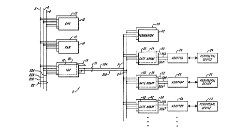
Figure 1 depicts a digital data processing
system 5 having a fault tolerant peripheral
5 input/output system constructed according to a
preferred practice of the inYention. The system 5
includes partnered central processing units 10, 12,
partnered random access memory unites 14~ 16, and
partnered input/output ~ontrollers 1~, 20, connected
10 for communications over system bus 22.
The i/o controllers 18, 20, which are
coupled via flash bus 19, control the transfer of
information and control signals between the system
backplane, represented by system bus 22, and one or
15 more peripheral devices 24, 26, 28. These peripheral
devices can include permanent storage media, e.g.,
disk and tape drives, communications controllers,
network interfaces, and the like.
Peripheral device control and information
20 signal transfers occur over peripheral bus 30, which
includes dual input/output buses 30A, 30B. Signals
carried over these buses are routed to the peripheral
devices 24, 26, 28 via gate arrays 32, 34, 36, 38,
40, 4~ and adaptors 44, 46, 48. As shown in the
25 illustration, each peripheral device, e.g., device
24, is associated with a gate array pair, e.g.,
arrays 32, 34, and an adaptor, e.g., adaptor 44. The
paired gate arrays, e.g., arrays 32~ 34, are
interconnected by a communications line, as
30 illustrated; a.g., see line 50. Moreover, each gate
array is connected to its associated adaptor by an
adaptor bus; see lines 56A, 56B, 58A, 58B, 60~, 60B.
In turn, the adaptors 44, 46, 48 are coupled to their
:
- 16 - 1 3 2 3 4 4 1
respective associated peripheral devices 24, 26, 28
via local peripheral lines, as illustrated.
The peripheral bus 30 and, particularly,
first and second i~o buses 30A, 30B, are terminated
5 by terminators 62, 64.
The illustrated central proces~ing unit~ 10, 12,
the random access memory units, and the system bu~ 22 are
constructed according to the teachings of Canadian patent
Nos. 1,178,374; 1,178,712; and 1,180,453; th~ aforem~ntioned
~P0 patent application, to wit, EP0 Appllcation No. 87 30
7179.9; and United States patents, to wit, United S~ates
Patent Nos. 4,453,215; 4,597,084; and 4,816,990.
According to a preferred practice, i/o buses
30A and 30B serve as redundant signal carriers. That
is, the buses 30A, 30B carry duplicative information
signals synchronously and simultaneously. This
arrangement facilitates the detection of transmission
2Q faults and permits the system to provide continuous,
uninterrupted, processing and communication over the
non-faulty bus.
According to a preerred practice, each bus
30A, 30b, includes data, control, parity, strobe, and
25 ~wait~ signal conductors. Physically, the bus 30 can
be implemented using two cables of 30 twisted pairs
each. Such an implementation permits redundant 8-bit
transfers at 4 megahertz using one cable or,
alternatively, redundan~ 16-bit transfers at 4
~0 megahertz using both cabl~s. Information transfers
alonq bus 30 occur at a cycle rate of 250
nanoseconds, thus providing 8-bit transfers at four
.
' ' ' ,
- 17 - 1323~4~
megabytes per second and 16-bit transfers at eiyht
megabytes per second.
The data, control, parity and wait signal
lines of each i/o bus 30A, 30B are open collector
5 conductors and are driven, for e~ample, by Motorola
26S10 transceivers. Two strobe lines are provided in
each bus 30A, ~OB. These paired lines serve as a
differential signal carriers driven at the i~o
controller 1~, 20 and received a~ terminators 62, 64.
The gate array pairs, which may reside on a
single board, are inserted in slots of an adaptor
chassis (not shown). Each slot is associated with a
slot-id which defines the address of the associated
peripheral device. In one embodiment, the chassis
lS maintains sixteen such addressable slots, with the
far end terminators 62, 64 occupying the final two
slots.
Figure 2 depicts an i/o controller 18
constructed in accord with a preferred practice o
20 the invention. The i/o controller 18 includes a
peripheral bus interface section 18A, a first
processing sections 188, a second processing section
18C, and a system bus interface section 18D. The
peripheral bus interface section 18A provides an
25 interface for receiving, transmitting, and checking
information transfers between the i/o controller 18
and devices attached to first and second i/o buses
30A, 30B. The system`bus interface section 18D
provides interface for receiving, transmittin~, and
3~ chec~ing information transfers between the i~o
controller 18 and those unctional units ~e.g.,
central processing units 10, 12 and random access
memory units 14, 16) attached along the system bus
~2. The first and second processing sections 18B,
- 18 - 1323~41
18C serYe as redundant processing for signals
received by the ;/o controller from system and
peripheral buses.
The per;pheral bus control section 18A is
5 composed o~ two duplicative in~erface sections: the
"drive~ section shown in the upper-left portion of
Figure 2; and the ~check~ section shown in the
lower-left portion of Figure 2. The drive section is
primarily associated with both the first i~o bus 30A
10 ~hereinafter referred to as ~he ~P bus~ and the
first processing section 18B. That is, in the
absence of fault, the drive section couples the P Bus
30A with the first processing section 18B.
Similarly, the check section is primarily associated
15 with the second i~o bus 30B (hereinafter referred to
as the "Q bus~) and the second processing section 18C.
With particular reference to Figùre 2, it is
seen that the drive section of the peripheral bus
interface 18A includes transceiver 66A, input data
20 multiplexor 68A, output data multiplesor 70A,
peripheral bus interface control 72A, function code
loop-back comparator 74A, data loop-back comparator
76A, and peripheral scanner 78A.
Transceiver 66A receives incoming data from
25 the P bus and makes this data available to the
controller 18 on line 82A. The transceiver also
monitors function code signals on the P bus, via line
80A, for loopback comparison. Data generated for
output by the controller 18 is passed to the
30 transceiver via line 86A for transmission along the
bus, while ~unction codes generated for output by the
controller 18 are passed to 66A via line 84A for
transmission along the P bus.
'
.
.. . . . . .
''' ' . ' ' ,- :
. . : . , ~ . .
. . .
- 19 1 32344 1
Incoming drive section data signals are
routed to multiple~or 68A, along with data signals
received from the check section transceiver 66B, as
shown. Data selected by multiple~or 68A is routed
5 along line 90A to the first processing section data
bus 92A.
In the absence of fault, as where duplicate
data signals are received from P bus and Q bus
synchronously and simultaneously, the multiplexor 68A
10 will select P bus data signals, received along line
82A, for routing to irst processing section data bus
92A. However, if the P bus data is detected as
faulty, the multiple~or will select Q bus data
signals, rece;ved alonq line 82B, for routing to the
15 first processing section data bus 92A.
Outgoing data signals generated by the
scanner 78A, the first processing data bus 92A, and
the first processing address bus 94A, are routed
through output multiplexor 70A, which acts under the
20 control of controller 72A. Signals from the
multiple~or 70A are transmitted to the P bus via line
86A, while simultaneously being routed to loop-back
comparator 7SA.
~ The bus interface control 72A generates a
25 function code signal along line 84A for output by the
transceiver 66A. This function code signal is also
routed to the check section for output alonq the Q
bus via line 84B and transceiver 66B. Function code
slqnals generated by control 72A are compared with
~0 incom;ng function code signals, routed on line 80A,
by loop-back comparator 74A.
As shown in Figure 2, the check side of the
peripheral bus interface section 18A is of æimilar
constru~tîon to the drive side o~:that section.
~ : '
"
B
.. , , . :- '
. - ,: . .
.
.. . :
. .
- 20 - 1323441
Accordingly, operation of the check side of the
peripheral bus interface section 18A will be
understood by reference to the discussion above.
With further reference to Figure 2, the
5 peripheral bus interface 18A is seen to include
function code comparator 96. This comparator
compares function code signals produced by both the
drive side interface control 72A and the check side
interface control 72B to produce a siqnal indicating
10 whether these match. The interface 18A further
includes output data comparator 98 and input data
comparator 100. The output data comparator 98 is
arranged for comparing data siqnals selected by the
drive side multiplexor 70A with those selected by
15 check side multiple~or 70B, while the input data
comparator is arranged for comparing data selected by
multiplexor 68A with that selected by check side
multiplesor 688.
In addition to the drive and check sides,
20 discussed above, the peripheral bus interface section
18A includes circuitry for tran mitting local data
and operational status signals to partner controller
20. This circuitry, termed Uflashu circuitry, also
compares data and status signals received from the
25 partner controller 20.
According to the illustrated embodiment, the
flash circuitry includes transceiver 102, comparator
104, and strobe generator 106. The transceiver 102
transmits data signals from the drive side o the
30 interface 18A to the flash bus 19. The transceiver
also transmits operational status signals to the
flash bus 19, as indicated by the signal line denoted
~Y STATE. Data received from the flash bus is
transferred from the transceiver 102 to the
;:
' ' ' ' ' ' ~ ' "
'' ' . ': ' ,
. . , : -
: . . . ':
.,' ' , ' ' ' ' '
- 21 - 1323441
comparator 104, as shown. There, the data i~
compared with check side data routed on line 90B.
State information received ~rom the flash bus is
passed along line 108 to strobe generator 106. If
5 this information compares favorably with local
operational status signals~ or if it is determined
that strobe signals must otherwise be generated,
e.g., during an error detection sequence, the strobe
generator 106 generates strobe information for
10 routing to the P and Q buses via lines 110, 88A, and
88B.
With further reference to Figure 2, the
first processing section 18B includes processor 112A,
timer 116A, EEPROM 118A, map section 120A, and
15 control 1~2A. As indicated in the illustration, each
of these elements is coupled to the data bus 92A for
transmi~ting and recaiving data signals, while the
later four of the elements are coupled to the address
bus 94A for receiving addressing signals. The
20 proc~ssor 112A is arranged for driving addressing
signals onto the address bus 94A.
Interrupt signals generated by the scanner
78A, the timer 116A, and the control 122A are
transferred via line 124A to the processor.
25 Similarly, an error signal designated BER~ generated
by the map section is transferred via line 126A to
the processor ll~A.
The second processing section l~C is
constructed similarly to the first processing section
30 18B, as shown in the drawing.
The controller 18 also includes circuitry
which is shared by the first and second processing
sections 18B, 18C. To wit, a random access memory
module 128 accepts addressinq information from both
.
': '
., ~ , .
'` . .
. ' '. ~ " '
- 22 - 1323~41
address buses 94A, 94B, as illustrated. The module
is also connected ~or receiving and transmitting data
to and from the local data buses 92A, 92B, as shown
in the illustration. The illustration also depicts
5 the transfer o~ paging in~ormation to the memory
module 1~8 from map sections 120A, 120B.
According to a preferred embodiment, data
comparators 130, 132 monitor signals received from
the local data buses 92A, 92B to identify
10 discrepancies between ~hem. A further csmparator 134
monitors signals received from the local address
buses 94A, 94B, as well as signals generated by map
sections 120A, 120B, to identify differences
therebetween.
The system bus interface section 18D
includes address multiplexor 136, data multiple~or
138, as well as standard interface control 140. The
address multiplexor 136 transfers output address
signals f rom the map section 120A and the address bus
20 94A to the system bus 22 and, more particularly, to
the duplicative buses 22A and 22B. The data
multiplexor 138 transfers output data signals from
the local data bus 92A ~o the duplicative buses 22A
and 22B, as shown in the illustration. As further
~5 depicted in Figure ~, address and control information
received by the address and data multiple~ors 136,
138 is routed ~o ~he standard inter4ace co~trol 140.
From there, this incoming information may be routed
via line 142 to controls 122A and 122B.
B
.
.
,
.
- 23 - 1323~41
I/O ~Qntrol~er P~ripheral 8us Inter~2~
According to one preferred practice, i/o
controller 18 can be connected with the peripheral
bus 30, via transceivers ~6A, 66B, to send and/or
5 receive the signal~ identified below~ Hereina~ter,
the i/o controller is referred to as the ~IOP~, while
a gate array/adaptor combination, e.g., gate array~
32, 3~ and adaptor 44, is referred to as an
~interfacsn or UIOAW.
10 Signal Name Description Si~nal Directi~n
Data 0 P Bus P Data Bit O IOP to~from IOA
Data 1 P Bus P Data Bit 1 IOP to/from IOA
Data 2 P Bus P Data Bit 2 IOP to/from IOA
15 Data 3 P Bus P Data Bit 3 IOP to/from IOA
Data 4 P Bus P Data Bit 4 IOP to~from IOA
Data 5 P Bus P Data Bit 5 IOP to/from IOA
Data 6 P Bus P Data Bit 6 IQP to/from IOA
Data 7 P Bus P Data 8it 7 IOP toffrom IOA
20 Da~a Parity P Bus P Data Parity IOP to/from IOA
Data 0 Q Bus Q Data Bit O IOP to/from IOA
Data 1 Q Bus Q Data Bit 1 IOP toffrom IOA
Data 2 Q Bus Q Data Bit 2 IOP to/from IOA
25 Data 3 Q ` Bus Q Data Bit 3 IOP to/from IOA
Data 4 Q Bus Q Data Bit 4 IOP to/from IOA
Data 5 Q Bus Q Data Bit 5 IOP to/rom IOA
Data 6 Q Bus Q Data Bit 6 IOP to/from IOA
Data 7 Q Bus Q Data Bit 7 IOP to~from IOA
30 Data Parity Q Bus Q Data Parity IOP to~from IOA
Func 0 P Bus P Function Code IOP to IOA
Bit 0
Func 1 P Bus P Function Code IOP to IOA
Bit 1
Func 2 P Bus P Function Code IOP to IOA
Bit 2
Func Pari~y P BuS P Function Code IOP to I~A
Parity
Func 0 Q Bus Q Function Code IOP tC IO~
~ Bit 0
Func 1 Q Bus Q Function Code IOP to IOA
Bit 1
1~
.
,
:, ,
:
- 24 1 323~ 4 1
Sianal Nam~ DescriptiQn Siqnal Dir~ction
Func 2 Q Bus Q Function Code IO~ to IOA
Bit 2
5 Func Parity Q Bus A Function Code IOP to IOA
Parity
Strobe P Bus P Strobe IOP to IOA
positive conductor
of differential
pair
Stro~e P~ Bus P Strobe IOP to IOA
negative conductor
of differential
pair
Strobe Q Bus Q Strobe IOP to IOA
positive conductor
of differential
pair
Strobe Q* Bus Q Strobe IOP to IOA
negative conductor
o differential
pair
Wait P Bus P Wait IOA to IOP
Wait Q Bus Q Wait IOA to IOP
According to a preferred practice, i/o
30 controller 18 transmits and receives on the flash bus
19 the signals listed below, wherein the first i/o
controller, e.g., controll~r 18, is referred to as
~IOP ln, and the second i/o controller, e.g.,
controller 20, is referred to as UIOP 2~. ~n ~n in
35 the signal name indicates that the signal is
inverted. The flash bus 19 is a wire OR'ed
open-collector. The controllers IOP 1 and IOP 2
concurrently present a signal level on the bus 19,
with th~ ~low~ level prevailing and being received by
40 both controllers.
Siqnal Name PescriPtion Si~nal Direction
FDATA Q* Flash Bus Data Bit 0 IOP 1 to/from
IOP 2
1 32344~
- 25 - - .
Siqnal Name DescriPtiOn Siqnal Dire~tion
FDATA 1~ Flash Bus Data Bit 1 IOP 1 to/from
IOP 2
5 FDATA 2* Flash Bus Data Bit 2 IOP 1 to~from
IOP 2
FDATA 3~ Flash Bus Data Bit 3 IOP 1 to/from
IOP 2
FDATA 4~ Flash Bus Data Bit 4 IOP 1 to/from
IOP 2
FDATA 5* Flash Bus Data Bit 5 IOP 1 to~from
IOP 2
FDATA 6* Flash Bus Data Bit 6 IOP 1 to~from
IOP 2
15 FDATA 7* Flash Bus Data Bit 7 IOP 1 to~from
IOP ~
WE STRB* IOP to iSSU8 STROBE IOP 1 to/from
IOP 2
20 WE HOLD STRB* IOP to hold STROBE IOP 1 to/from
because of WAIT IOP 2
CF NEQ* Check side data does IOP 1 to/from
not equal flash data IOP 2
CD NE~* Check side data does IVP 1 to/rom
not equal drive side IOP 2
data
P NOK* Failure detected in IOP 1 to/from
Bus P IOP 2
Q NOK~ Failure detected in IOP 1 to~from
Bus Q IOP 2
Memory Allocation
The i/o controller 1~ and its circuitry is
35 allocated in a virtual memory configuration as
follows:
Addres~ Content
000000~ - BDFFFFx User mapped virtual memory
40 BE0000x - BEFFFF~ PROM ~elements 118A~ 1188)
also residing at 000000~ -
00ffff~ when PROM is not high
BF0000~ - BF7FFF~ Not used
BF8000~ - BF8FFF~ Sync paga
45 BF9000~ - BF9FFF~ P Bus DMA (direct memory
access~ ~elect~P Bus command
.pa~e
.
- 26 - 1 32 34
Address Content
BFAOOO~ - BFAFFF~ Supervisor control (incl.
control registers for P bus
timer ~lements 116A 116B)
scanner (elemen~s 7~A 78B and
scanner list)
BFBOOO~ - BFBFFF~ Privileqed control
BFCOOQx - BFFFFF$ Map (elements 120A 120B~
10 COOOOOs - FFFFFF~ P Bus programmed i/o space
providing a 4 MByte window into
the selected adaptor
Within the DMA select~interface command
15 page address space is arran~ed as follows:
BF9002X write word Select Adaptor for PIO
command
Bits 15-08 Slot~subchannel
07 ~1~
06-00 Command number
BF9004-006 write long Selsct peripheral adaptor
for DMA write
Bits 31-24 Slot/subchannel
23-22 ~0~
21-16 Upper sis
adaptor address
bits
15-00 Lower sixteen
adaptor address
bits
35 BF9008- write long Select peripheral adaptor
BF9OOA for DMA read
Bits 31-24 Slot~subchannel
23-22 00
21-16 Upper si~
~o adaptor address
~its
15-00 Lower sixteen
adaptor address
bits
BF9OOC write long ~elect Adaptor for DMA
Verify
Bits 31-24 slot/subchannel
23-22 ~00~ ~
~B : ; ~
- 27 - ~323~1
Addre~s A~cess Conten~
21-16 up 6 peripheral
adaptor address
bits
15-00 lower 16
adaptor address
bits
10 Supervisory Control Pane
Supervisory control page accesses are mad~
at virtual page BFA000~. The timer, peripheral bus
and scanner control, including the scanner list, are
addressed in this page. USER and CODE accesses to
15 this page cause the generation of BERR* along line
126A. The page also maintains selected interrupt,
privilege, and scanner interrupt status information.
All control accesses to the supervisory
control page, except for accesses to timer 116A
20 require no wait states. Unlatched control pulses are
initiated by the rising edge of a first timing signal
and terminated by the falling edge of a subsequent
timing signal. Control bits for the standard bus
interface and P bus are synchronized to a 4 MHz clock
25 signal.
Within the ~upervisory control command page,
i~o address space is allocated as follows:
Addres~ Ac~ess Content
30 BFA000 Read Timer Data Word
BFA002 Timer Status Word
Bits 15-00
BF~000 Write Timer Data Word
35 BFA00~ Timer Command/Data
Poin~er Words
Bit8 15-00
~FAioo Read Checksum Word
~its lS-00
'
B
- 28 - ~323~
Address Acc~~ Cont~a~
BFA400 Write PUBS/SCANNER/DEV CONTROL
WORD
Bit 15 (1 to set/0 to
clear)
Bits 02-01-00
1 1 1 PBUS Enable Bit
(active hi~
1 1 0 Set ~BUS-BERR
Enable Bit
(active hi)
1 0 1 Scanner on
~active hi3
1 0 0 Run Scanner
~active hi)
0 1 1 Timer Interrupt
Mask/Clear
~mas~ed off lo)
0 1 0 Level 1
Interrupt
(active hi)
0 0 1 Privileged Bit
(active low)
0 0 0 PBUS Lock
(actiYe low)
BFA800 Read Scanner Interrupt Status
Word (to be read only if
a scanner interrupt is
pending)
Bits 15-00
Bit 15 Adaptor Alive
(active hi)
Bit 14 Adaptor Interrupt
(acti~e hi)
Bit 13 Adaptor Obeying P
Bit 12 Adaptor Obeyinq Q
~its 11-8 Adaptor
Interrupt Code or
Subchannel
Bits 7-4 Slot number
Bits 3-0 TBD (subchann~l)
BFA801 write PTO Slot Select Address
Byte
Bits 7-4 Slot number
Bits 3-0 TBD ~subchannel)
B~
1 3234~ 1
AddrQss Accçsfi ÇQn~çn~
BEAC01- Read (Odd Scanner Slot Select
BFADFF Addresses) Address Byte
Bits 7-4 Slot number
Bits 3-0 TBD (subchannel
BFAC01- write (Odd Scanner Slot Select
BFADFF Addresses) Address Byte
Bits 7-4 Slot number
Bits 3-0 TBD (subchannel)
Privileqe Control Pag~
Privilege control page accesses are made at
15 virtual address BFB000~. The controller 18
privileged-only status and control registers are
stored in this virtual page. Additionally, the
standard bus interface 122A control resides in this
page. Accesses to the privilege control page require
20 no wait states.
Within the privileged control page, i/o address
space is arranged as follows:
Ad~ress Acç~ Content
25 B~B000 Read Board Status Word (note:
if one, a mask bit allows
the interrupt for the
specified condition)
Bit 15 BROKEN
Bit 14 BROKEN TWO
Bit 13 MEMORY BROXEN --
Parity~Data
Bit 12 MEMORY BROKEN --
Compare
Bit 11 TIMER INTERRUPT MASK
5enabled if 1)
Bit 10 P~ COMPARE tHi=OK)
Bit 0~ COMMAND PENDING
Bit 08 STATUS CHANGE
Bit 07 Side C - 1, D ~ PROM
HI -- read only
Bit 06 INTERRUPT PENDING
tfrom IOP on Strata-BUS)
Bit 05 PARTNERED bit
Bit 04 ZO~T G~
: ;
::
- -
,
.
.. : . . :
_ 30 - 13~3~4~
Addres~ ~ç~ Con~en~
B;t 03 LEVELl INT
Bit 02 P~OM HI -- when this
b;t is cleared, PROM
addresses start at 0 and
RAM addresses below R000
are not available.
When prom ;s high, Side D
is also high. When prom is
not high, ~ide iS low.
Bit 01 INTERRUPT MASK for
Bit 09 ~CMD PENDIN~ being
1 (Level 4)
Bit 00 INTERRUPT MASK for
all conditions and levels
~Bits 00-05 are 0 after a
RESET.)
BFB000 Write Board ~tatus Word
Bit 15 (1 to set~0 to clear)
Bits 02-01-00
1 1 1 P PBUS Enabled
1 1 0 Q PBUS Enabled
1 0 1 PARTNERED bit
1 0 0 OUTPUT GRANT bit
0 1 1 PBUS OBE~ FORCE
bit
0 1 0 PROM HI bit
O O 1 INTER~UPT MASK
for ~CMD PENDING)
Level 4
O O O INTERRUPT MASR
~or all
conditions and
levels
BF~401 Read Standard Interface Command
Register Bytes
BFB403
BFB405 Bits 07-00 for all
BFB407
45 BFB400 write Board Control Word
Bits 15--02-01-00
0 1 1 1 CLEAR BROKEN
~only used ~y
PROM code):
'
' ~
- 31 - 1323~41
Ad~r~ss Access Content
O 1 1 0 CLEAR BROKEN TWO,
CLEAR MEMORY,
PARITY ERROR,
CLEAR MEMORY
COMPARE ERROR,
CLEAR INTERRUPT
LEVELS 2-3, CLEAR
PR COMPARE ERROR,
CLEAR
W~IT-TIMEOUT
ERROR~ CLEAR PBUS
OBEY ERROR
~5 0 1 0 1 CLEAR CHECRS~M
O 1 0 0 SYNC JIFFY TIMER
0 0 l l SET INTERRVPT
REQUEST
O O 1 0 CLEAR DMA ENABLE
0 O O 1 CLEAR COMMAND
PENDING
0 0 0 0 CLEAR ~TATUS
C~ANGE
25 BFB801 Read Sta~dard Interface Pointer
Register Byte~
BF8803
BFB805 BitS 07-00 for all
BFB807
BFB80l Write Standard Interface VOS
Vector Byte
Bits 07-00 Vector *umber
35 BFBC00 Read P~us Status Word
Bit 15 VERIFY OK
Bit 14 DMA WRITE
Bit 13 DMA REA~
Bit l2 SCANNER:INTERRUPT
(active low)
Bit }1 ~CANNER SET TO RU~
(active low)
Bit 10 PBUS OBEY FORCED
Bit 9 P PBUS ENABLED Sync
Bit 8:~ PBUS ENABLED Sync
~it 7 PBUS WAIT-TIMEOUT
ERROR (active low)
Bit 6 PBU~ OBEY ERROR
(active low)
:: :
::
~ :; : :~ '
.
.,
,,
- - , -
- 32 - ~ 3234 4 1
Adç!res~ Access Content
Bit 5 PBUS SELECT ERROR
~active low)
Bit 4 PBUS SELECT BERR
ENABLED (active hi)
Bit 3 PBUS ENABLED Sync
Bit 2 PBUS LOC~ (locked if
low)
Bit 1 OBEY P
Bit 0 OBEY Q
BFBC00 Write CHECKSUM TEST WORD/BYTE
Bits 15 8 Add byte ~if
asserted) to checksum ~or
t~st
Bits 7-0 Add byt2 tif
asserted) to checksum for
test
The Map Element
In a preferred embodiment, the map 120A
includes four pages of ~4 bit map entries, each
25 having sixteen physical address translation bits, one
i/o bit, one interlock bit, three access control
bits, one local/main memory bit, one DMA thread bit,
and one spare bit. The translation addres~ bits are
aligned on even word boundaries, while the control
30 bits occupy a bytes aligned on odd word boundaries.
The access control bits are allocated to define the
following access types:
no access;
any access - write only memory;
any access - read data~e~ecute;
any access - read data/write data;
privileged access - no access;
pri~ileged access - write:only memory;
privileged access - read data~e~ecute;:and
privileged access - read:data~write data.
According to one preferred embodiment, the
following memory access control violations:will cau~
assertion of BERR~ on line 126A~
: ' -
. ., ~, ~ .
, ' :. ~ -, :
- 33 - 1 3~3~ 4 1
1) an unprivileged access to a privileged
page;
2) an e~ecute acce~s to a write accessible
page:
33 a write access to a non-write
accessible page; and
43 a read access to a non-read accessible
page.
Moreover, the following local virtual access
violations can also cause assertion of ~E~R, as above:
1) a code access to the local virtual
pages, e~cept prom 118A;
2) an unprivileqed write access to the
privileged control page;
3) a user access to the supervisor c~ntrol
page;
4) a write to prom 118A;
5) an overrange during local memory access;
S) a read to the sync selection page;
7) a peripheral bus time-out error
occurring during a peripheral bus
access;
8) a peripheral bus obey error occurring
during a non-DMA peripheral bus access,
except when bus obey is forced;
9) a peripheral bus obey error occurring
during a DMA cycle; and
10) a CPU ~112A) write during a DMA cycle.
In the illustrated embodiment, a peripheral
bus select error will be generated under the
following circumstances:!
1) a peripheral bus access to an empty or
broken peripheral bus device adaptor
slo~ in the adaptor chassis, except
when peripheral bus select errors are
di~ables;
2) a peripheral bus DMA with either
addressing bit 1 or data bit 7 asserted;
3) a peripheral bus command with address
bit 1 de-asserted:
4) a peripheral bus select when the
peripheral bus is defined as locked;
45 ` 5) a peripheral bus access when the
peripheral bus is turned ~f.
B
- . - . . :
.
. .
.
_ 34 1 3~34 4 1
Local Memory Acces~
The illu~trated controller 18 utilizes a 12
Motorola 68010 processor 112A which e2ecutes
instructions out of local memory 12~ with no wait
5 states, unless a memory refresh is demanded.
With regard to operation of t~e memory 128,
a row strobe signal RRAS* is issued on every cycle of
the local processor 112A. If the cycle is a local
memory access, and (i~ a refresh ~s not demanded,
10 and (ii) a LOCAL VIRTUAh or an IACK cycle is not
decoded, strobe signal RCAS* will be issued;
otherwise, RRAS* ABORT will be issued, thereby
terminating RRAS*.
Terminating RRAS* allows a free refresh to
15 occur, so long as a refresh is requested after the
signal AS~ is asserted during a CPU bus cycle having
3 or more wait states. It is necessary to be able to
perform a refresh while AS* is asserted so that
during synchronization of partnered i/o controllers
23 18, 20, mem~y refresh ~imes are not violated while
the local CPU 112A is waiting, with AS* asserted, for
the other board to catch up.
Most refresh cycles occur by demand, i.e.,
the refresh cycle begins before AS~ is asserted,
25 regardless of the type of the next cycle. If the
next cycle is a local memory access, the refresh
cycle will add 3 wait states; otherwise, no wait
states will be added.
A signal R~S PRECHARGE* is clocked by the
30 rising edge of RRAS* to prevent any reassertion of
RRAS*. Assertion of RAS PRECHARGE* also prevents a
refresh cycle from occurring before the RAM has had
time ~o recover from a RAN access abort or a lat~
negation of AS*.
B
.
1 32344 1
Addresses to the RAMs are selected by a
signal SELCOL~, which follows R~AS* by 1~ nsec. Row
addresses to the RAMs are the low order address bits
of the CPU 112A and do not have a map translation
5 delay. Some of the column addresses are part of the
mappea address area and have map translation delay.
The first processing section 18B employs a Motorola
74F~21 to determine whether the local memory acces~
being made is within the range of the local memory
10 space. If not, the signal OVE~RANGE is asserted.
A refresh cycle occurs synchronously with
the 12MHz clock signal. A refresh request is
generated as a result of the falling edge of timer
clock, which is synchronized to the rising edge of
15 tha 12MHz CLK, every 15.25 microseconds.
Map Access
Access to map unit 120 occurs with no wait
states. The map 120A, when used for address
20 translation, is 4K lonq by 2~ bits wide, including 16
physical address bits and eight control bits. Map
entries reside on word or long word boundaries, with
byte acce~ses being unallowabls. Even addressed
words store the 16 bits of translation information.
25 The upper eight bits o~ the odd addresse~ word are
the control bits, including read access, write
access, privileged access, local memory, interlock,
ifo, dma, and spare bit signals. The lower eight
bits of the odd-address words are not use.
The map 120A virtual page access are
privileged only/data only access; an unprivileged or
codè access will cause BERR~ to be asserted. These
pages are also write protected from the unprivileged
access.
.. - ~ ~ ';
. . . ~ . -.
:, .
- 36 - 132~3
Time~
The timer 116A, including its associated
jiffy counters, is synchronized with the 12 MH2 clock
signal. The timer has a period of 15.25 microseconds
5 which is asserted for 1.3 microseconds and ~nasserted
for 13.9 microseconds. Timer signals are
re-synchronized ~o the 12 MH~ CLX after the counters
reach ~ selected value, A signal, TIMER STABLE*, is
negated 1.3 microseconds before the rising edge of
10 the timer clock si~nal, while being asserted 1.3
microseconds after that risinq edge to prevent
accessing the TIMER too close to its clock edge. The
timer 116A addresses are ~tored within the
supervisory control virtual page as noted above. The
15 timer 116A may only be accessed at word boundaries.
Such accesses add from 1 to 31 wait states to the CPU
112A bus cycle depending on the state of a signal
TIMER* STABLE when the access is made. For the timer
116A ~o interrupt the processor 112A, the interrupt
20 mas~ TIMER IMSK must be set to one. Upon servicing a
TIMER IN~ERRUPT, TIMER IMSK must be set to zero to
clear the condition, and then set to one to re-enable
interrupts from the TIMER.
25 Interr~t A~knowle~gç
The processor 118A provides an interrupt
acknowledge cycle, IACK, requiring no wait states.
On any interrupt acknowledge, the lower three address
bits on local address buses 92A, 923 indi~ate which
30 level interrupt the process is servicing. Thes~
three b;ts ars returned to the processor in an
interrupt vector byte, with the high order bit of the
byte as asserted. The interrupt levels are as
follows. ~ -
~3 ' ;
,. ~
, ~ : , ~ :
37 1 32344 1
Interrupt Level Device
LEVEL 7 DEBUGGER
LEYEL 6 TIMER
LEYEL 5 SCANNER
LEVEL 4 CMD PENDING
LEVEL 3 PBUS TIME OUT or OBEY ERROR
LEVEL 2 PBUS OBEY TOGGLE CLOCX
LEVEL 1 S~FTWARE ~NTERRUPT
Scanner
The illustrated scanner 78A runs as a
parallel processor to the main board CPU. If enabled
and set to run, it will scan the adaptors in th~
15 adaptor chassis in a software assignable order for
interrupts and lack of alive status. The scanner
takes advantaqe of the select mechanism o the
adaptors by using an aborted select to retrieve
adaptor status. This allows a 750 nanosecond scan
20 cycle for each entry in the scan list.
A scanner table entry is one byte long,
including four bits designating a peripheral slot
number and four bits desiqnating a subchannel number.
The software controlled scan list forces the
25 scanner 78A to check only those slots which are
occupied. The scanner may be utilized to compensate
for different interrupt service requirements of
different adaptors by including selected adaptor
slots more than once in the scan list. The scan list
30 consists of 256 entries. All entries must be
contiquous, starting at the first entry. However,
the entire scan list does not have to be filled. A
~return to zero~ entry is employed ~y the scanner 78A
to scan the ~ctive terminators in the adaptor
35 chassis. An interrupt ~rom such a scan to the
terminator indicates a bulk power supply failure, fan
`B
.
1 323~1
- 38 -
failure, power synchronization ~ailure, or a
terminator failure.
The scanner i8A, upon finding a slot with
the interrupt bit set or the alive bit cleared, will
5 stop at that entry and interrupt the processor 112A.
When reading back the scanner interrupt status word,
the processor 112A reads the adaptor status in one
byte and the contents of the scan list entry in the
other. The scanner interrupt status i8 not read
10 unless there is an interrupt or the scanner is not
set to run.
The scanner 78A runs when it is enabled and
there are no processor 112A pending on the peripheral
bus 30. The processor 112A cycles have priority;
15 accordinqly, the scanner 74A will stop while during
those cycles and restart only after the first idle
cycle during which the processor 112A does not access
the bus. The scanner 78~ stops completely when an
adaptor is selected for DMA and restarts when DMA
20 enable is cleared.
Flash Circuitry
Figure 3 depicts a preferred construct;on
for the flash circuitry of an i~o controller 18. The
25 circuitry includes AND gates 142A, 142B, 142C, 142D,
NOR qates 144A, 144B, 144C, inverters 146A, 146B,
NAND gates 148, NAND gatP 150, OR gate 15~, and
buffer 154. The flash circuitry provides, as output
from NAND qates 148, controller operational state
30 signals which are OR'ed onto the open collector flash
bus 19.
The AND gates 142A accepts the following
input signals:
~3
- 39 1 3234 4 1
Sianal Desç~iption
PDATA PAR OK D~ validity of data signal
parity at transceiver 66A
PDATA E~ i/o controller enabled to
dr;ve data onto the
peripheral bus 30
OBEY P i~o controller enabled to
send~receive on the P bus
3DA
WAIT IN P i~o controller receiving
WAI~ siqnal on the P bus 30A
FC LB OK P* function code loopback
comparator 74A output
DATA LB OK P* data loopback compaxator
76A output
PDATA EN D i~o controller drive side
18B enabled to drive data
onto peripheral bus 30
Logical AND's of the above signals are
generated by AND gates 142A in the manner indicated
in the illustration. Outputs of the array 142a are
passed to NOR gate 144a to produce a binary signal,
25 MX P NOK~, representative of the validity of
information transfer signals received from the P bus
30A. In particular, NY P NOX* has an assertive state
indicating that signals received from the P bus by
the i/o controller, e.g., controller 18, contain
30 errors. While, MY P NOK* has a non-assertive state
indicating that no obvious fault has occurred in the
signals received from the P bus. The æignal MY P
NOX* is routed through inverter 146a~
In a similar manner, the AND gates 142b and
35 NO~ gate 144b produce a binary signal, MY Q NOR~, :
representative o the validity of information
transfer siynals received:Prom the Q bus~30B. The ; : -
signal MY Q NOK~ is routed through inverter 146b.~ ~
The A~D gates 142C, 142D~and NOR ~GATE 144C ~:
40 are arranged to generate an I WAIT* signal~, having~an
: : :
:
~, ~
-. , : . . . , ~
'
. :, ', "'- ''
40 - ~ 32344 ~
assertive state indicating that the controller i~ to
delay generation of the strobe signal.
The NAND gate 150 is arranged to generate a
binary signal, PK ONLINE*, as a boolean NA~D o the
5 following input signals: ~
~ignal Descr~ption
BROXEN BUF*
PK COMARE
PBUS ENS D : ` `
The PR ONLINE* signal, which has an
assertive state indicatiny that the associated i~o
controller is online, is negated by negated-input OR
15 gate 152, as shown. The resulting signal PK ONLINE
is tied through resistor 156 to potential IVCC and,
further, is coupled to an input of each of the ~AND
gates in array 148. The output of gate 152 is also
retained in bufer 154 to provide the buffered signal ` ``
20 BUF PK ONLINE.
With further referenc~ to Figure 3, outputs
of each of inverters 146a and 146b, as well as each
of the signals listed below, is provided a~ a second
input to individual NAND gates in array 148.
Signal Description
MY CD EQ* output of compar2tor 100
MY FLASH EQ~ output of comparator 1~4
STRB HOLD D drive side of iJo
controller delaying strobe
signal generation
STRB ~OLD C check side o i~o
contrQller delaying strobe
signal generation
~S STR08E D drive side regenerate of
strobe
STROBE C check side regenerate of
strobe
B
.
.. . . : .
. . .
.
- 41 - 1323441
The output of the NAND gates of array 14~
are passed to the open collector conductors of flash
bus 19 as shown in the illustration.
5 Strobe Si~nal ~enera~iQn
Figure 4 depicts one preferred configuration
of circuitry used to generate pre-STROBE signals in
i/o controller 18, 20. The illustrated circuitry
includes counter 158, flip-flops 160, 162, 164, 166,
10 NAND gates 167, 168, 170, 172, OR gatss 174, 176,
178, NOR gate 180, and ~uffers 18~, 184.
The counter 158 is driven by a 1 MHz clock
signal provided in the drive side of the i/o
controller. A clear input to the counter 158 is
15 provided by the output of NAND gate 167, having at
its negated inputs, a WE HOLD STROBE* signals and a
timing signal, desiynated T5 D~. ThP fourth output
bit of the timer 158 is coupled to ~D~ input of
flip-flop 162, as shown.
The flip-flop 16~ is arranged for generating
a WAIT TO signal, reflecting that a time out is
re~uired in order to permit error chec~ing. As shown
in the illustrated embodiment a delay of eight
microseconds, resulting from assertion by one or more
25 peripherals of a WAIT signal on the peripheral bus,
causes the aforementioned time out. The negated
output of flip-flop 162 is routed to provide an input
to OR gate 176.
A second input to OR gate 1~6 is provided by
30 the SET STROBE output of NAND gate 168. Inputs to
gate 168 include PNOR*, QNOX, CDNEQ*, WE HOLD STRB~,
PK OK, FDATA CLR D ~an output of the drive sid~ flash
data clock~, FDATA CLK C (an output of the check side
~lash data cloFk~, TO D (the drive side primary
.. . ..
.:
. ~
.. . ' ' .'
.. ..
.
1 32344~
- 42 -
timing signal for the peripheral bus transfer cycle),
T0 C ~the corresponding signal generated on the check
side), WAIT TO*, PBO error ~indicating a bus obey
error~, and BUF PK ONLINE.
The SET STRB* output of N~ND gate 168 is
also provided as the ~ input to flip-flop 16S. A
clear input to that flip-flop is provided as an
output of the gates 170, 172, and 174, as shown in
the illustration. The flip-flop 166 provides as
10 output the ERROR CLK and ERROR CLK~ si~nals, which
provida timing signals for the error sequence
initiated by the i/o processor during the time out.
As shown at the top of Figure 4, a FORCE
STRB~ signal is generated by the combined actions of
15 flip-flop 160 and NOR gate 180. This FORCE STRB~
serves as a preset to 1ip-flop 164, which serves to
generate a STROBE OUT signal at its ~Q~ output. The
clear input to that flip-f lop is provided by a STROBE
CLR* signal. A 16 MHz clock signals g~nerated by the
20 check side drives the flip-flop 164.
As further shown in the illustration, the
STROBE OUT output of flip-flop 164 is retained in
buffers 182 and 18~, providing STROBE D and STROBE C
signals, respectively.
Figure 5A depicts a preferred circuit for
generating a STROBE P signal or transmission along P
bus 30~. The circuit includes a AND gate, having as
its inputs the STROB~ OUT signal ~see Fig. 4) and a
~UF PK ONLINE signal (see Fig. 3~. The output of the
0 AND ~ate 186 is output to the STROBE P pin of the bus
30~ via diode 188, resistors 190a, 190b, 190C, 190d,
and transistor 192, as shown.
Figure 5B depicts a preferred circuit ~or
generating a STROBE P* signal or output along P bus
':
:: ~: :
- .
,
.
~ 323441
- 43 -
30A. The circuit includes an AND gate array l9~a,
194b, 194c, 194d, and inverters 196a, 196b
implemented in combination with resistor 198 as shown
in the illustration.
Figure 6A depicts one preferred
configuration of circuitry utilized in i~o controller
18, 20 for generating an OBEY P si~nal, condition;ng
the controller is to respond only to those peripheral
bus signals received on the first i~o bus 30A. The
10 illustrated circuitry includes OR gate 200, NAND gate
202, and flip-flop 204~
The OR gate 200 produces a TOGGLE P signal
representative of a boolean logic O~ of the P NOX*
signal and the ONE BUS* signal (indicating that the
lS i/o controller is currently conditioned to receive
signals on only one o the i/o bu~es 30A, 30B~. The
TOGGLE P signal is routed to provide the ~j~ and ~k~
inputs to flip-flop 204.
The negated preset signal for flip-flop 204
20 is provided by the FORCE P* s;gnal output of NAND
gate 202. The FORCE P* signal results from the
boolean NAND function of the PK FORCE D signal
(indicating that the i/o controller is conditioned to
respond on the drive side) and the P ENS D signal
25 (indicating that the P bus ;s enabled).
A clock input to flip flop 204 is provided
by a TOGGLE OBEYS* signal, resulting from a boolean
NAND of the ERROR CLK siqnal (see Figure 4) and a PBO
ERROR* signal ~see Figure 7).
The flip-flop 204 provides the
aforementioned OBEY P signal at its ~ output, while
providing the inYerse æignal, OBEY P~, as the negated
ou~put.
`- .~ ' ..
.
1 323~4 1
- 44 -
Figure 6B depicts one preferred
configuration of circuitry utilized in i~o controller
18, 20 for generating an OBEY Q signal, conditioning
the controller is to respond only to those periphersl
5 bus signals received on the sec~nd i~o bus 30B. The
circuit is constructed similarly to that sho~n above
in Figure 6A,
Figure 7 depicts one preferred configuration
of circuitry utilized in i~o controller 18, 20 for
10 generating bus and time-out error signals. The
circuitry includes counter 206, ~ND gate array 208,
NOR gate 210, flip-flops 212, 214, and NOR gates 216,
218.
As shown at the left of the illustration,
15 the clear input of the counter is provided by the TO
D*, the inverse of the drive side 18B TO clock
signal. ~ clock input to the counter 206 is provided
by the ERROR CLK~ signal ~see Figure 4). The second
output bit of counter 206 drives a TOGGLED OUT
20 signal, which serves as an input to A~D gate array
208. The AND gate array 208 also accepts as:input
TOGGLE P ~Figure 6A), TOGGLE Q (Figure 6B), ONE BUS~
~the inverse of a boolean exclusive OR of the OBEY P
and OBEY Q signals), PK FORCE D, PK FORCE D, OBEY P
25 (Figure 6A), OBEY Q (Figure 6B), P NOK~, and Q NOK*
signals.
Output of AND gate array 238 is routed to
NO~ gate 210, as shown in the illustration. This
ga~e produces a SET PBO ERR~ signal, which provides
30 an input to NOR gate 211. As illustrated, a second
input to gate 211 is provided by the non-inverting
output of flip-flop 212. The output of NOR gate 211
drives the ~D~ input of ~lip flop 212, as shown. In
operation, once PBO ERROR* is se~, it is held by the
~3
.
:,, . . ` ~ ,
`
.
.
.
. `
~ 323~ 1
- 45 -
NOR gate 211 until cleared by the CLR MEM ERR~
signal. The clock input for that flip-flop is
provided by the ERROR CLK signal, while the preset is
driven by the CLR MEM ERR~ signal (indicating that
5 the error signal is to be cleared). At its
non-inverting output, the flip flop 212 drives a PBO
ERROR signal, indicating that a peripheral bus error
has occurred.
As further shown in Figure 7, the flip-flop
10 214 has a clock input which is dri~en by the WAIT TO~
signal ~Figure 4), and a clear input driven by the
CLR MEM ERR~ signal. At its invertinq output, the
flip-flop 214 drives a TO ERR~ signal, indicating
that a time-out error has occurred.
The PBQ ERROR* and TO ERR* signal are routed
to inverting inputs of NOR gates 216 and 218, as
shown. Output of these gates provide PBUS ERROR D*
and PBUS ERROR C* signals, indicating a peripheral
bus error has been detected in each of the drive and
20 check sections of the ifo controller.
Figure 8 depicts a timing sequence for two
information transfer cycle types -- a command cycle
and a scanner cycle -- e~ecuted by an i~o controller
acting according to a preferred embodiment of the
25 ;nvention. During a scanner cycle, the iio
controller, under control of its scanner units
(Figure 2, elements 124A, 124B), interrogates
paripheral units and their respecti~e interfaces,
i.e., gate arrays and peripheral adaptors, to
30 determine the operational state thereof. In a
command cycle, on the other hand, the i~o controller
sends a one-byte command to a selected peripheral
device.
- 46 - 1 3234 4 1
Referring to Figure 8, wave forms
transmitted on the strobe conductors of each of the
first and second i/o buses, i.e., the STROBE si~nal,
are shown on wave form line 220. Falling edges of
5 the STROBE signal define information transfer timing
intervals, as shown by consecutively numbered time
;ntervals at the top of the illustration. Line 222
represents the content of signals transferred on the
function code conductors of each of the first and
10 second i/o buses, while line 224 represents the
content of signals transferred on the data conductors
of those buses.
As indicated by line 222 in Timing Interval
0, the system is in an idle state, with an IDLE
15 function code being asserted on the i/o bus function
code conductors. Concurrently, as shown by line 224,
all one's are asserted on the data conductors.
In Timing Interval 1, the i/o controller
commences a command cycle. Particularly, the SELECT
20 function code is asserted on the function code
conductors -- see line 222 -- while a peripheral
selection addressing byte is transmitted on the data
conductors -- see line 224. This peripheral
selection addressing byte can include, as in the
25 preferred embodiment, four SLOT ID bits and four
~subchannelN bits. Gate arrays (Figure 1, elements
32, ~ . . . 42) can be conditioned to respond to
selected channel/subchannel bit patterns to determine
whether the command cycle is directed to the gate
30 array, its associated adaptor, and~or its associated
peripheral device.
In Timing Interval 2, the i/o controller
asserts IDLE on the function code conductors o~ the
i/o buses while monitoring the data conductor~ of
. :- :
1 323~ 1
_ 47 -
those buses to receive a response from the addressed
peripheral device or interface. ln absence of fault,
the i/o controller will expect to receive an ALIVE
siqnal -- e.g., an asserted seventh bit in an
5 otherwise non-asserted transmission byte -- on the
data conductors, indicating that the addressed
peripheral is operational. The addressed peripheral
and interface can also respond, during the Timing
Interval 2, with a signal indicating that an
10 interrupt is pending, or with signals indicating
which i/o ~uses are bèing obeyed. Absent error, the
command cycle continues in Timing Interval 3 with the
transmission of a peripheral/interface command
signal. In one embodiment, that signal can represent
15 one of si~ commands and have the following format:
Command Bit Pattern*
Reset n lOOXXOOO~
Clear Interrupt ~100XX001
Toggle Obey P~ ~100XX010
Toggle Obey Q~ ~100XX011
Clear Broken Ul00XXl00
Set Broken ~100XX101
Set Interrupt n lOOXXllO~
~5 CLR CPU Reset ~100XXlll~
-- the designation ~X~ represents an unused bit
Following transmission of the
30 peripheral/adaptor command signal, the illustrated
system re-enters the idle state, with the
transmission of an IDLE signal on the function code
conductors of the i~o buses; see Timing Int&rval 4.
With further reference ts Figure 4, Timing
~5 Intervals 5-6, and 7-8 illustrate the execution of
two`scanner cycles. More particularly, as ~hown in
Timing Interval 5, the i/o controller 18 initiates a
scanner cycle by transmission, on the function code
33
- 48 - 1 323~ 4 1
conductors of the i/o buses~ a SELECT signal ~e.g.,
having a unique bit pattern ~001~). Concurrently,
the i/o controller transmits on the data conduc~ors a
peripheral selection addressing byte directed to the
5 peripheral~adaptor being polledv
In the subsequent interval, i.e., ~iming
Interval 6, the iJo controller transmits an IDLE
signal on the function code conductors, while
monitoring tha data conductors for a
10 periphera Vadaptor response. According to one
preferred embodiment, a response signal constitutes a
one byte transmission having the following format:
Bit Content
07 ALIVE -- peripheral is operation
or nalive
06 IN~ERRUPT -- peripheral/interface
signalling an
interrupt
05 Obey P~ -- interface not receiving
signals on the P bus
06 Obey Q~ -- interface not receiving
signals on the Q bus
03-10 interrupt code
As indicated by line 222, the i/o controller
enters the idle state in Timing Interval 7, following
receipt of the peripheral~interface response.
A further scanner cycle is shown in timing
30 intervals 8-9, proceeding in the same manner as the
cycle discussed above.
Figure 9 depicts a timing se~uence for a
peripheral i/o (PIO) write cycle. As noted above,
this information transfer cycle provides a mechanism
35 through which the i~o controller can transfer a data
word to an attached peripheral device.
As above, the timing s~quence for the PIO
write cycle is shown by way of a s~robe line 226, a
B
1 323441
- 49 -
function code phase line 228, and a data phase line
230. Moreover, the falling edges of the strobe line
226 -- representing the STROBE signal -- define the
PIO wri~e cycles timing intervals. Numbering for
5 these intervals is given at the top of the
illustration.
In accord with function code phase line, the
ifo controller is in its idle state in time interval
0. At time inter~al 1, the controller commences the
10 PIO write cycle. Particularly, during that timing
interval, the controller transmits a SELECT signal,
accompanied by a peripheral selection address byte,
on the function code and data conductors of the i/o
buses; see function code phase line 228, data phase
15 line 230. As above, the controller awaits a response
from the addressed unit in time interval 2.
Assuming no error or interrupt si~nal is
received during the response interval, the i/o
controller transmits the data write address the next
20 three timing intervals. Particularly, during time
interval 3, the controller asserts a WRITE signal on
the function code conductors, while asserting the
high-order byte of the write address on the data
conductors. During time interval 4, the controller
~5 continues asser~ion of the WRITE signal, while
asserting the middle-order byte of the write address
on the data conductors. Further, durin~ time
interval 5, the controller transmits the low-order
byte of the write address on the data conducts, while
30 continuing assertion of the WRITE signal on the
function code conductor.
As shown by function code phase l~ne 22B,
the ifo controller sends write data on the peripheral
bus subsequent to transmission of the write data
D
1 3234~1 -
- 50 -
address, Speci~ically, the controller transmits the
high-order byte of write data on the data conductors
during time interval 6 and transmits the low-order
byte of write data on the data conductors during time
5 interval 7. The controller maintains assertion of
the W~ITE signal of the function code controllers
during these intervals.
Subsequent to transmission of the write
data, the Vo controller re-enters the idle stata,
10 with transmission of the IDLE siqnal of th~ function
code conductors; see function code phase line 228.
Figure 10 depicts a timing sequence for a
peripheral i/o (PIO) read cycle. This information
transfer cycle provides a mechanism through which the
15 i/o controller 18 requests the transfer of a read
data word from an attached peripheral device. As
above, timing for the cycle is indicated through
strobe line 232, function code phase line 2~4, and
data phase line 236. Timing intervals, defined by
20 the falling edge of the strobe line 23~, are shown
across the top of the illustration.
The i~o controller 18 initiates a PIO read
cycle in a manner similar to that of the PIO write
cycle, to wit, the controller seIects a peripheral
25 unit and transmits three bytes of address
information. In this instance, however, that address
information indicates the location from which data is
to be read). ~ee function code and data phase lines
234, ~38.
Following transmission of the read data
address information, the controller 18 asserts IDLE
on th~ function code conductors. This signals the
addressed unit that 3 read cycle ~- as opposed to a
WritQ cycle -- has commenced. The unit accordinqly
~'
;
'.',''-' ,
'
. ' '. '' '.' ~' ,
- 51 - 1 32 34 ~1
reads the addressed data locations and begins data
transmission. More particularly, in Time Interval 7,
the addressed unit sends a first byte of read data,
while in Time Interval 8, the unit sends the
5 remaining byte of data.
Apart from the first data byte, the ifo
controller signals the addressed unit to continue
read data transmission through successive assertions
of the READ signal on the function code conductors.
10 Thus, for example, the controller asserts the READ
signal durinq Time Interval 7 in order to effect the
transmission of a byte of read data in Time Interval
8. The controller's assertion of IDLE, e.g., during
Time Interval 9, effects completion of the cycle.
15 That is, no further data is transmitted by the
addressed unit subseguent to assertion of the IDLE
signal.
Peripheral Bus Sele~tion and Control Loai~
As noted above, the i/o controller 18 and,
more particularly, processor 112A is arranged for two
types of data access son the peripheral bus: direct
memory acces~ SDMA) and programmed i/o access ~PIO~.
The PIO access moves only a single word on the ~us
25 3Q, treating the peripherals as bank selected
memory. The DMA, on the other hand, is designed or
moving a continuous stream of bytes to a selected
peripheral. In executing a DMA access, the
controller 18 utilizes hardware assist which permits
30 the processor 112A to move each read or wr;te word of
data in a single cycle. This hardware also
calculates a checksum for evcry trans~erred word, in
addition to permitti~g data verification (a verify
cycle) for data written to the peripherals.
, ~ :
.
- 52 - 1323~41
Peripheral Bus Timin~
The peripheral bus timing, as shown in
Figure 11, i~ based on the falling edge of the lS
MHz* system backplane clock~ provided along line 22C
5 by a clock element ~not shown). To maintain a
substantially synchronous relationship between the 12
MHz processor 112A and the peripheral bus timing,
controller 18 cycles only start on the leading ed~e
of the interYa~ 8 MHz clock.
The first 8 MHz edge after cycle
commencement clocks T0. The next falling edge of 16
MHz* clocks interval T2, which would clock out data
onto the peripheral bus during a write. The nest
falling edge of 16 MHz* clocks FDATA CLK, capturing
1~ data signals from the peripheral bus. The ne~t
rising ~dge of 16 MHz~ cIocks interval T5. J
If the proper conditions are met as a result
of comparisons of the captured data, the signal SET
STROBE* is asserted, and the next falling edge o~ the
20 16 ~z* clock siqnal will cause STROBE. If SET
STROBE~ is not asserted, as shown in Figure 12, then
that edge will only clear FDATA CLK. The nest
fallinq edge of 15 MHz* signal will clo~k FDATA CLX
again, which will clock RETRY if the PBUS is not
25 waiting.
The new data is then run through the
comparisons and if SET STROBE~ is asserted, STROBE
will occur on the next falling edge of the 16 MHz*
clock signal. If SE~ S~ROBE~ is not asserted, then
30 ERROR CLK will occur on the next falling edge of the
16 M~z* clock signal.
If STROBE does occur, then CLR T0 will be
asserted until T7 at the nest risin~ edge of the 16
MHz* clock signal. The deassertion o~ T0 clears T2
.
.
.
53 1 323~4~
and T5. STROB~ deasserting on the ne~t falling edge
of 16 MXz* clears T7. T0 can be reasserted by this
same ed~e, starting a new cycle.
5 Peripheral Bu~ Ac~ç~
Processor 112A accesses to t~e peripheral
bus are initiated by the signal S4 SYNC which is the
result of the first 8 M~z clock signal edge following
S4 SYNC. S4 SYNC will be taken on the ne~t STROBE
10 into the peripheral bus interface select path and the
cycle will begin.
A PIO cycle ~address C00000~-FFFFFFx) is
initiated as follows. In the list, the designation
N^~ indicates assertion of the corresponding siqnal
15 STATE -> SELECT (0-0-1) on STROBE^ (If
previous state was IDLE)
FCODE -> SELECT (0-0-1) on T0^
DATA SOURCE -> PIO SLOT A~DR (1-0-0) on T0^
20 PDATA EN -> ASSERTED on T0^
STATE -> STATUS (0-1-0) on STROBE^
FCODE -> IDLE (0-0-0) on T0^
DATA SOURCE -~ XXX on T0^
25 PDATA EN -> DE-ASSERTED on T0^
STATE -> WRADRl (3-1-1) on STROBE^
FCODE -> WRITE (0-1-0) on T0^
DATA SOURCE -> PIO ADR BYTE 1 (1-0-1) on T0^
30 PDATA EN -> ASSERTED on T0^
STATE -> WRADR2 (1-0-03 on STROBE^
FCODE -> WRITE (0-1-0) on T0^
DATA SOURCE -> PIO ADR BYTE 2 ~1-1-0) on T0^
~5 PDATA EN -> ASSERTED
STATE -> WRADR3 (1-0-1) on STROBE^
FCODE -> WRITE (0-1-0) on T0^
DATA SOURCE -> PIO ADR BYTE 3 (1-1-1) on T0^
40 PDATA EN -> ASSERTED : -
STATE -> SELECT OK for PIO (1-1-0) on
STROBE^ ~ ~
:` :
:
:
: : : :
' ' , .
~ 54 ~ 1323441
A PIO WRITE cycle proceeds from initiation as follows:
FCODE -> WRITE (0-1-0~ on T0^
DATA SOURCE -> UPPER DATA BYTE 1 (0-1-0) on T0^
~if UDS asserted~
PDATA EN -~ ASSERTED
STATE -> SELECT OK for PIO (1-1-0~ on
STROBE^
10 FCODE -> WRITE (0-1-03 o~ T0^
DATA SOURCE -> LOWER DATA BYTE 1 ~0-1-1) on T0^
lif LDS asserted)
PDATA EN -> ASSERTED
STATE -> IDLE (0-0-0~ on STRO8E^
FCODE -> IDLE (0-0-0~ on T0
DATA SOURCE -~ ALL ASSERTED (0-0-0) on T0^
PDATA EN -> DE-ASSERTED on T0^
STATE -> IDLE (0-0-0) or SELECT (0-0-1) on
STROBE^
A PIO READ cycle proceeds from initiation as f~llows:
FCODE -> IDLE (0-0-0~ on T0-
25 DATA SOURCE -> UPPER DATA BYTE 1 (0-1-3) on TQ^
~if UDS asserted)
PDATA EN -> DE-ASSERTED
STATE -9 SELECT OX for PIO (1-1-0) on
STROBE^
FCODE -> ~EAD (0-1-1) on T0^
DATA SOVRCE -> UPPER DATA BYTE 1 ~0-1-0) on T0^
PDATA EN -> DE-ASSERTED
STATE _> SELECT OK Eor PIO (1-1-0) on
STROBE
FCODE -> READ ~0-1-1) on T0^
DATA SOVRCE -> UPPER DATA BYTE 1 (0-1-0) on T0^
(i UDS asserted)
40 PDATA EN -> DE-ASSERTED
STATE -> IDLE (0-0-0) on STROBE^ tfirst
data byte latched~
FCODE -> IDLE (0-0-0~:on T0^
45 DATA SOURCE -> LOWER DATA ~YTE (0-1-1) on T0^ (i~
LDS ass~rted)
PDA~A EN - > DE-A8SERTED
STATE - > IDLE (0-0~0) on STRO~E^ (sscond
data byte latchea)
:
: :
,
., , :` ' .
,
, . . . .
.
- 55 - 1323~4~
FCODE ~ IDLE (0-0-0) o~ T0^
DATA SOURCE -> ~LL ASSER~ED ~0-0-0~ on T0^
PDATA EN -> DE-ASSERTED
STATE -> IDLE (0-0-0) or SELECT (0-0-1) on
5TROBE^
If processor makes a word access (with the
upper data select ~ignal, UDS, and the lower data
select signal, LDS, asserted3, then the control lo~ic
10 will access two consecutive by~es from the peripheral
bus 30 during the one select. If the processor makes
a long word operation, which is actually two word
operations, then the control logic will ma~e two
peripheral bus selects, each time moving two bytes
15 prior to de-selecting.
If the processor 112A makes a long word
write to address BF9004~, BF9008x, or BF900Cg, then
the cycle will be a DMA SELECT as follows:
STATE -> SELECT (0-0-1) on STROBE^ (If
previous state was IDLE)
FCODE -> SELECT (0-0-1) on T0^
DATA SOURCE -> UPPER DATA BYTE (0-1-0) on T0^
PDATA EN -> ASSERTED on T0^
25 STATE -~ STATUS (0-1-0) on STROBE^
FCODE -> IDLE ~0-0-0) on T0^
DATA SOURCE -> XXX on T0^
PDATA EN -> DE~ASSERTED on T0^
30 STATE -> WRADRl ~0-1-1) on STROBE^
FCODE -> WRITE ~0-I-0) on T0^
DATA SOURCE -> LOWER DATA BYTE (0-1-1~ on T0^
PDATA EN -> ASSERTED on T0~
~5 STATE -~ WRADR2 (1-0-0) on STROBE-
FCODE -> WRITE (0-1-0) on T0^
DATA SOURCE -> UPPER DATA BYTE (0-1-0) on TO~
PDATA EN -~ ASSERTED
40 STATE -~ WRADR3 (1-0-1) on STROBE^
FCO~E -~ WRITE ~0-1-0) on T0^
D~TA SOURCE -> LOWER DATA BYTE (0-1-1) on T0^
PDATA EN -> ASSERTED
... ~ ~ .
. ' - ' , ~ ' ~
1 ~23~1
- 56 -
STATE -> SELECT OK for DMA (1-1-1) on
STROBE
The adaptor is now SELECTED for READ or
5 WRIT~ or VERIFY. I the SELECT ~as for WRITE, then
the select is complete and no more STROBE signals
will be asserted until the processor actually wants
to move DMA data. If the SELECT was or either READ
or VERIFY, then two more cycles will occur as follows:
10 FCODE -> IDLE (0-0-0) on T0^
DATA SOURCE -> UPPER DATA BYTE 1 (O-1-0) on TO^
(if UDS asserted)
PDATA EN -> DE-ASSERTED
STATE -> SEL~CT OX for DMA (1-1-1) on
STROBE^
FCODE -> READ (0-1-1) on T0^
DATA SOURCE -~ UPPER DATA B~TE 1 ~0-1-0) on TO^
PDATA EN -> DE-ASSERTED
20 STATE -> SELECT OK for DMA (1-1-1~ on
STROBE^
At this point, the first data byte will be
on the peripheral bus 30 waiting to be latched in.
25 It cannot be latched until the processor 112A makes
its first DMA CYCLE access so that the first byta can
be properly placed in either the upper or lower
latch, depending on the states of UDS and LDS.
It will be appreciated that during a DMA
30 cycle the processor 112A performs a cycle for each
data transfer to or from the buffers; however, it
does not move the data itself. The direction of the
transfer is considered to have previously been set by
the address of the selection. Accordingly, the
35 processor 112A merely provides the virtual memory
address o~ a paqe marked ~or the DMA access.
That iS, where processor 112~ performs a
read to a virtual page marked for DMA while the
controller 18 has selected a peripheral for DMA, then
Bl
.: .
:
57 - 1 32 3~ ~1
data will be transferred in the direction set by the
selection address, to or from the physical page as
mapped, A write to a DMA marked page while the
controller 18 has sel~cted a peripheral for DMA will
5 cause a processor exception, B~RR.
The illustrated controller 18 advantageously
employs a programmable array logic chip, the BUFFER
MANAGER PAL, to control the peripheral bus cycles
onca a peripheral has been selected. If selected for
10 ~MA write, then the BUFFER MA~AGER PAL fills the
outbound data buffers asynchronously when they are
empty and the processor 112A has data ready for them
during a DMA CYCLE. Once filled, the BUFFER MANAGER
PAL starts peripheral bus cycles and empties the
15 buffers synchronously with T2, as each byte is
presented on the peripheral bus. When the buffer is
empty, then the BUFFER MANAGER PAL stops requesting
cycles until the procsssor 112A returns with more
data.
When the processor 112A starts the ne~t DMA
cycle and S4 SYNC is asserted, then the BUFFER
MANAGER PAL will return a buffer load signal PBUF RDY
when the buffers needed for this cycle are empty.
After PBUF RDY is asserted, the processor 112A cycle
25 can complete when the data is valid and ready to
latch into the outbound buffers.
If selected for a DMA read, then the BUFFE~
MANAGER PAL requests cycles to fill the inbound data
bu~fers when empty. This data is latched in the
30 buffers synchronous with STROBE. When the buffers
are full, and the processor 112A performs a DM~
cycle, then the BUFFER MANAGER PAL will issue a P~UF
RDY, resulting in the signal DTACK being asserted and
B
,
.
- 58 - 1323~4~
either a local memory or a standard bus interface
write commencing.
The illustrated controller 18 is also
capable of performing a ~verify~ operation to insure
5 that data written to the permanent storaqe media,
e.q., disk drives, is valid. Selecting for a verify
cycle is a hybrid operation of the read and write
cycle. The logic on the controller 112A, escept fo~
the function code, is performing a write without the
10 data enable signal PDATA EN being asserted. Here,
peripheral bus interface logic selects a peripheral
for a read, ending the select phase as in a normal
read cycle, with the first data byte waitinq on the
bus for the processor 112 to return with the first
15 D~ cy~le.
Subsequently, when the first DMA cycle
occurs, data is read out of either main or local
memor~, de2ending on the DMA mapped page, and written
into the outbound data buffers as in a DMA write
20 cycle. The BUFFER MANAGER PAL, detecting a full
buffer, commences a paripheral bus cycle with the
assertion of T0. At timing interval T2, a data byte
out of the buffer iæ latched into the output
register~ which would otherwise result in the
~5 placement of data on the peripheral bus, where, for
e~ample, PDATA EN was asserted. Since it is not,
however, when FDATA CLK is asserted, data from the
peripheral is latched into input registers. The
result o~ the loopback comparator 76A i~ used to
30 determine if the data otherwise being written is the
same as the data byte being read back. If it is the
same, the verify data is deemed valid; otherwise, the
verify data 1s inva1id.
,
, . :
: -
.
.
1 32344 1
- 59
F;gures 11 - 14 illustrate the internal
opera~ion of a preferred i/o controller lB, 20
constructed in accord with the invention. More
particularly, the illustrations depict a controller's
5 peripheral bus inter~ace cycle, i.a., the cycle
during which the i~o controller takes data from the
peripheral bus.
Figure 11 illustrates a timing sequence for
two normal periph~ral interface cycles. That is, the
10 illustration depicts the wave forms occurring during
two cycles in which error-free, duplicated signals
are received on the first and second i~o buses 30A,
30B by the partnered i/o controllers 18, 20.
In the illustration, the waveforms are
15 defined as follows:
Sianal Definitio~
16 ~z~ Inverse of the sixteen megahertz
clock signal
8 MHz Eight meqahertz timing signal
derived ~rom 16 MHz clock signal
T0 Timing signal having a leading
edge which defines the start of a
peripheral interface cycle
T2 Timing signal derived from T0
having a leading edge which rises
125 nanoseconds after T0 and
having a trailing edge which falls
with T0
F CLK Flash clock signal defining
instants at which the flash
circuitry compares operational
states o~ the first i~o controller
18 and its partner, i/o controller
20; the signal is generated at the
non-inverting output of a
flip-flop having its ~J~ input
driven by SET STRB*, its "K~ input
tied to its non-inverting output,
` its clock input driven by 16 MHz*,
its clear input driven by ~2.
'
- 60 - 13234~1
Siqnal Definition
SET STRB Timing signal for setting the
strobe flip-flop; see Figure 4,
element 176
STROBE* Timing signal defining peripheral
bus interface cycles
CL~ T0~ Signal for c~earing T0
T7* Timing signal ~or seventh in~erval
E CLK Error clock siqnal; see Figure 4,
element lSS
In Figure 11, the first of the illustrated
peripheral interface cycles beqins with the first
15 rise of wave form T0 and ends with the irst fall of
wave form STROBE. The second of the cycles begins
with the second rise of wave form T0 and ends with
the fall of wave form STROBE.
20 Peripheral Bus Error ~andling
Peripheral bus data signals are captured by
the i/o controller 18 at F C~K and compared by drive
and check sides, as well as between partner
controllers 18, 20. The results of these comparisons
25 are shared between partners so that all peripheral
bus obey/error decision~ are made identically between
boards even if only one board saw an error.
If the results of the comparisons indicate
that the data captured by both boards agrees and is
30 of good parity, then the bus interface cycle
continues with the issuing of STROBE on the next
falling edge of 16 NHz~. If the data captured at F
CLK does not agree between boards ~as indicated by
the WE signals), then a RETRY F CLX is issued
35 capturinq data on the bus again. The same : :
comparisons ara made with th* cycle continuing i~:the
boards a~ree. : ::
B
~. ,
.
:
.
- 61 - 1 323AA ~
Figure 12 illustrates a timing sequence for
a periph~ral bus interface cyclP in which the
peripheral performs two peripheral bus/flash ~us
comparisons ~hereinafter, referred ~o as ~bus
5 comparisonsY~ to determine that duplicative data is
received synchronously and simultaneously by the
first and second processing sections lBA, 18~ o the
first and second peripheral controller 18, 2~.
In the illustra~ion, the peripheral bus
10 interface cycle commences with the rise of the
leadin~ edqe of wave form T0. A ~us comparison is
performed during the $irst interval in wh;ch the wave
form F CLK is high; see corresponding FDATA CLK D and
FDATA CLK C signals providing inputs to element 168
15 of Figure 4.
As a result of the flash eircuitry's
detection of an improper condition during the first
bus comparison -- indicated by the Çailure of SET
STRB to become asserted -- the i/o controller
20 performs a secon~ bus comparison. This second
comparison occurs during the second interval in which
F CLK is shown to be asserted. As ind;cated by the
illustration, this second interval begins 125
nanoseconds after the irst interYal ends.
As indicated by the rise of SET STRB, the
second bus comparison results in a finding that the
first and second processing sections 18A, 18B of the
first and second i~o controller 18, 20 received
dupli~ative information signals from the peripheral
30 bus. Following the rise of SET STRB, the STROBE
signal is asserted. With the fall of that signal,
the illustrated cycle ends.
Figure 13 depicts a timing seguence for a
preferred bus interface cycle where, in consegueDce
B
.
..
- 62 - 1 3234 ~ ~
to detecting an error, the i~o controller switches
from a mode in which it o~eys on~ o~ the i/o buses to
a mode in which it obeys the other i/o bus. When
this occurs, an ERROR CLK signal will be asserted
5 instead of STROBE. The assertion of ER~OR CLK will
change the state of the obay signals as follows:
C~RRENT STATE NEXT ST~T~
10 OBEY P OBEY O P OK Q_Q~ ERROR CLK OBEY p OBEY Q P BERR
T T T T asserted T T T
T T T F asserted T F F
T T F T asserted F T F
15 T T F F asserted F F T
T F ~ T asserted F T F
F T T F asserted T F F
In addition to the signals defined above, the
20 illustration presents the following wave fQrms:
Siqnal Definition
RETRY Siqnal defining onset o
retry interval for
rechecking signals received
from the i~o buses
PB OBEY ERR Peripheral bus obey error;
see Figure 7, element 212
TOG~LE* indicates upon assertion
that the each side of the
i~o controller (e.g., the
drive and check sides) is
enabled to toggle from its
current obey state (e.g,
obeying the P bus) to a new
obey state ~e.g., obeying
the Q bus) depending upon
the status of P NOK*, Q
NOK*, OBEY P~, and OBEY Q*
OBEY P Siqnal indicating that:the .
`- ` i~o controller is
processing signals received
on the P bus
:
:
. . , ' ~ ~ , ': .
.. .. : . : : , .
' ' ' ~ ' ' ' - ' '' ' . ~' ' '-
. :, . . :
., - . :
.. ' . . :
. .
- 63 - 1 ~23~ 4 1
Siq~ Def ini t iQn
OBEY Q Si~nal indicating that the
i/o controller is
processing signals received
on the Q bus
P ~OK* Signal indicating that the
P bus is not fault
Q NOK* Signal indicating that the
Q bus is not faulty
With particular reference to Figure 13, the
illustrated bus interface cycle begins with the rise
of the TO signal. At the outset, the i/o controller
15 is obeying the Q bus, but not the P bus. That is,
the controller is processing signals received on the
Q bus, while i~noring those signals received on the P
bus. This is indicated by the 08EY ~ signal, whiCh
is in ;ts a~sertive state at the beginning of the
20 cycle, while the OBEY P signal is initially in its
non-assertive state.
As indicated by the F CL~ wave ~orm, upon
the first tick of the flash clock, signals received
by the i/o controller~s) 18, 20 from the Q bus are
25 detected as faulty; see the deassertion of Q ~0~*.
With the second tick of F CLK, the RETRY
siqnal is asserted. This signal can be generated at
the non-inverted output of a flip-~lop having F C~R
as it clocked input, having its non-inverting output
30 coupled to its ~K~ input, and having its clear input
driven by the NOR of T2 C~ and WE ~OLD S~R~.
As shown earlier ~see Figure 4, element 166
and 174), the ERROR CL~ signal is~generat2d in lieu
of STROBE after RETRY is sèt and while SET STRB is;
35 not asserted. The ERROR CLX signal provides an input
to a NAND ~ate, along with the PB OBEY ERR* signal
(see Figure 7, element 212) to cause ~O~GLE to become
:
:
:~
.
- 64 - 1~34~
asserted. This assertion enables the OBEY P and OBEY
Q signals to change state.
At the time of ~e third illustrated flash
clock -- see the F CLK wave form -- the i/o
5 controller has switched rom obeying the Q bus to
obeying the P blls. The third illustrated flash clock
forces a bus comparison ~i.e., a comparison of the
flash and peripheral bus signals) which reveals no
error ~see Figure 14). Accordin~ly, SET STRB and
10 S~ROBE are asserted, completing the bus interface
cycle.
Figure 14 illustrates a time out sequence in
a preferred i/o controller constructed according to
the invention. As noted above, those active
15 peripheral devices which are attached to the
peripheral bus constantly monitor and compare signals
received on the first and second i/o buses. Whenever
one of the peripherals detects an erroneous bus
transmission, e.g., data signals received on the
20 first i~o bus which do not match data signals
received on the second i~o bus, the peripheral
asserts W~IT on the corresponding conductors of the
peripheral bus.
The i/o controller responds to brie~
25 assertions of WAIT by delaying until WAIT is
deasserted any subsequent assertions of STROBE on the
peripheral bus. In other terms, brief assertions o
WAIT delay completion o a current bus interface
cycle. This proves advantageous insofar as the delay
30 permits the peripheral which was asserting WAIT to
recheck incoming signals, which may have merely
required e~tra time to settle or to rid t~emselves of
interference.
' ' . '
.
- 65 - 13~34~1
However, in the event the i/o controller
detects excessively lengthy assertions of WAIT, it
enters an error checking sequence which allow it, as
well as the peripheral devices, to locate the source
5 of error. According to one embodiment of the
inventi~ns, the i/o controller will enter this Prror
checking sequence if WAIT is asserted for more than
eiqht microseconds.
In addition to those waveforms define abo~e,
10 Figure 14 includes the following:
Si~nal DefinitiQn
WAIT TO Wait time out signal; see Figure
4, element 162
ERR SEQ Signal defining onset of i/o
controller sequence for
identifying a source of error
TO ERR Signal defining a time out error
YOU WAIT wait-related signal defined as a
boolean AND of the WAIT TO and ERR
SEQ~ signals
With particular reference to Figure 14, if
an attached peripheral detects an erroneous
25 transmission on the peripheral bus, it asserts WAIT,
which inhibits ~he i30 controller from asserting
STROBE or RETRY. The assertion of WAIT
simultaneously presets WE HLD STRB, so that the
timing logic tFigure 4) strobes only F CLK.
In addition to asserting WAIT, the
fault-detecting peripheral can back-drive signals on
the unction code and data conducts of the first and
second i~o buses. The function code loopback
comparator (Figur~ 2, element 74A, 74B) will, thus,
35 indicate errors on both i/o buses. The data loopback
comparators (Figure 2, elements 76A, 76B) may also
indicate errors if the i/o~controller is driving data.
:
~ :
,' : , ,
':- ' :
.
.
., ~. , . ' ~ .
- 66 - 1 323~ 4 1
More particularly, i WE HLD STRB remains
set for eight microseconds, the i/o controller 18
enters its time-out error seguence on the next strobe
of F CLK.
The signal WAIT TIME-OUT is set by FDATA CLK
and causes assertion of STROBE on the next falling
edge of the timing signal 16 MHz*. The assertion of
~YAIT-TIME OUT also causes the controller 1~ to asser$
WAIT back to the adaptors to insure that all adaptors
10 enter the ERROR T2 sequence. This assertion of
ST~OBE also clears thè states of the peripheral bus
selection logic, as well as clockin~ the adaptor
asserting WAIT to deassert the WAIT conductor, the
function code conductors and data conductors.
The rising edge of STROBE clears WAIT
TIME-OUT, whose falling edge then sets the error
signal TIME-OUT ERROR. With the function code states
at IDLE, the BUFFER MANAGER PAL asserts the cycle
initiation siqnal BCYC START regardless of the type
20 of cycle the board was performing at the time of the
assertion of WAIT TIME-OUT. The nest rising edge of
the 8 MHz starts the next part of the time-out cycle
by asserting T0.
The assertion of T0 clocks the peripheral
25 bus control logic into its time-out error sequence.
Particularly, following the first assertion of T0
after the error signal TIME-OUT ERROR is asserted
causes the controller 18 to assert all function codes
conductors as well as selecting the data multiple~ors
30 70A, 70B to assert all data conductors.
Simultaneously, the controller 18 asserts the
opposite data parity on the parit~ conductors. A
STROBE for this cycl~ will normally occur i~ WAIT has
been deasserted; however, if WAIT has not been
,
.
- 67 13?~
deasserted and another WAIT TIME-OUT occurs, then
another FORCED STROBE occurs along with an ~RROR
CLK. This ERROR CLR will change the buses as follows:
WAIT ~ WAIT Q QEY ~ OBEY Q OBFY_~ OBEY Q
S T F T T T F
F T T T F T
T F F T
F T T T T F
T F T F F T
10 F T T F --- ---
While the description abo~e relates
generally to the first i~o controller 18 and, more
particularly, to the first processing section 18B, it
15 will be appreciated that the second i~o controller
20, as well as the second processing section 18C, are
constructed and operate similarly to the apparatus
described above.
20 Peripheral Devicç Intçrfa~
The i/o controllers 18, 20 communicate with
the peripheral devices 24, 26, ~8 via the peripheral
bus 30. As noted above, the controllers 18, 20
address each peripheral device using the chassis ~lot
25 number of the associated interface card, which
includes th~ gate arrays and adaptors for the
peripheral.
Referring to the drawings, Figure 15 depicts
preferred circuitry for interfacing a peripheral
30 deviee 24 with the peripheral bus 30 and, more
particularly, the first and second ifo buses 30A~
30B. The interface includes qate arrays 32, 34,
adaptor 44, adaptor bus ~6, inverters 238A, ~38B,
238C, 238D, and rsgistered mul~iple~or~ 240A, 240B.
As shown in the illustration, input signals
received on the P bus 30A are routed through invert~r
,'. , ~
.
- 68 - 13234~1
23BB to both registered mul~iple~ors 2~0A, 240B,
while input sig~als received on ~e Q bus 30B are
routed through inverter 238D to the multiple~orsO
From the registered multiple~ors 240A, 240B, the
5 input signals are routed on line~ 242A, 242B to both
gate arrays 32, 34, where the signals are checked and
processed. Output signals produced by gate array 32
are routed ~ia line ?44 to the P bus and the Q bus
via inverters 238A, 238C, respectively.
The bus interface logic is presented in
greater detail in Figures 16 and 17. More
particularly, Figure 16 illustrates the circu;try
interconnecting the peripheral bus 30 and the gate
arrays 32, 34. Specifically, that illustration
15 depicts circuitry which makes up inverters 238A,
2~8B, and multiplexor 240A ~Figure 15). On input,
this circuitry routes data, function, and strobe
signals from the P bus 30A to its principle
associated gate array 32, i.e., the ~drive~ side
20 array, as well as to the partner array 34. On
output, this circuitry routes data, function, and
WAIT signals from the gate arrays 32, 34 to both i/o
buses, i.e., P bus 30A and Q bus 30B.
Similarly, Figure 17 illustrates circuitry
25 interconnecting the peripheral bus 30 and the gate
arrays 32, 34. Specifically, the illustration
depicts circuitry making up inverters 238C, 238D, and
mult~plexor 240B (Figure 15). The illustrated
circuit routes data between the Q bus (30B) and its
30 principle associated gate array 34, i.e., the ~check~
side array, as well as to its partner gate array 3~.
Figure 18 depicts circuitry for gençrating
strobe tracking signals TRACK P D and TRACK Q D, as
well ~s inverted forms thereof. This circu;try is
.
- 69 -
1 323441
used in combination with the circuitry depicted in
Figure 16 (at bottom) for generating the STROBE IN D~
signal, representative of the timing of information
signal transfers received ~y ~he drive side gate
5 array 32. A similar circuit, not illustrated, is
provided for generating the tracking signals used in
combination with the circuitry depicted in Figure 17
for qenerating the STROBE IN C~ signal,
representative of the timing of information signal
10 transfers at the check side array 34.
A full appreciation o~ the operation of the
circuit shown in Figure 18 may he obtained by
reference to aforementioned EPO ~pplication ~o.
88 10 2650.4, filed February 23, 1988, and
15 incorporated herein by reference.
With particular reference to the interface
circuitry of Figure 16, four Motorola 26S10
transceivers provide access to eight bits of data and
four bits of function code on the P bus 30A, along
20 with their associated parity bits and with the WAIT
line. The transceivers function in receive mode to
produce DATA IN P and FC IN P signals. The Q BUS
counterparts functioning similarly to receive and
produce DATA IN Q signals.
The DATA IN P and FC IN P signals, and their
associated parity bits, are routed to a set of
latched multiple~ers. The outputs of these latched
multiple~ors are the PDAT~ IN D and PFC IN C
signal~. An OBEY P~ signal determines whether those
30 outputs drive signals received from the P Bus 30~ or
~rom the Q Bus 30B. Latching occurs on the first
falling edge of STROBE IN D*.
The OBEY P and OBEY Q lines are conditioned
so that the latches associated with the drive side
.. ~
-70- ~323~41
array 32 normally provide data obtained from the P
Bus, whil2 the latc~es associated with the check side
array 34 normally provide data obtained from the Q
buæ.
Figures 19-20 illustrate circuitry for
checking data and function code signals received by
the drive side array 32. More particularly, Figure
19 illustrates a preferred circuit for detecting
~aults in incoming data and for generating in
10 response thereto WAIT and MAKE ERROR Tl siqnals. The
fiyure provides circuitry for checking the parity of
data and function code signals (i.e., MY DATA IN ~nd
MY FC IN) received by the gate arrays 32, as well as
that of similar signals (i.e., HIS DATA IN and HIS FC
15 IN) received in the partner gate array 34.
Fiqure 20 illustrates a preferred circuit
for comparing function code signals (MY FC IN)
received in a gate array 32 with those (HIS FC IN)
received by the partner gate array 34. The circuit
20 generates resultant ~ignal FC IN EQ~ having an
assertive value indicating that the function code
signals are equal.
Figure 21 illustrates a preferred circuit
for comparing data signal (MY DATA IN) received by a
25 gate array 3~ with those (HIS D~TA IN) received by
the partner gate array 34. The circuit ~enerates
resultant signal DATA IN EQ* having an assertive
value indicatin~ that the compared signals are equal.
Figure 22 illustrates preferred circuitry
30 for checking data and function code signals received
during all stages of the peripheral bus 30 error
checkin~ sequ~nce, discussed below.
Figur~ 23 illustrates preferred circuitry
for extracting peripheral device address information
B
- 71 1 3 234~1
from input data signals. The circuit accepts input
data signals from both gate arrays, i.e., signals MY
DATA IN and XIS DATA IN to produce addressing output
signals, PADDR. The circuit also selects, from those
5 incoming data signals, data signals (SAFE DATA) which
will be utilized during urthex processing by the
qate array.
Fiqure 24 depicts preferred circuitry for
generating error sequence initiating signal ERROR Tl
10 and for generating a DRIVE* signal for controlling
operation o~ the attached peripheral device adaptor
44. The circuitry also includes elements for
selecting, from the incoming function code signals
~MY ~C IN and HIS FC IN~, those function code signals
15 (SAFE FCQ, SAFE FCl, . . . SAFE FC3~ which will be
used for further processing by the gate array 32.
With respect to Figure 23, the trailing edge
of STROBE* effects the storage of the data signal
parity in the drive side latch. If that parity is
20 ok, the MAKE SAFE DATA signal is asserted, causing
the multiple~or shown at bottom left of Figure 23 to
select the PDATA IN D leads as the source of SAFE
DATA for the drive side of the interface. On the
other hand, if the parity stored in the drive latch
~5 proved unacceptable, the MAKE SAFE DATA signal would
not be generated, thereby causing the selection of
the chec~ side latch data signals, PDATA IN C.
Figure 24 presents logic utilized Yn
determining whether to assert MARE SAFE FC and
30 thereby effect selection of drive side function code
siqnal, as opposed to check side function code
signal. That logi~ is used similarly to ~h~ MAKE
SAFE DATA is determining function code signal
selection, ~ ~
: .:
: ' '
- 72 ~ 132344~
The circuitry of Figure 19 compares the
function code parity check signals, PFC PAR OK,
generated by the drive and check sides to determine
whether both side received valid function code
5 signals. This check is important insofar as a fault
could result where one side of the interface, i.e.,
check side array 34, interprets the incoming signals
as defining a read or select operation, while the
other array, e.g., array 32, interprets those signals
10 as defining an idle or write operation.
Particularly, in the event the arrays 32, 34
disagree whether the reguested function is a read or
select operation, they may not simultaneously place
data or status siqnals on the bus. If one side is
15 late in so doing, the i~o controllers 18, 20 might
receive erroneous data. Alternati~ely, in the event
the the arrays disaqree whether the requested
function is a write operation, the transmission of
read or status siqnal may interfere with the receipt
20 of valid write data.
To circumvent these possible sources of
error, the gate array 32, 34 generates and transmits
to the i~o controllers 18, ~0 a WAIT siqnal which
delays the generation of subsequent STROBE signals on
25 the peripheral bus. Loqic for generating the WAIT
signal in response to a disaqreement of parity
~ignals -- i.e., single bit errors perceived within
the received signalæ -- is presented in Fiqure 19.
Specifically, atten~ion is directed to the logic for
30 generating ~he W~IT OUT signal.
Figure 19 also presents circuitry for
generating the MAXE ER~OR Tl signal in the avent a
multi~it error is detected. Specifically, the
illustra~ed logic generates that signal where both
.:
- 73 - ~323~1
the drive and check side latches have incorrect data
parity; where both the drive and check side latches
have correct data parity, but differing data signals;
where both the drive and check latches have incorrect
5 function code parity; and where the drive and check
latches have correct function code parity, but
differing function code signals.
The generation of MAKE ERROR Tl causes the
qate array logic to enter an error handling seguence,
10 beginning with the assertion of W~IT.
Figures 25 through 36 present further
circuitry of preferred gate array 32. In particular,
Figure 25 illustrates preferred circuitry for
extracting, from the high order bits of the
15 peripheral address signal PADDR, peripheral device
adaptor 44 command signals CLR UP RESET, PINT TO
DEV*, SET BROXEN, CLR BROKEN, TOGGLE OBEY Q, TOGGLE
OBEY P, CLR INT, and DO RESET~.
Figure 26 illustrates preferred circuitry
20 for comparing slot-id signals (SAFE DATA bits 4-7)
received from the i~o controller with the slot-id
signals (SID) assigned to the gate array 32 to
determine whether the gate array has been addressed
(~ SAFE) and selected (STATUS SEL). The circuitry
25 also provides elements for interpreting the function
code signals (SAFE FC0, SAEE FCl, SAFE FC2, and SAFE
FC3, and the respective inverted forms) to determine
whether a read operation has been reguested.
Figures 27 and 28 illustrate preferred
30 circuitry for generating state signals NEW ME, LOAD
HI, LOAD MæD, LOAD LW, SELECTED, ERROR SEQUENCE,
ERROR T3, ERROR T2, OBEY ME, and LP0 . . . LP7, ~s
well as inverted and latched forms thereof.
'
::
:. :
,
- ' ~
~ 32344 1
- 74 -
Figure 29 illustrated a preferred circuit
for generating peripheral adaptor 44 control signals
GET CYC* and I WANT CYC, as well as inverted orms
thereof.
Figure 30 ;llustrates preferred circuitry
for generating timing signals LCLKl, LCLR2, as well
as state signals RAM CYC ~Eh, RAM C~C, ADDR OE, ADD~
EN, and PENDING CYC, as well as inverted forms
thereof.
Figure 31 illustrates a preferred circuit
for generating address (ADP ADDR) and data (ADP DATA
OUT) signals for output to ~he adaptor 44. The
circuit also includes elements for generating
internal data signals (ADP DATA 0) and (ADP DATA 1)
15 from data signals (ADP DATA IN) received from the
adaptor.
Figure 32 illustrates preferred circuitry
for comparing peripheral bus data signals (MY PDATA
OUT) output by the gate array 32 with those signals
20 (~IS PDATA OUT) output by the partner gate array 34
to generate the COMPARE OK~ signal. The figure also
illustrates circuitry for generating the signals MY
BROKEN and BROKEN TWO, as well as inYerted gorms
thereo~.
Figure 33 illustrates preferred circuitry
for generating interrupt-related signals GET INT* and
I WANT INT, as well as gate array 32 status signals
(STATUS OUT).
Figure 34 illustrates a preferred circuit
30 for generating further interrupt related signals INT
FROM IOP, INT FROM TIMER.
Figure 35 illustrates preferred circuitry
for generating error-related signals CLR BROKEN TWO,
B ~: ~
- 75 - 1323441
SET BROKEN and synchronizing signals RESET INSYN
STROBE and P~E RIS, as well as inverted forms thereof.
Figure 36 illustrates a preferred circuit
for generating timer signals LOAD TIMER* and TIMER
5 OUT.
Figure 37 illustrates preferred circuitry
for driving data and status signals (ADP DATA and
STATUS OUT) onto the adaptor bus 56, as well as
circuitry for receiving data signals ~MY PDATA OUT)
10 from that bus.
Bus Protoçol
The peripheral device interface and,
particularly, the gate arrays 32, 34 and adaptor 44
15 receive signals from the peripheral bus 30 according
to the protocol defined above. Unli~e the i/o
controller 18, 20 which ends each bus interface cycle
with the generation of a strobe signal, the gate
arrays 32, 34 begin each cycle upon receipt of the
20 strobe signal. This aspect, among others, of the
operation of the interface is described below. It
will be appreciated that this description generally
applies to all of the illustrated gate arrays 32, 34,
. . . 42.
Generally, each ~ate array 32, 34, 36, 3B,
40, ~2 monitors both the ~irst and second i~o buses
and compares information received from both of them.
Normally, of course, the comparisons reveal that the
signals are ok ~ e., that duplicate siqnals have
30 been received synchronously and simultaneously on the
buses. Accordingly, the the gate array passes signal
received on the assigned, or obeyed, bus.
As described above, an information transfer
cycle begins with the transmission aiong the
., ,. : ~ : - '
, . , , .. '
. .
- . : , -
.
- 76 - 13234~1
peripheral bus 30 o a select command and slot i~.
The interface associated with the peripheral to which
this select command is directed normally responds
with an ALIVE signal, as descri~ed abcve. The nest
5 three cycles involve the transfer of the address to
be read or written to the adaptor. The final cycles
are the reads or writes, and the i/o controller 18,
20 may continue with additional reads or write~ i it
wishes a sequence of transfers.
As shown in Fiqure 26, four XOR gates
compare a hard-wired slot ID associated with the
chassis slot with bits 4-7 of the SAFE DATA to create
a signal called ME SAFE. While this signal may be
asserted immediately after receipt of unsafe data,
15 only after assertion of MAKESAFE DATA will ME SAFE be
used by the drive side array 32. The signal arrivPs
slightly after the safe function code, but
sufficiently before the rising edge of STROBE.
The SAFE FC signals are used as inputs to
20 programmable array logic of the drive side array 32
which controls all of the data transfers on the
D-side of the interface~ The SAFE FC signals include
the following function codes:
0000 Idle
OQQl Select
0010 Write
0011 Read
~esponding to these function codes, the
~0 drive side array 32 acts as a finite state machine
havinq states described b~low~ It will be
appreciated that the check side a~ray 34 is normally
acting identically to the drive side array 32 and,
therefore, is expected to enter the states
35 simultaneously with its part~er array. In the
B : : ~
. .
.
.
77 1 323~ ~
description of states, the desig~ation ~PAL~ is used
in reference to those elements which provide the
finite state logic function.
5 Entering Selection State
SAFE FUNCTION CODE: SELECTION
SAFE DATA: SLOT NUMBER (first pa~t of cycle~
DATA PLACED ON BUS: STATUS ~ last part of cycle~
PAL STATE BEFORE STROBE: Nothing
10 PAL STATE AFTER STROB~: NEW ME
All data transfers begin with a safe
function code for Selection (0001), while the device
address is present on safe address leads 4-7. The ME
15 SAFE signal is decoded and presented to the drive
side array 32 logic.
The PAL logic implements a state machine
which decodes the fact that ME SAFE has been
asserted, the fact that a Select function code is
20 present, and the fact that the logic itself iæ not
asserting any of its outputs, to create a state
called NEW ME, which it enter on the rising edge of
the ne~t STR08E.
25 Ac~epting the High Byt~of Addre~
SAFE FUNCTION CODE: IDLE
SAFE DATA: Status that devices was driving (stored
in multiplexors 240A and 240B)
PA~ STATE BEFORE STROBE: NEW ME
30 PAL STATE AFTER STROBE: LD HI
With reference to Figure 24, when the rising
edge of STROBE occurs, the PAL enters t~e LD HI
state, a~serting a signal called LOAD HI*. This
35 signal causes SAFE DA~A 0-7 to be recorded on the
rising edge o~ the ne~t STROBEo i.e., the one that
terminates the LD NI state.
B
.
- 78 - 13234~1
The low r four bits of the binary counter
have outputs A16-A19 and are part o the 23-bit
address for data transfers, although bits A16-A18
have another purpose which will be described shortly.
The upper four bits of the counter are
called A20-A22 and P CONTROLo If outputs Al9, A20,
A21, A22, and P CONTROL contain the code 001, a
decoder shown in Figure 25 is enabled. This decoder
decodes address bits A16-Al~ to create SET BROKEN~,
10 CLR BROKEN*, TOGGLE OBEY Q*, TOGGLE OBEY P~, CLEAR
INTERRUPT~, and DO RESE~*. The set and clear of
BROKEN go to the BROKEN flip-flop (see Fiqure 32) .
If the device 24 associated with this
interface has set the Interrupt Reguest bit tbY
15 asserting SET INT), a processor 10, 12 can clear that
by sending a "P CONTROL COMMANDN that will assert
CLEAR INTERRUPT*. When CLEAR INTE~RUPT* has been
asserted (low), the ne~t rising edge of STROBE will
clear the STATUS OUT 6 (Interrupt Request)
20 flip-flop. The flip-flop is arranged so that it will
not be cleared unless it is already set. This
prevents a race condition in which issuance of CLEAR
INTERRUPT~ might clear the flip-flop as it was in the
process o~ being set.
The DO RESET~ signal clears a binary
shifter, as illustrated in Figure 35. RESET* will be
asserted (low) until three more STROBE assertions
have been received. The shifter is then disabled
until the ne~t occurrence of DO RESET*.
A~cePtin~ the ~iddle By~e of Add~ess
SAFE FVNCTION CODE: WRITE
SAFE DATA: High Address Byte
' : .
- 79 - 1323~41
PAL STATE BEFORE STROBE: LD lII
PAL STATE AFTER STROBE: LD MID
Assuming that a P CONTROL operation did not
5 occur, the PAL state machine o Figure 27 will
continue processing the data transfer. ~In the cases
of RESET and SET BROKEN, ~he hardware will not step
to LD MID. In the other cases, the function codes
normally used in those cases are inappropriate for LD
lO MID.
The PAL determines that it is in the LD HI
state, not in any other state, and that a WRITE
function code ~0010) is present. From these
conditions it will enter the LD MID state on the
15 rising edge of STROBE.
When the rising edge of STROBE occurs, the
logic records the high address information in latches
that were conditioned during LD HI state. The logic
enters the LD MID state, asserting a signal called LD
20 MID~. This signal prepares two binary counters to
record SAFE DATA 0-7 on the rising edge of the ne~t
STRQBE, i.e., the one that terminates the LD MID
state.
~S Ac~ePtin~ the Low Byte of Addres~
SAFE FUNCTION CODE: WRITE
SAFE DATA: Middle Address Byte
PA~ STATE ~EFORE STROBE: LD MID
PAL STATE AFTER STROBE: LD ~OW
The logic determines that it is in ~he LD
MID state, and that a WR~TE function code (0010~ is
presen~. From these conditions, it will enter the LD
LOW s~ate on the rising edge of STROB~.
3~ When the rising edge of ST~OBE occur~s, this
records the middle address information in the
:E~
.
1 323~1
- 80 - -
aforementioned latches, which were conditioned
during LD MID state. The logic enters the LD LOW
state, asser~ing a siqnal called LD LOW*. This
signal prepares two binary counters to record SAFE
5 DATA 0~7 on the rising edqe o the ne~t STROBE, i.e.,
the one that terminates the LD LOW state.
A~hievinq the N~ELECTED~ ~t~t~
SAFE FUNCTION CODE: WRITE
10 SAFE DATA: Low Address Byte
PAL STATE BEFORE STROBE: LD LOW
PAL STATE AFTER STROBE: NEW ME AND SELECTED
The logic determines that it is in the LD
15 LOW state, and that a WRITE function code (0010) is
present. From these conditions, it will enter the
NEW ME and SELECTED state on the rising edge of
STROBE.
The unction code and data sequence common
~0 to all data transfers is now complete. The STROBE
that causes the logic to enter the NEW ME and
SELECTED states also records the low byte of address
information into the latches, which were conditioned
during the LD LOW state.
preparation for Data Reads and~_Writes
SAFE FUNCTION CODE: WRITE (Write operation~ or IDLE
(Read operation)
SAFE DATA: Data to be written (Write operation) or
30 Nothing ~Read operation~
P~L STATE BEFORE STROBE: NEW ME AND SELECTED
PAL STATE AETER STROBE: SELECTED
~ The PAL to remain in the SELECTED state as
35 lon~ a8 it is in th~ NEW ME and SELECTED state
~only~, MAKE ERROR Tl is not asserted, and a IDLE or
WRITE function code is present.
~ :
:
.
7 323~
- 81 -
The STROBE that causes the PAL to change
from the NEW ME and ~ELECTED state to only the
SELECTED state increments the address counter
indicating that the supplied data has been recorded
5 (WRITE cycle3 or that the desired data has been
obtained ~READ cycle~. In the case of the READ
cycle, the desired data will ~e placed on the bus
during the next cycle.
l0 Data Reads and Writ~s
SAFE FUNCTION CODE: WRITE (Write operation3 or RE~D
(Read operation~
SAFE DATA: Data to be written ;nto device (Write
operation, or
l5 DATA PLA~ED ONTO BUS: Data obtained from device on
previous cycle (Read operation)
PAL STATE BEFORE STROBE: SELECTED
PAL STATE AFTER STROBE: SELECTED
Once the PAL is no longer in the joint N~W
ME / SELECTED state, an additional term in the PAL
equation for SELECTED permits the device to stay in
the SELECTED state so long as READ ~00ll) or WRITE
(00l0) function codes occur and no error states are
25 entered.
STROBE records the SAFE DATA received from
the P BUS or Q BUS during writes and changes the data
gated out to the P BUS and Q BUS ~urinq reads.
30 Entering ~he ErrQ~ Q
If upon the assertion of STROBE, the latched
P and Q data andfor function codes are of correct
parity, but differing values, or if neither P nor ~
produced correct parity, logic which detects this on
35 the dri~e side array 32 or check side array 34 will
assert MAKE ERROR Tl* or MA~E ERRO~ Tl C~
.
: ;
!
.
1 32~4~
- 82 -
respectively. The assertion of MAKE ERROR Tl* will
cause a WAIT request to be asserted on the bus. The
WAIT request allows t~e STROBE pulse to complete at
the normal time, but the ne~t rising edge of STROBE
5 is delayed for 16 microseconds.
The following table shows the conditions
that can lead ~o the assertion of MAKE ERROR Tl~ and
~KE ERROR Tl C~:
D~Latch C-Latch D-Latch
10 Parity Parity C-Latch
Sta~ Statu~ Compare ACTIO~
Fail Fail ~ MAKE ERROR Tl*
Pass Pass Fai1 MAKE ERROR Tl*
~---- = don't care)
If BROKEN* is not asserted, the trailing
edge of the STROBE will record the assertion of MAKE
20 ERROR Tl~ to create a "sub-state~ that will last
until the next trailing edge of STROBE. This
sub-state is called ERROR Tl, and will be fairly long
because of the assertion of WAIT.
ERROR Tl places an all-l's pattern on both
25 the P bus data and the P bus function code lines. It
accomplishes this as follows:
1. ERROR Tl and NOT BROKEN create DRIVE~
enabling PDATA OUT 0-7 D to the P bus
30A.
2. ERROR Tl causes SEND DATA~ to be hiqh,
causing DATA OUT 0-7 to be con~ected to
PDATA OUT 0-7.
3. ERROR Tl brinQs DATA OUT 0-7 to the
all-l's state. -
4. ERRO~ Tl, combined with the all-l's
da~a will cause the ~EVEN~ output o~
the parity qenerator to be LOW, causing
the associated 74F02 output to be HIGH
when DRIVE~ is asserted, causing an
:
;
B
.
- 83 - 1323~1
assertion of the DATA PARIT~ bit on the
P Bus 30~ as long as the ;nterface is
not BROKEN.
5. ERROR Tl enables a transceiver on
Figure 16 to directly place an all-l's
condition onto the P bus function code
leads.
6. ERROR Tl is used as a direct ;nput into
the trsnsceiver which will place a 1 on
the Function Code Parity line of the P
bus 30~ as long as the interface isn't
BROKEN .
The next assertion of STROBE will latch new
data (all l's) into the drive and check latches of
Figure 16, and will place the drive side array 32
PAL in the ERROR SEQUENCE state, since MAXE ER~OR Tl*
~0 is still asserted based on the data stored in the
Drive and Check latches at the time o the STROBE.
The ERROR Tl sub-state still exists becaus~ it is
clocked on the trailing edge of STRO~E.
During the transition to the ERROR
25 SEQUENCE/ERROR T3 state, the controller 18, 20
continues to place an all l's pattern on the P bus.
This will continue until part way through the ERRO~
SEQVENCE f ERROR T3 state.
The nest assertion of STROBE will place the
30 drive side array 32 PAL in a null state, with only
OBEY P~ possibly asserted.
Normal Operation ~Including Bad
Parity on One Side
PAL equation: OBEY_P ~ OBEY_P ~ ~AXE ERROR
Tl ~ fERR_SEQ * /RESET tSee Appendix 2 - Dif4erences
between PAh notation and ~ext notation).
The D-Side of the interface is arranged to
40 prefer to get its data ~rom the P DUS. The C-8ide of
:
:
::
, : . : '
'
.
',
. .
- 84 ~ 3234 ~ 1
the interface is arranged to prefer to ge~ its data
from the Q BUS. Continuing to use the drive side
array 32 as an example, the control ~AL on the drive
side array 32 usually asser~s OBEY P~, a signal
5 which keeps the Drive Latch connected to the P BU~.
In noxmal operation, the drive side array 32 control
PAL will continue to assert OBEY P as long as MAKE
ERROR Tl, ERROR SEQUENCE~ and RESET~ are not asserted.
The following table outlines normal
10 operation and the cases where the D-latch or the
C-latch have bad parity:
D-Latch C-Latch
D-Latch Parity C-Latch Parity
OBEY P~ Source Status QEY Q* Source Status ~ Q~
Assert P BUS OK Assert QBUS OK MAKESAFE
D - D
C = C
20 Assert P BUS Fail Assert QBUS OK MAKESAFE
= C
~ = C
Assert P BUS OK Assert QBUS Fail MAKESAFE
D = D
C = D
(The table does not mention data and function code
separately, but tbe MAKESAFE determination is made
30 separately, as was discussed previously.)
Data Integrity Checks During
~he Error-~andlin~ Sequence
As was indicated previously, circumstances
beyond a simple parity error on one side o~ the
intèrface will cause the assertion of MAKE ERROR Tl*,
MAKE ERROR Tl C~ signals which will cause the
interface to step through the error~handling sequence
40 described.
,
' ' '. ', , . ' ' ' ~ `
1 3234~1
- 85 -
On three occasions during ~he error-handl;ng
se~uence, test pattern data will be placed on the bus:
1. In preparation for the STROBE that
occurs at the beginning of ERROR
SEQUENCE (i.e., during ERROR T13
2. In preparation for the STROBE that
occurs at the beginning of ERROR T3
3. In preparation for the STROBE that
occurs at the end of ERROR T3.
In the first case, the interface is placing
all-l's on the bus. In the second case, the ifo
15 controllers 18, 20 is placing all-l's on the bu~. In
the last case, no one is placing anything on the bus,
and it should be all-0's.
When an assertion of STROBE occurs, the PAL
may enter a new ~OBEY~ condition, based on the
20 results of the test.
Checking for the All Ones
Condition Durinq ERROR Tl S~quen~e
~5 PAL: OBEY_P = E~R_Tl_DEL D * CHK_OK P ~ WAIT IN P
~RESET
OBEY_Q = ERR_Tl_DEL C * CHR_OK Q ~ WAIT_IN Q
/RESET
The illustrated circuitry checks for an all
l's condition when the interface is not in the ERROR
T3 state.
I~ both OBEY P* and OBEY Q* were asserted,
both buses were in use and an error occurred. If the
35 P bus fails its check, the first equation above will
not allow continued operation of OBE~ P*. I~ the
bus fails its check, the second equation above ~ill
not allow continued operation of OBEY ~*~ -
If only OBEY P* was asserted, o~ly the P bus
90 was in use. Therefo~e, the:first~equation ~ill fail
~;
' .,'. '. ,, ~: ~' '', ' .` "
'. , ` ~ ~ ' '' , ~ " `
.. ,: ' ., :
.
1 323441
- 86 -
because OBEY Q~ was not asserted~ The second
equation will checX the Q bus to see if OBEY Q*
should be asserted such that data transfer now uses
the Q bu~.
If only OBEY Q2 was asserted, only the Q bus
was in use. Therefore, the second equation will fail
because OBEY P~ was not asserted. The first equation
will check the P BUS to see if OBEY P* should be
asserted such that data transfer now uses the P BUS.
In each of the above equations, the CHECK OK
test is performed during the ERROR T1 time ~MAKE
ERROR Tl and NOT ERROR SEQUENCE) for the side of the
interface appropriate to the bus being checked.
If neither bus passes its test, neither OBEY
15 will be asserted on the next assertion of STROBE, and
the interface will then go BROREN.
Checking for the All-Ones Condition
Durina the Error T2 Sequence _
PAL equations: OBEY~P - OBEY_P ~ CHK_OK P ~ ERR_SEQ
D * /WAIT_P * /RESET * ERR_T2 D
OBEYQ = OBEYQ ~ CHK_OK Q ~ ERR_SEQ
C * /WAIT_Q * /RESET * ERR_T2 C
~5
There are two data checks performed during
ERROR SEQUENCE. An all-l's check at the mid-point
(which is the beginning of ERROR SEQUENCE / ERROR T3)
and an all-0's check at the end.
Each data check is performed by the check
circuitry located in the illustratîon. The l's check
takes place at the time of the STROBE which will take
the int8rface into ERROR T3 state.
:
:
.
-
,- ~ ; :
- 87 - 132344~
Checking for the All-Zeros Condition
Durinq the Error T3 Sequence
PAL Equations: OBE~_P = OBEY_~ * CHECK_OK P *
ERR_SEQ D * rWAIT_P * /RESET
ERR_T3 D
OBEYQ = OBEY Q ~ CHECK_OK Q
ERR_SEQ C * /WAIT_Q * /RESET
ERR_T3 D
The 0's check takes place at the time of the
STROBE which will take ~he i~terface out of the ERROR
T3 state. In each case, if the check is OK, and the
WAIT signal is ne~ated ~it was supposed to be turned
15 of~ at the end of E~ROR Tl, the OBEY output
assertions of the PALS remains unchanged when the
next assertion of STROBE occurs.
Other Ways in Which ~Bus Obedience~ Get Changed
20 PAL Equations: OBEY_P = /OBEY_P * TOGGLE * ~RESET
OBEY_P = /OBEY_P ~ ~OBEY Q * /RESET
OBEY_Q = /OBEY_Q * TOGGLE * /RESET
OBEY_Q = /OBEY_Q * ~OBEY P ~ /RESET
The drive side array 32 control PAL
monitors the OBEY P*, OBEY Q~ and TOGGLE OBEY P~ for
the following additional conditions (assuming no
RESET~: .
1. If the OBEY P* signal is not presently
asserted, and a toggle request occurs,
OBEY P~ gets asserted on the ne2t
assertion of STROBE.
2. If the OBEY P~ signal is not presently
asserted, and OBEY Q* isn't asserted
either, OBEY P* gets asserted on the
ne~t assertion of STROBE.
40 Dr;vin~ ~ta ontQ the P B~S and QB~
Data is driv~n onto the bus when DRIVE2 is
low. The DRIVE* signal is low when the following
conditions are true:
B
." . .
-~8- 13~34~
Error Tl AND Not Bro~en
or: Funct;on Code 0011 (Read) AND Selected
AND Not Broken
c~r: Function C:ode 0001 (Select) AND Me
The first term is used to place all l~s on
the bus during ERROR Tl state. The second term is
the normal data reading case. The third term is the
status reporting case immediately after transfer
10 begins.
Broken
The BROKEN signal is generated by latching
COMPARE OK* on the leading ~falling) edge of
15 STROBE~. The signal COMPARE OK* is asserted if any
of the following conditions becomes true:
The XOR of Data Out 0-7 with Data Out
0-7 C
2 or: the XOR o~ Drive D~ with Drive C*
3 or: the ~OR of Error Tl D* with Error Tl C*
4 or: the XOP~ of Error Tl D with Error Tl C
or: the XOR of PDATA PAR OUT D with PDATA
PA OUT C
6 or: the XOR of WAITOUT D with WAITOUT C
7 or: (the XOR of OBEY P* with OBEY Q~) AND
(PFC IN EQ* or PDATA IN EQ~)
8 or: OBEY P* AND OBEY Q~
9 or: GIOC (controller 18, 20) SET BROKEN
10 or: DEVICE GO BROKEN
Term 1: If the data that the drive side array 32 of
the interface would like to put on the bu~
and the data which the check side array 34
would like to put on 'che bus do not agree,
the interfac2 is BROKEN.
Term 2: If one side o~ the interace would like to
drive data onto the bus, but the other side
would not, the interface is BROKE~.
Terms 3 and 4: If the two sides of the interface
disagree a~ to whether or not they
are in the ERRO~ Tl sub-state, the
interface is~BROKEN. :
~
B`
, :
.
.
- 89 ~ 1 32 3~ ~
Term 5: If the parity of the data that the drive
side array 32 of the interface would like
to put on the bus and the parîty of the data
which the chec~ side array 34 would like to
put on the bus do not agree, the interface
is BROKEN.
Term 6: If one side Qf the interface i5 requesting a
bus WAIT, but the other is not, the
interface is BROKEN.
Term 7: If only one of the OBEY signals is asserted,
the data is all being received from one
bus. If the data or function code
information received from that hus is
inconsistent on the two sides of the
interface, the interface must be BROKEN.
Term 8: If n~ither OBEY signal is asserted, the
interface is BROKEN. This situation is
usually the result of complete test failure
during an ERROR SEQVENCE .
Term 9: If the controller 18, 20 to which the
interface connects aesires to take ~he
interface off-line, it can do so by
asserting this signal.
Term 10: If the device to which the interface
connects desires to take the interface
off-line, it can do so ~y asserting this
signal.
Appendices A and D, submitted w;th
copending, commonly assigned applica~ion Serial
No.603~4o6 , Attorney Docket No. SCM-041CA, filed on ~-
the same day herewith, provide further hardware and
software specifications for the fault-tolerant
40 peripheral control system described above and,
particularly, for the i~o controllers 18, 20, the
gate arrays 32, 34, and the adaptors 4~.
.
- 90- 1~23441
It will thus be seen that the objects set
forth above, among those made apparent from the
preceding description, are efficiently attained. It
will be understood that changes may be made in the
5 above constructions and in the ~oregoing se~uences of
op~ration without departing from the scope of the
invention. It is accordingly intended thaS all
matter contained in the above description or shown in
the accompanying drawing be interpreted as
10 illustrative rather than limiting in sense.
B
. , .... : .