Note: Descriptions are shown in the official language in which they were submitted.
1 323707
68567-77
Backaround of the Invention
The present invention relates to a digitizer tablet
structure, and to a method of constructing a digitizer tablet
structure.
The background of the invention and the invention itself
will be described with reference to the accompanying drawings, in
which:
Figure 1 is a simplified drawing of the top surface of a
prior art digitizing tablet's inner substrate showing the vertical
conductors thereon used for detecting the X-axis position of a
cursor thereon.
Flgure 2 i6 a slmplified drawlng of the bottom surface
of a prior art digitizing tablet's inner substrate showing the
horizontal conductors thereon used for detecting the Y-axis
position of a cursor thereon.
Figure 3 ls a simplified drawing showing the grid formed
by the horizontal and vertical conductors of Figures 1 and 2.
Figure 4 iB a slmplified cutaway drawing through the
1 323707
6856~-77
substrate and conductors of Figures l and ~.
Figure 5 is a simplified drawing of a form employed in
manufacturing a large prior art digitizing tablet showing the
vertical wire conductors thereon used for detectlng the ~-axis
position of a cursor thereon.
Figure 6 is a simplified drawing of a form employed in
manufacturiny a large prior art digitizing tablet showing the
horizontal wire conductors thereon used for detecting the Y~axis
posi~ion of a curæor thereon.
Figure 7 ls a simplified drawing showing the resin grid
formed by the horlzontal and vertical conductors of Elgures 5 and
6 by fllllng the form wlth a llquld resln and then curing the
resin.
Figure 8 is a simpllfled cutaway drawing through a large
prior art dlgitlzing tablet employing the resin grid of Figure 7.
Flgure 9 is a slmplified cutaway drawing through a prior
art digitlzing tablet grid employing ink-on-glass ~echnology.
Figure 10 ls a simplified drawlng of the connector
approach employed in the prior art ink-on-glass digitizing tablet
of Figure 9.
Figure 11 is a simpllfled cutaway drawlng through a
large digitizing tablet according to the present invention in its
preferred embodiment.
Figure 12 is a slmpllfied cutaway drawing through a
dlgitizing tablet grid according to the present invention in its
preferred embodiment.
Eigure 13 ls a simplifled partially cutaway drawing
through the connectionC to a digitizlng tablet grid according to
the present invention in its preferred embodiment.
Flgure lq is a simplified drawing depicting the
preferred method of assuring maximum adhesion of the conductive
tape employed in the preferred embodiment of the present
inventlon.
Figure 15 is a duplicate of the drawing of Figure 14
depicting a method of assuring maximum adhesiGn between
components when using conductive tape as e~ployed in an alternate
1 323707
68567-77
embodiment of the present invention.
Figure 16 deplcts the components of Figures 14 and 15
joined by conductive when employing the alternate embodiment of
the present invention.
In a digitizing tablet system, a cursor i8 moved oYer
the surface of a digitizing tablet. The position of the cursor is
sensed to develop positional signals that axe then input to a
computer to accomplish the digitizing purposes of the system.
Typically, the tablet contains a grid of horizontal and vertical
conductors. In smaller tablets, the conductors can be formed in
the manner depicted in Figures 1-4. As shown in Figures 1 and 2,
the tablet contains a substrate 10 of an insulative material
having a plurality of parallel, spaced vertical conductors 12 on
one side and a plurality of parallel, spaced horlzontal conductors
14 on the other side. The conductors 12, 14 in combination form a
grid 16 a~ depicted in Figure 3. The manner in which the
conductors 12, 14 are carried by and separated by the lnsulative
substrate 10 is depicted in Figure 4.
In very large digitizing tablet systems, the conductors
12', 14' are usually discrete wires that are stretched acro3s the
area to be occupied by the tablet and then hand soldered to
connectors at the edges in a very labor lntenslve manufacturing
process as deplcted in Figures 5-8. The wlre conductors 12', 14'
are stretched between plns at the edge~ of a form 18 and then the
form 18 iB filled with a resln materlal 20. After curing and
cutting the ends of the conductors 12', 14' loose a ~olid resin
grid ~tructure 22 with the conduc~ors 12', 14' sealed therein and
with their ends as depicted in Figure 7 is produced. As deplcted
in the partial cross sectlon drawing of Flgure 8, the top of the
grid structure 22 has a plastlc surface 24 bonded thereto.
Further resin material is e~ployed to bond the grid structure 22
to a honeycomb material 26 (to supply overall rlgldity) and to
bond the honeycomb material 26 to a backing plate 27. As can be
appreciated, the resultant structure 1~ very heavy because of the
large quantlties of re ln contalned therein. Thls ls in additlon
to the high cost o~ manufacture caused by the above-descrlbed
. ~ --
`' ~h
1 32 3 7 o 7 68567-77
labor intensive construction and assembly process.
Reference is made to United States patent 4,859,813
which issued on August 22, 1989 to the same assignee of the
present application. That patent is directed to initial work with
a digitizing tablet employlng conductive ink on a glass substrate
referred to as ink-on-glass technology and the teachings of that
patent are depicted in simplified form in Figures 9 and 10. The
vertical conductors 12" and horizontal conductors 14" are
deposited on the bottom surface of a glass substrate 28 employlng
a conductive ink in a silkscreening process with an insulative ink
30 between the two layers. Optionally, a layer of the insulative
ink 30 can be deposited over the outer ~i.e., bottom) conductors
(12" or 14") as well to prevent inadvertent shorting thereof. The
top surface of the glass substrate 28 ~over which a stylus is
moved in use) ha~ the same adhesive plastlc 24 as described above
bonded thereto. As depicted in Figure 10, the conductors 12", 14"
are connected to conductive ink traces 32 which termlnate in
conductive ink pads 34 in a common location. The traces 32 and
pads 34 are formed by silkscreening at the same time as the
conductors 12", 14" to which they are connected. A connector
socket 36 is shown to be connected to the pads 34 employing
various techniques, including solder or a conductive adhesive
which ls cured after being disposed between the pads 34 and
contacts contained within the socket 36. A plug 38 having a
ribbon cable 40 attached thereto is then connected to the socket
36 to connect the conductors 12", 14" to the remaining digltizing
circuitry. That patent contains no further teaching relative to
B
1 323707
68567-77
the overall structure of a large digitizer tablet employing the
ink-on-glass grid formed by the above-described process. Further,
as those skilled in the art will appreciate, the more
sil~screening steps that are involved in a manufacturing process
and the more complex the pattern formed, the higher the cost and
the greater the change for misformed or broken conductors, or the
like. Moreover with a close-spaced pattern of the traces 32,
there is the potential for cross-talk causing improper data
readings and other irregularities that can affect the accuracy of
the resultant digitizing tablet over its working area.
Wherefore, it is an object of the present invention to
provide a structure and method of manufacture for a digitizer
tablet employing ink-on-glass components along with the
interconnection of their conductors, as necessary, in a manner
which is quick and inexpensive to manufacture as well as being
compatible with the special nature of the components.
It is another object of the present invention to provide
a structure and method of manufacture for a digltlzer tablet
employlng lnk-on-glass components and flexlble, dlrectly connected
interconnectlng conductors which is lightweight and reliable.
It is a further object of the present invention to
provide a structure and method of manufacture for a digitizer
tablet employing ink-on-glass technology which ls an lmprovement
over the teachlngs of above-mentloned United States patent
4,859,813.
O'cher ob~ects and benefits of the present inventlon wlll
become apparent from the description which follows hereinafter
.~
1 32 3 7 07 68567-77
when taken in conjunction with the drawing figures which accompany
it.
Summarv
The foregoing objects have been achieved by the method
of the present invention for constructing a digitiæer tablet
structure employing ink-on-glass technology comprising the steps
of, obtaining a glass substrate having top and bottom surfaces;
applying a plurality of parallel, spaced conductive ink first
conductors on the top surface of ~he substrate with the first
conductors terminating in conductive ink pads adjacent a side edge
of the substrate; applying a plurality of parallel, spaced
conductive ink second conductors on the bottom surface of the
substrate perpendicular to tha first conductors with the second
conductors terminating in conductive ink pads adjacent another
side edge of the substrate; po~itioning a flexible connector strip
containing a plurality of flexible conductors terminating in
conductive pad ends wlth the pad ends over respectlve ones of the
conductive lnk pads; disposlng electrically conductive adhesive
means between respective ones of the conductive pad ends and the
conductive pad end's associated conductive ink pad; and, pressing
respective ones of the conductive pad ends against the conductive
pad end's associated conductive ink pad whereby the pad ends are
adhesively attached and electrically connected to their associated
conductive ink pads.
In the preferred embodiment, the step of disposing
electrically conductlve adheslve means between respectlve ones of
the conductive pad ends and the conductive pad end's associated
1 323707 68567-77
conductive ink pad comprises the steps of disposing an adhesive
tape which is conductive from one outer adhesive surface thereof
therethrough to a second outer adhesive surface thereof but which
is not conductive longitudinally therealong on the conductive pad
ends and rolling the tape with a roller to firmly bond the tape to
the conductlve pad ends.
The preferred method also includes the steps of ~1)
applying a first adhesive film having adhesive surfaces on two
sides over the top surface of the substrate and the first
conductors and applying a layer of a plastic material over the
first adhesive film; (2) applying a second adhesive film having
adheslve surfaces on two sides over the bottom surface of the
subætrate and the second conductors and attaching a layer of a
lightweight rigid material such as honeycomb to the second
adhesive film; and, (3) applying a third adhesive fllm having
adhesive surfaces on two sides over an exposed surface of the
honeycomb material and attaching a backing plate to the thlrd
adheslve fllm.
According to another aspect, the inventlon provldes the
method of physlcally and electrically connecting a connector on a
first substrate terminating in an electricall~ conductive first
pad end to a connector on a second substrate terminating in an
electrically conductive second pad end comprising the steps of:
a) dlsposing a first adhesive tape which is conductive
from one outer adhesive surface thereof therethrough to a second
outer adheslve surface thereof but which is not conductive
longitudinally therealong on the first conductive pad ends;
~?
1 3 2 3 7 0 7 68567-77
b) rolling the first tape with a roller to firmly bond
the first tape to the conductive first pad end;
c) disposing a second adhesive tape which is conductive
from one outer adhesive surface thereof therethrough to a second
outer adhesive surface ~hereof but which is not conductive
longitudinally therealong on the second conductive pad ends;
d) rolling the second tape with a roller to firmly bond
the second tape to the conductive second pad end;
e) positioning the first pad end over the second pad end
with the first and second tapes facing one another; and,
f) pressing the first and second pads together to force
the first and second tapes into adhesive and conductive
relationship with one another.
According to yet another aspect, the invention provides
a digitizer tablet structure comprising:
a) a glass substrate having top and bottom surfaces;
b) a plurality of parallel, spaced conductive ink first
conductors disposed on said top surface of said substrate, said
first conductors terminating ln conductive ink pads ad~acent a
side edge of said substrate;
c) a plurality of parallel, spaced conductlve ink second
conductors disposed on sald bottom surface of said substrate
perpendicular to sald first conductors, sald second conductors
termlnating in conductlve ink pads adjacent another side edge of
sald substrate;
d) a flexible connector strl.p containing a plurality of
flexible conductors terminatlng in conductive pad ends dlsposed
5b
1 323707
68567-77
with said pad ends over respective ones of said conductive ink
pads; and !
e) electrically conductive adhesive means disposed
between respective ones of said conductive pad ends and said
conductive pad end's associated said conductive ink pad.
Preferably, the electrically conductive adhesive means
comprises an adhesive tape which is conductive from one outer
adhesive thereof therethrough to a second outer adhesive surface
thereof but which is not conductive longitudinally therealong.
Description of the Preferred Embodiment:
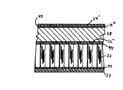
A por~ion of a large size digitizer tablet according to
tne present invention as intended to replace the above-described
tablet of Figure 8 and its method of manufacture is shown in
Figures 11 and 12. A rectangular glass substrate 28 has
conductive ink conductors 12" and 14" applied to respective
opposite surfaces by a silkscreening process and then cured in the
manner taught by the manufacture thereof. Such inks are
commercially available and well known in the art and, therefore,
this aspect of the process will not be described in greater detail
in the interest of simplicity. As depicted in Figure 13, the
conductors 12" and 14" terminate in conductive ink pads 34
adjacent the edges 42 of the glass substrate between which they
extend. A protective sheet of plastic 24' is laminated by means
of an adhesive film 44 to what will be the top surface of the
glass substrate 28. The film 44 is applied directly over the
conductors (12" or 14"). A similar adhesive film 44 (also applied
directly over the other conductors 12" or 14") is employed to
. ~
R
1 3237 07
68567-77
attach the above-described grid components to a honeycomb 26 and
the honeycomb 26 to a backing plate 27. As those skilled in the
art will appreciate, the honeycomb 26 is employed to provide
rigidity to the overall structure and, while preferred because of
its light weight for a given rigidity, it could be replaced by
another material providing the same attributes.
Sd
F~
1 323707
68567-77
The preferred manner of making electrical connectlon to
the conductors 1~' and 14" is shown in Figures 12 and 13. Both
bonding and electrical connection between the pads 34 and matching
conductive pad ends 46 on conductors 48 contalned within a
flexible Mylar connector strip 50 i5 affected by means of a ~o-
called conductive adhesive transfer tape commercially available
from the 3M Company and sold as Scotch brand tape type number 9702
which has certain properties which are particularly adapted to
~olving the requirements of the present invention. The tape 52 is
provided in elongated strips and has an adhesive surface 54 on
both sides. Moreover, the tape 52 has the quality of being
electrically conductive from one side of the tape to the other
through the tape but not longitudinally along the tape.
In working with the tape 52 and the conductive ink, the
applicants herein found that improved performance could be
achieved by employing novel methods devised by the applicants. In
the case of the tape, such improved performance was obtained by
methods completely contrary to the teaching of the manufacturer
of the tape as will be described in greater detail shortly.
The step3 of the preferred overall method for producing
a large ~ize digitizer tablet of low cost-to-manufacture and light
weight are depicted in Figure 17. The flrst step is the
application of a water barrier to the ~urfaces of the glass
substrate 28. This is accomplished by, for example, washing the
glas~ ~ubstrate 28 with a Xcylane wash which cleans the surface of
the glass substrate 28 and leave~ a bonding agent behind on the
~urface which act~ as a water barrier. Without the formation of
the water barrier (l.e., by merely cleaning the surfaces of the
substrate 28 with a commercial glass cleaner or otherwlse), the
conductive ink when applied and cured according to the
manufacturer's specifications ~eemed to adhere adequately; but,
under high amblent humidity conditions, resulted in conductors
12", 14" which could be easily broken by mild scratching. By
employing the water barrier-producing wa~h prlor to applicatlon of
the lnk by silkscreening, the resultant conductors 1~', 14" as
produced are virtually immune to destruction by ~cratching
~ 6
.~
1 323707
6~567-77
regardless of the ambient humidity conditions.
Once the glass of the substrate 28 has been cleaned and
the water barrier formed, the conductors 12'' and conductive pads
34 are applied to one side and cured and then the conductor~ 14"
and conductive pads 34 are applied ~o the other side and cured.
The Mylar connector strips 50 are then applied by first covering
the pads 34 with the tape 52, then rolling the tape 52 into firm
contact with the pads 34 as depicted in Figure 14, and then
pressing the pad ends 46 of the connector strips 50 onto the tape
52 at each pad 34. The rolling procedure was developed by the
applicants herein when it was found that the tape 52 as supplied
by the manufacturer did not work well for lts intended purpose
wlthin the environment of the present invention when merely placed
between components to be fastened (and electrically connected) and
the components pressed
.~. 6a
~;,
1 323707
tnBether. With out the rolling process that was developed to solve the problem, there
was an unacceptably high failure rate at the points of connection.
While it was found that the rolling process improved the bonding of the tape 52
to the pads 34 and the glass of the substrate 28 and that the pad ends 46 and the Mylar
5 of the strips 50 adhered to the rolled tape 52 on the glass substrate 28 to an acceptable
degree, it was found that the tape 52 was virtually useless for bonding pad ends 46 of two
Mylar connector strips 50 together. This is a situation which may occur because of size
of manufacture limitations in the manufacturing of the strips 50; that is, it may be
impossible to make a strip 50 of sufficient length to extend along the entire edge 42 of
o the substrate 28. In the alternative, it may be required or desired to have a connective
strip 50 of L-shape which can extend along to adjoining edges 42 and such an extended
length and shape may be impossible of manufacture. In either case, the strips 50 must
be made in sections and the sections joined by connecting pad ends 46 formed thereon at
overlapping ends using the tape 52. When the tape 52 was placed between the pad ends
46 and the pad ends 46 merely pressed together as recommended by the manufacturer,
the joint failure rate was unacceptable. When the tape 52 was rolled into one pad end
46 and then the other pad end 46 was pressed onto the first pad end 46, the failure rate
was even greater. According to the manufacturer, t vo layers of the tape 52 should never
be employed as the electrical conductive nature of the tape from outer surface to outer
20 surface between the two layers would be destroyed because of the nature and
construction of the tape. After numerous unsuccessful attempts to achieve a satisfactory
adhesive and electrical bond employing the manufacturer's instructions for use, the
applicants herein went contrary to the manufacturer's admonition and employed two
layers of the tape 52 in the manner depicted in Figures 14-16 -- with completely2 5 satisfactory results. Pieces of the tape 52 are rolled into respective ones of the pad ends
46 and adjacent Mylar of the strips 50 to be connected as depicted in Figures 14 and 15.
After rolling to adhere the tape S2 to the strips 50 and pad ends 46, the two pieces of
tape 52 are pressed to~ether as shown in Figure 16. It is surmised by the inventors
herein that the rolling process performs two functions. First, it driYes parting agent on
30 the surface of the tape 52 employed to keep it from sticking to tbe paper tape upon
which it is removably attached for storage, delivery, and application into the body of the
tape 52 adjacent the adhesive outer surface thereof. Second, it causes some realignment
of the conductive particles contained in the tape 52. As a result, the adhesive quality to
other surfaces is diminished; however, the tape 52 is highly adhesiYe to other pieces of
3 s the tape 52. Moreover, because of the realigned nature of the conductive particles, two
1 3237~,
68567-77
rolled layers of the tape 52 are rendered conductive from outer
surface to outer surface, contrary to the expectations of the
manufacturer.
After the connective strips 52 have been attached to the
pads 34 (and to each other as necessary) employing the tape 52 in
the preferred manner described above, the protective sheet of
plastic 24' is laminated to what will be the top surface of the
glass substrate 28 and the above-described grid component~ to a
honeycomb 26 and the honeycomb 26 to a backing plate 27 as
previously mentioned employing an adhesive film 44. The preferred
adhesive film 44 is a *Hylar film having adhesive on both sides
and replaces the resin or other adheslve materlal employed in the
prior art. Thi~ type of adhesive film is well known in the art
for varlous other purposes and is vlrtually welght free ln
addition to being simple and easy to use. Within the lightweight
environment provided by the structure of the present inventlon, it
works well for its intended purpose and adds vlrtually no welght
to the structure itself.
*Trade-mark 8
....